
Related Manuals for Altera Cyclone V SoC


Summary of Contents for Altera Cyclone V SoC
- Page 1 Cyclone V SoC Development Kit User Guide Cyclone V SoC Development Kit User Guide 101 Innovation Drive San Jose, CA 95134 www.altera.com UG-01135-1.0 Feedback Subscribe...
- Page 2 © 2013 Altera Corporation. All rights reserved. ALTERA, ARRIA, CYCLONE, HARDCOPY, MAX, MEGACORE, NIOS, QUARTUS and STRATIX words and logos are trademarks of Altera Corporation and registered in the U.S. Patent and Trademark Office and in other countries. All other words and logos identified as trademarks or service marks are the property of their respective holders as described at www.altera.com/common/legal.html.
-
Page 3: Table Of Contents
Installing the Altera SoC Embedded Development Suite (EDS) ....... . 3–1... - Page 4 How to Contact Altera ........
-
Page 5: Chapter 1. About This Kit
SMB cable. ■ Software The software for this kit, described in the following sections, is available on the Altera website for immediate downloading. You can also request to have Altera mail the software to you on DVDs. Quartus II Web Edition Software The Quartus II Web Edition Software is a licensed set of Altera tools with full functionality. -
Page 6: Cyclone V Soc Development Kit Installer
Cyclone V SoC Development Kit Installer The license-free Cyclone V SoC Development Kit installer includes all the documentation and design examples for the kit. For information on installing the Development Kit Installer, refer to “Installing the... -
Page 7: Chapter 2. Getting Started
“Kit Features” on page 1–1. If any of the items are missing, contact Altera before you proceed. Inspect the Boards To inspect each board, perform these steps: 1. Place the board on an anti-static surface and inspect it to ensure that it has not been damaged during shipment. -
Page 8: References
2–2 Chapter 2: Getting Started References References Use the following links in Table 2–1 to check the Altera website for other related information: Table 2–1. Related Links and Documents Altera Website Link Information Cyclone V SoC Development Kit Latest board design files and reference designs. -
Page 9: Chapter 3. Software Installation
To purchase a subscription, contact your Altera sales representative. Installing the Altera SoC Embedded Development Suite (EDS) The Altera system on a chip (SoC) Embedded Design Suite (EDS) is a comprehensive tool suite for embedded software development on Altera SoC devices. The Altera SoC... -
Page 10: Installing The Development Kit
DVD from the Altera Kit Installations DVD Request Form page of the Altera website. 2. Run the Cyclone V SoC Development Kit installer you acquired in “Software” on page 1–1. 3. Choosing an installation directory that is relative to the Quartus II software installation directory, follow the on-screen instructions to complete the installation process. -
Page 11: Installing The Usb-Blaster Ii Driver
Altera website. On the Altera Programming Cable Driver Information page of the Altera website, locate the table entry for your configuration and click the link to access the instructions. For USB-Blaster II configuration details, refer to the On-Board USB-Blaster II page. - Page 12 3–4 Chapter 3: Software Installation Installing the USB-Blaster II Driver Cyclone V SoC Development Kit May 2013 Altera Corporation User Guide...
-
Page 13: Chapter 4. Development Board Setup
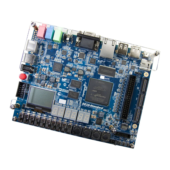
4. Development Board Setup This chapter explains how to set up the Cyclone V SoC development board. Setting Up the Board To prepare the board, perform these steps: 1. The development board ships with its board switches preconfigured to support the design examples in the kit. -
Page 14: Factory Default Switch And Jumper Settings
Factory Default Switch and Jumper Settings This section shows the factory settings (Figure 4–1) for the Cyclone V SoC development board. These settings ensure that the Board Update Portal and Golden System Reference design function properly. The SD card, Max V system controller, and CFI flash are already programmed with the factory default files. - Page 15 ■ OFF (down) = MSEL0 is 1. ■ Switch 2 has the following options: MSEL1 ON (up) = MSEL1 is 0. ■ OFF (down) = MSEL1 is 1. ■ May 2013 Altera Corporation Cyclone V SoC Development Kit User Guide...
- Page 16 ON (up) = Do not include the MAX V system ■ controller in the JTAG chain. OFF (down) = Include the MAX V system controller in ■ the JTAG chain. Cyclone V SoC Development Kit May 2013 Altera Corporation User Guide...
- Page 17 (1) For more information, refer to the Cyclone V Device Handbook. For more information about the FPGA board settings, refer to the Cyclone V SoC Development Board Reference Manual. May 2013 Altera Corporation Cyclone V SoC Development Kit User Guide...
-
Page 18: Restoring The Max V Cpld To The Factory Settings
Configuration is complete when the progress bar reaches 100%. To ensure that you have the most up-to-date factory restore files and product information, refer to the Cyclone V SoC Development Kit page of the Altera website. Cyclone V SoC Development Kit... -
Page 19: Chapter 5. Board Update Portal
5. Board Update Portal The Cyclone V SoC Development Kit ships with the Golden System Reference Design (GSRD) programmed into flash. This design consists of both a hardware and software portion. The hardware portion that is programmed into the FPGA is called the Golden Hardware Reference Design (GHRD) and is programmed into flash device U8. - Page 20 5–2 Chapter 5: Board Update Portal Connecting to the Board Update Portal Web Page Cyclone V SoC Development Kit May 2013 Altera Corporation User Guide...
-
Page 21: Chapter 6. Board Test System
GUI for a board that is in the factory configuration. Look for yellow highlights in the board picture around the corresponding components for each tab. Figure 6–1. Board Test System Graphical User Interface May 2013 Altera Corporation Cyclone V SoC Development Kit User Guide... -
Page 22: Preparing The Board
Navigate to the <install dir>\kits\cycloneVSX_5csxfc6df31es_soc\examples\board_test_system directory and run the BoardTestSystem.exe application. To run the BTS in Windows, you can also click Start > All Programs > Altera > Cyclone V SoC Development Kit <version> > Board Test System. Cyclone V SoC Development Kit... -
Page 23: Using The Board Test System
MAX V ver—Indicates the version of MAX V code currently running on the board. The MAX V code resides in the <install dir>\kits\cycloneVSX_5csxfc6df31es_soc\examples directory. Newer revisions of this code might be available on the Cyclone V SoC Development Kit page of the Altera website. JTAG Chain The JTAG chain control shows all the devices currently in the JTAG chain. -
Page 24: The Gpio Tab
JTAG DIP switch bank (SW4) selects which interfaces are in the chain. Refer to Table 4–3 on page 4–4 for detailed settings. For details on the JTAG chain, refer to the Cyclone V SoC Development Board Reference Manual. For USB-Blaster II configuration details, refer to the On-Board USB-Blaster II page. -
Page 25: Character Lcd
The read-only Push Button switches control displays the current state of the board user push buttons. Press a push button on the board to see the graphical display change accordingly. May 2013 Altera Corporation Cyclone V SoC Development Kit User Guide... -
Page 26: The I2C Tab
■ Range—0x1000 ■ Read—Reads data from the I C EEPROM. For more information on the EEPROM, refer to the Cyclone V SoC Development Board Reference Manual. Real time clock. Cyclone V SoC Development Kit May 2013 Altera Corporation User Guide... -
Page 27: The Ddr3 Tab
DDR3 tab. Figure 6–4. The DDR3 Tab The following sections describe the controls on the DDR3 tab. Start The Start control initiates DDR3 memory transaction performance analysis. May 2013 Altera Corporation Cyclone V SoC Development Kit User Guide... -
Page 28: Stop
The HSMC Tab Refer to “The HSMC Tab” on page 6–12 for the default tab to use for the XCVR, LVDS, and CMOS port loopback tests. Cyclone V SoC Development Kit May 2013 Altera Corporation User Guide... -
Page 29: The Sdi Video Tab
The SDI Video tab allows you to test the SDI video interface on your board. Figure 6–5 shows the SDI Video tab. Figure 6–5. The SDI Video Tab The following sections describe the controls on the SDI Video tab. May 2013 Altera Corporation Cyclone V SoC Development Kit User Guide... -
Page 30: Pattern Generator
Specifies the clock used by the SDI PLL to lock onto. The following choices are available: ■ Lock to host—Locks the SDI PLL to the local reference on the Cyclone V SoC Development board. ■ Lock to input—Locks the SDI PLL to the SDI video data input. - Page 31 ■ PRBS (list)—Selects the transmit pattern and sets the receive error detection circuitry to expect the same pattern for use in loopback testing. May 2013 Altera Corporation Cyclone V SoC Development Kit User Guide...
-
Page 32: The Hsmc Tab
The following sections describe the controls on the HSMC tab. Start, Stop The Start and Stop controls at the bottom-right of this tab allow you to start and stop testing for all three ports. Cyclone V SoC Development Kit May 2013 Altera Corporation User Guide... -
Page 33: Xcrv, Lvds, Cmos
Second post—Specifies the amount of pre-emphasis on the second post tap ■ of the transmitter buffer. Equalizer—Specifies the setting for the receiver equalizer. ■ DC gain—Specifies the DC portion of the receiver equalizer. ■ May 2013 Altera Corporation Cyclone V SoC Development Kit User Guide... -
Page 34: The Power Monitor
<install dir>\kits\cycloneVSX_5csxfc6df31es_soc\examples\board_test_system directory. In Windows, click Start > All Programs > Altera > Cyclone V SoC Development Kit <version> > Power Monitor to start the application. The Power Monitor communicates with the MAX V device on the board through the JTAG bus. -
Page 35: U34 And U26
The Clock Control application runs as a stand-alone application. ClockControl.exe resides in the <install dir>\kits\cycloneVSX_5csxfc6df31es_soc\examples\board_test_system directory. To start the application, click Start > All Programs > Altera > Cyclone V SoC Development Kit <version> > Clock Control. May 2013 Altera Corporation... -
Page 36: Serial Port Registers
The Clock Control For more information about the Si570/Si571 and the Cyclone V development board’s clocking circuitry and clock input pins, refer to the Cyclone V SoC Development Board Reference Manual. The Clock Control communicates with the MAX V device on the board through the JTAG bus. -
Page 37: Default
Target frequency control for the Si570 (X1) and Si571 (X3). Frequency changes might take several milliseconds to take effect. You might see glitches on the clock during this time. Altera recommends resetting the FPGA logic after changing frequencies. - Page 38 6–18 Chapter 6: Board Test System Configuring the FPGA Using the Quartus II Programmer Cyclone V SoC Development Kit May 2013 Altera Corporation User Guide...
-
Page 39: Appendix A. Programming Flash Memory
A. Programming Flash Memory As you develop your own FPGA hardware project using the Altera tools, you can program the flash memory device so that your own design loads from flash memory into the FPGA on power up. This appendix describes the preprogrammed contents of the common flash interface (CFI) flash memory on the development board. -
Page 40: Programming Cfi Flash Using The Quartus Ii Programmer
CFI Flash Memory Programming CFI Flash Using the Quartus II Programmer You can use the JTAG interface in Altera CPLDs to indirectly program the flash memory device. The Altera CPLD JTAG block interfaces directly with the logic array in a special JTAG mode. This mode brings the JTAG chain through the logic array instead of the Altera CPLD boundary-scan cells (BSC). -
Page 41: Converting .Sof Files To A .Pof
MAX CONF DONE LED to turn ON if the writing process is successful. 12. Altera recommends that you return to the Max V System Controller factory design after completing the flash writing. To do so, program the Max V with <install dir>\kits\cycloneVSX_5csxfc6df31es_soc\factory_recovery\max<version>.pof. -
Page 42: Qsfi Flash Memory
11. After the flash writing process has completed, power cycle the board and look for the MAX CONF DONE LED to turn ON if successful. 12. Altera recommends that you return to the Max V System Controller factory design after completing the flash writing. To do so, program the Max V with <install dir>\kits\cycloneVSX_5csxfc6df31es_soc\factory_recovery\max<version>.pof. -
Page 43: Sdi Card Memory
You need to use a disk image program or, preferably, use a Cygwin installation such as the NIOS II Embedded Development System (Nios II EDS). 3. Start the Nios II Command Shell by clicking Start > All Programs > Altera <version> > Nios II EDS > Nios II Command Shell. - Page 44 A–6 Appendix A: Programming Flash Memory SDI Card Memory Cyclone V SoC Development Kit May 2013 Altera Corporation User Guide...
-
Page 45: Additional Information
(software licensing) Email authorization@altera.com Note to Table: (1) You can also contact your local Altera sales office or sales representative. Typographic Conventions The following table shows the typographic conventions this document uses. Visual Cue Meaning Indicate command names, dialog box titles, dialog box options, and other GUI Bold Type with Initial Capital labels. - Page 46 Email Subscription Management Center page of the Altera website, where you can sign up to receive update notifications for Altera documents. The feedback icon allows you to submit feedback to Altera about the document. Methods for collecting feedback vary as appropriate for each document.
Need help?
Do you have a question about the Cyclone V SoC and is the answer not in the manual?
Questions and answers