
Related Manuals for Altera Arria 10 FPGA


Summary of Contents for Altera Arria 10 FPGA
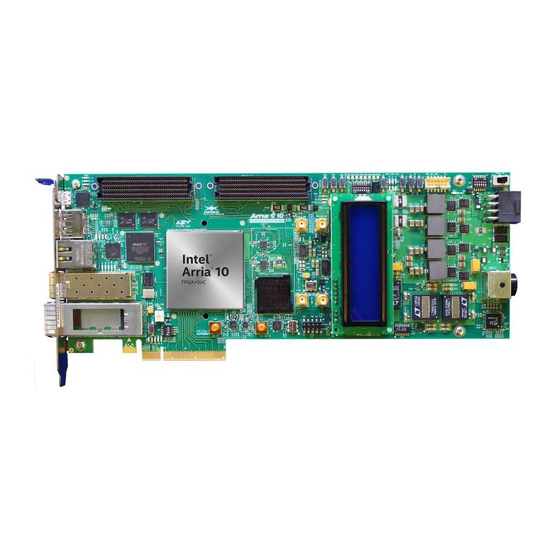
- Page 1 Arria 10 FPGA Development Kit User Guide 101 Innovation Drive UG-01170 Subscribe 2015.06.26 San Jose, CA 95134 Send Feedback www.altera.com...
-
Page 2: Table Of Contents
TOC-2 Arria 10 FPGA Development Kit Contents Overview......................1-1 General Description.............................1-1 Recommended Operating Conditions...................... 1-2 Handling the Board............................. 1-3 Getting Started....................2-1 Installing the Subscription Edition Software................... 2-1 Activating Your License........................2-1 Installing the Development Kit........................2-2 Installing the USB-Blaster Driver......................2-3 Development Board Setup.................. - Page 3 TOC-3 Arria 10 FPGA Development Kit User-Defined Push Buttons......................5-17 User-Defined DIP Switch......................5-17 User-Defined LEDs........................5-18 Character LCD..........................5-18 DisplayPort............................. 5-19 SDI Video Input/Output Ports....................5-20 Clock Circuitry............................5-23 On-Board Oscillators........................5-23 Off-Board Clock I/O........................5-24 Components and Interfaces........................5-25 PCI Express.............................5-25 10/100/1000 Ethernet PHY......................5-28 HiLo External Memory Interface....................
-
Page 4: Overview
Altera assumes no responsibility or liability arising out of the application or use of any information, product, or service described herein except as expressly agreed to in writing by Altera. Altera customers are advised to obtain the latest version of device specifications before relying on any published information and before placing orders for products or services. -
Page 5: Recommended Operating Conditions
UG-01170 Recommended Operating Conditions 2015.06.26 Figure 1-2: Arria 10 GX Block Diagram Micro- MAX II Altera LPC+ Altera LPC+ On-Board USB Blaster & USB Interface JTAG Chain x19 USB Interface HiLO x136 External ENET FPGA Memory (SGMII) Arria 10 GX... -
Page 6: Handling The Board
2015.06.26 Handling the Board When handling the board, it is important to observe static discharge precautions. Caution: Without proper anti-static handling, the board can be damaged. Therefore, use anti-static handling precautions when touching the board. Overview Altera Corporation Send Feedback... -
Page 7: Getting Started
Altera assumes no responsibility or liability arising out of the application or use of any information, product, or service described herein except as expressly agreed to in writing by Altera. Altera customers are advised to obtain the latest version of device specifications before relying on any published information and before placing orders for products or services. -
Page 8: Installing The Development Kit
• Installing the Development Kit 1. Download the Arria 10 FPGA Development Kit installer from the Arria 10 FPGA Development Kit page of the Altera website. Alternatively, you can request a development kit DVD from the Altera Kit Installations DVD Request Form page of the Altera website. -
Page 9: Installing The Usb-Blaster Driver
Installation instructions for the On-Board USB-Blaster II driver for your operating system are available on the Altera website. On the Altera Programming Cable Driver Information page of the Altera website, locate the table entry for your configuration and click the link to access the instructions. -
Page 10: Development Board Setup
Altera assumes no responsibility or liability arising out of the application or use of any information, product, or service described herein except as expressly agreed to in writing by Altera. Altera customers are advised to obtain the latest version of device specifications before relying on any published information and before placing orders for products or services. -
Page 11: Default Switch And Jumper Settings
Do not install or remove jumpers (shunts) while the development board is powered on. Figure 3-1: Default Switch and Jumper Settings on the Top FMCA FMCB PRSNTn 1.35V 1.8V Note for J11 & J 8: 1.5V 1.5V 1.8V 1.35V No shunt = 1.2V FMCB FMCA VCCIO Development Board Setup Altera Corporation Send Feedback... - Page 12 1.35 V FMCB V select CCIO J8 pins 3-4 1.5V 1.5 V FMCB V select CCIO J8 pins 5-6 1.8V 1.8 V FMCB V select CCIO J11 pins 1-2 1.35V 1.35 V FMCA V select CCIO Development Board Setup Altera Corporation Send Feedback...
- Page 13 OFF for SMA input clock selection CLK_EN OFF for setting signal high to the CLK_ENABLE MAV V Si516_FS ON for setting the SDI REFCLK frequency to 148.35 MHz OFF for setting the SDI REFCLK frequency to 148.5 MHz Development Board Setup Altera Corporation Send Feedback...
- Page 14 ON to load user hardware1 from flash OFF to load factory from flash RZQ_B2K ON for setting RZQ resistor of Bank 2K to 99.17 OFF for setting RZQ resistor of Bank 2K to 240 Development Board Setup Altera Corporation Send Feedback...
-
Page 15: Board Test System
Altera assumes no responsibility or liability arising out of the application or use of any information, product, or service described herein except as expressly agreed to in writing by Altera. Altera customers are advised to obtain the latest version of device specifications before relying on any published information and before placing orders for products or services. -
Page 16: Preparing The Board
BoardTestSystem(32-bit).exe or BoardTestSystem(64-bit).exe On Windows, you can also run the BTS from the Start > All Programs > Altera menu. A GUI appears, displaying the application tab that corresponds to the design running in the FPGA. The development board’s flash memory ships preconfigured with the design that corresponds to the GPIO tab. - Page 17 Note: The BTS relies on the Quartus II software's specific library. Before running the BTS, open the Quartus II software. It sets the environment variable automatically. The Board $QUARTUS_ROOTDIR Test System uses this environment variable to locate the Quartus II library. Board Test System Altera Corporation Send Feedback...
-
Page 18: Using The Board Test System
FPGA. The corresponding GUI application tabs that interface with the design are now enabled. If you use the Quartus II Programmer for configuration, rather than the Board Test System GUI, you may need to restart the GUI. Board Test System Altera Corporation Send Feedback... -
Page 19: The System Info Tab
Board Name Indicates the official name of the board, given by the Board Test System. Board P/N Indicates the part number of the board. Serial Number Indicates the serial number of the board. Board Test System Altera Corporation Send Feedback... - Page 20 MAX Ver: Indicates the version of MAX V code currently running on the board. JTAG Chain Shows all the devices currently in the JTAG chain. Qsys Memory Map Shows the memory map of the Qsys system on your board. Board Test System Altera Corporation Send Feedback...
-
Page 21: The Gpio Tab
Displays the current state of the user LEDs for the FPGA. To toggle the board LEDs, click the 0 to 7 buttons to toggle red or green LEDs, or click the All button. Board Test System Altera Corporation Send Feedback... - Page 22 The GPIO Tab 2015.06.26 Push Button Switches Read-only control displays the current state of the board user push buttons. Press a push button on the board to see the graphical display change accordingly. Board Test System Altera Corporation Send Feedback...
-
Page 23: The Flash Tab
Random Test Starts a random data pattern test to flash memory, limited to the 512 K test system scratch page. Board Test System Altera Corporation Send Feedback... - Page 24 Reset Executes the flash device’s reset command and updates the memory table displayed on the Flash tab. Erase Erases flash memory. Flash Memory Map Displays the flash memory map for the development board. Board Test System Altera Corporation Send Feedback...
-
Page 25: The Xcvr Tab
UG-01170 4-11 The XCVR Tab 2015.06.26 The XCVR Tab This tab allows you to perform loopback tests on the QSFP, SFP, SMA, and SDI ports. Figure 4-6: The XCVR Tab Board Test System Altera Corporation Send Feedback... - Page 26 • 2nd post—Specifies the amount of pre-emphasis on the second post tap of the transmitter buffer. Equalizer—Specifies the setting for the receiver equalizer. DC gain—Specifies the DC portion of the receiver equalizer. Board Test System Altera Corporation Send Feedback...
- Page 27 Start—Initiates the selected ports transaction performance analysis. Note: Always click Clear before Start. Stop—Terminates transaction performance analysis. TX and RX performance bars—Show the percentage of maximum theoretical data rate that the requested transactions are able to achieve. Board Test System Altera Corporation Send Feedback...
-
Page 28: The Pcie Tab
This tab allows you to run a PCIe loopback test on your board. You can also load the design and use an oscilloscope to measure an eye diagram of the PCIe transmit signals. Figure 4-7: The PCIe Tab Board Test System Altera Corporation Send Feedback... - Page 29 • 2nd post—Specifies the amount of pre-emphasis on the second post tap of the transmitter buffer. Equalizer—Specifies the setting for the receiver equalizer. DC gain—Specifies the DC portion of the receiver equalizer. Board Test System Altera Corporation Send Feedback...
- Page 30 Start—Initiates the selected ports transaction performance analysis. Note: Always click Clear before Start. Stop—Terminates transaction performance analysis. TX and RX performance bars—Show the percentage of maximum theoretical data rate that the requested transactions are able to achieve. Board Test System Altera Corporation Send Feedback...
-
Page 31: The Fmc A Tab
UG-01170 4-17 The FMC A Tab 2015.06.26 The FMC A Tab This tab allows you to perform loopback tests on the FMC A port. Figure 4-8: The FMC A Tab Board Test System Altera Corporation Send Feedback... - Page 32 • 2nd post—Specifies the amount of pre-emphasis on the second post tap of the transmitter buffer. Equalizer—Specifies the setting for the receiver equalizer. DC gain—Specifies the DC portion of the receiver equalizer. Board Test System Altera Corporation Send Feedback...
- Page 33 Start—Initiates the selected ports transaction performance analysis. Note: Always click Clear before Start. Stop—Terminates transaction performance analysis. TX and RX performance bars—Show the percentage of maximum theoretical data rate that the requested transactions are able to achieve. Board Test System Altera Corporation Send Feedback...
-
Page 34: The Fmc B Tab
UG-01170 4-20 The FMC B Tab 2015.06.26 The FMC B Tab This tab allows you to perform loopback tests on the FMC B port. Figure 4-9: The FMC B Tab Board Test System Altera Corporation Send Feedback... - Page 35 • 2nd post—Specifies the amount of pre-emphasis on the second post tap of the transmitter buffer. Equalizer—Specifies the setting for the receiver equalizer. DC gain—Specifies the DC portion of the receiver equalizer. Board Test System Altera Corporation Send Feedback...
- Page 36 Start—Initiates the selected ports transaction performance analysis. Note: Always click Clear before Start. Stop—Terminates transaction performance analysis. TX and RX performance bars—Show the percentage of maximum theoretical data rate that the requested transactions are able to achieve. Board Test System Altera Corporation Send Feedback...
-
Page 37: The Ddr3 Tab
The DDR3 Tab This tab allows you to read and write DDR3 memory on your board. Figure 4-10: The DDR3 Tab Control Description Start Initiates DDR3 memory transaction performance analysis. Stop Terminates transaction performance analysis. Board Test System Altera Corporation Send Feedback... - Page 38 • Clear—Resets the Detected errors and Inserted errors counters to zeroes. Number of Addresses to Write Determines the number of addresses to use in each iteration of reads and Read and writes. Board Test System Altera Corporation Send Feedback...
-
Page 39: The Ddr4 Tab
The DDR4 Tab This tab allows you to read and write DDR4 memory on your board. Figure 4-11: The DDR4 Tab Control Description Start Initiates DDR4 memory transaction performance analysis. Stop Terminates transaction performance analysis. Board Test System Altera Corporation Send Feedback... - Page 40 • Clear—Resets the Detected errors and Inserted errors counters to zeroes. Number of Addresses to Write Determines the number of addresses to use in each iteration of reads and Read and writes. Board Test System Altera Corporation Send Feedback...
-
Page 41: The Power Monitor
Note: You cannot run the stand-alone power application and the BTS application at the same time. Also, you cannot run power and clock interface at the same time Figure 4-12: Power Monitor Interface Board Test System Altera Corporation Send Feedback... - Page 42 General Information Displays MAX V version and current temperature of the FPGA and board. Reset Clears the graph, resets the minimum and maximum values, and restarts the Power Monitor. Board Test System Altera Corporation Send Feedback...
-
Page 43: The Clock Control
For example, 421.31259873 is possible within 100 parts per million (ppm). The Target frequency control works in conjunction with the Set New Freq control. fXTAL Shows the calculated internal fixed-frequency crystal, based on the serial port register values. Board Test System Altera Corporation Send Feedback... - Page 44 Target frequency control for the programmable oscillators. Frequency changes might take several milliseconds to take effect. You might see glitches on the clock during this time. Altera recommends resetting the FPGA logic after changing frequencies. Each Si5338 tab for U26 and U14 display the same GUI controls for each clock generators. Each tab allows for separate control.
- Page 45 CLK0 to CLK3 controls for the Si5338 (U26 and U14). Frequency changes might take several milliseconds to take effect. You might see glitches on the clock during this time. Altera recommends resetting the FPGA logic after changing frequencies.
- Page 46 UG-01170 4-32 The Clock Control 2015.06.26 Control Description Import Reg Map Import register map file generated from Silicon Laboratories ClockBuilder Desktop. Board Test System Altera Corporation Send Feedback...
-
Page 47: Board Components
Altera assumes no responsibility or liability arising out of the application or use of any information, product, or service described herein except as expressly agreed to in writing by Altera. Altera customers are advised to obtain the latest version of device specifications before relying on any published information and before placing orders for products or services. - Page 48 Controller. Board Reference Type Description Status Elements D22, D23 JTAG LEDs Indicates transmit or receive activity of the JTAG chain. The TX and RX LEDs flicker if the link is in use and active. Board Components Altera Corporation Send Feedback...
- Page 49 125.0-MHz voltage controlled crystal oscillator for the Ethernet interface.. 50-MHz oscillator 50.000-MHz crystal oscillator for general purpose logic. Quad-output oscillator Si5338 programmable oscillator for clock control GUI. (Defaults CLK[0:3] = 270MHz, 644.53125MHz, 644.53125MHz, 133.33MHz) Board Components Altera Corporation Send Feedback...
- Page 50 Communication Ports PCI Express x8 edge Made of gold-plated edge fingers for up to ×8 signaling connector in either Gen1, Gen2, or Gen3 mode. J1, J2 FMC Port FPGA mezzanine card ports A and B. Board Components Altera Corporation Send Feedback...
-
Page 51: Max V Cpld System Controller
PCIe root port. MAX V CPLD System Controller The board utilizes the EPM2210 System Controller, an Altera MAX V CPLD, for the following purposes: • FPGA configuration from flash memory • Power consumption monitoring •... - Page 52 FSM bus flash memory reset FLASH_RESETN 1.8 V FSM bus flash memory write FLASH_WEN 1.8 V enable FM address bus FM_A1 1.8 V FM address bus FM_A2 1.8 V FM address bus FM_A3 1.8 V Board Components Altera Corporation Send Feedback...
- Page 53 FM address bus FM_A22 1.8 V FM address bus FM_A23 1.8 V FM address bus FM_A24 1.8 V FM address bus FM_A25 1.8 V FM address bus FM_A26 1.8 V FM data bus FM_D0 1.8 V Board Components Altera Corporation Send Feedback...
- Page 54 FM data bus FM_D19 1.8 V FM data bus FM_D20 1.8 V FM data bus FM_D21 1.8 V FM data bus FM_D22 1.8 V FM data bus FM_D23 1.8 V FM data bus FM_D24 1.8 V Board Components Altera Corporation Send Feedback...
- Page 55 FPGA configuration data FPGA_CONFIG_ 1.8 V FPGA configuration data FPGA_CONFIG_ 1.8 V FPGA configuration data FPGA_CONFIG_ 1.8 V FPGA configuration data FPGA_CONFIG_ 1.8 V FPGA configuration data FPGA_CONFIG_ 1.8 V FPGA configuration data FPGA_CONFIG_ 1.8 V Board Components Altera Corporation Send Feedback...
- Page 56 FPGA configuration data FPGA_CONFIG_ 1.8 V FPGA configuration data FPGA_CONFIG_ 1.8 V FPGA configuration data FPGA_CONFIG_ 1.8 V FPGA configuration data FPGA_CONFIG_ 1.8 V FPGA configuration data FPGA_CONFIG_ 1.8 V FPGA configuration data FPGA_CONFIG_ 1.8 V Board Components Altera Corporation Send Feedback...
- Page 57 FPGA_NSTATUS 1.8 V FPGA partial reconfiguration FPGA_PR_DONE 1.8 V done FPGA partial reconfiguration FPGA_PR_ERROR K12 1.8 V error FPGA partial reconfiguration FPGA_PR_READY P12 1.8 V ready FPGA partial reconfiguration FPGA_PR_ 1.8 V request REQUEST Board Components Altera Corporation Send Feedback...
- Page 58 MAX V 50 MHz clock MV_CLK_50 1.8 V Temperature monitor fan enable OVERTEMP 2.5 V Temperature monitor fan enable OVERTEMPN 2.5 V Load the flash memory image PGM_CONFIG 2.5 V identified by the PGM LEDs Board Components Altera Corporation Send Feedback...
- Page 59 2.5 V enable MAX1619 device Temperature TSENSE_ALERTN 2.5 V Sense Alert Signal On-board USB-Blaster II USB_CFG0 1.8 V interface (reserved for future use) On-board USB-Blaster II USB_CFG1 1.8 V interface (reserved for future use) Board Components Altera Corporation Send Feedback...
- Page 60 On-board USB-Blaster II USB_CFG13 1.8 V interface (reserved for future use) On-board USB-Blaster II USB_CFG14 1.8 V interface (reserved for future use) On-board USB-Blaster II USB_M5_CLK 1.8 V interface clock ED8101 Alert signal ED8101_ALERT 2.5 V Board Components Altera Corporation Send Feedback...
-
Page 61: Fpga Configuration
The Arria 10 GX FPGA development board includes status LEDs. Table 5-3: Board-Specific LEDs I/O Standard Board Reference Schematic Signal Name MAX_ERROR 2.5 V MAX_LOAD 2.5 V MAX_CONF_DONE 2.5 V FMCA_TX_LED 1.8 V FMCA_RX_LED 1.8 V Board Components Altera Corporation Send Feedback... - Page 62 2.5 V PGM_LED1 2.5 V PGM_LED2 2.5 V FMCA_PRSNTn 1.8 V FMCB_TX_LED 1.8 V FMCB_RX_LED 1.8 V FMCB_PRSNTn 1.8 V PCIE_LED_X1 1.8 V PCIE_LED_X4 1.8 V PCIE_LED_X8 1.8 V PCIE_LED_G2 1.8 V PCIE_LED_G3 1.8 V Board Components Altera Corporation Send Feedback...
-
Page 63: User Input/Output
ON position, a logic 0 is selected. Table 5-5: User-Defined DIP Switch Schematic Signal Names and Functions Board Reference Schematic Signal Name FPGA Pin Number I/O Standard USER_DIPSW0 1.8-V USER_DIPSW1 1.8-V USER_DIPSW2 1.8-V USER_DIPSW3 1.8-V USER_DIPSW4 1.8-V USER_DIPSW5 1.8-V Board Components Altera Corporation Send Feedback... -
Page 64: User-Defined Leds
16 character × 2 line Lumex LCD display. The LCD has a 10-pin receptacle that mounts directly to the board's 10-pin header, so it can be easily removed for access to components under the display. You can also use the header for debugging or other purposes. Board Components Altera Corporation Send Feedback... -
Page 65: Displayport
DP_AUX_CP AN34 LVDS Auxiliary channel (positive) DP_ML_LANE_ AP43 1.4-V PCML Lane 0 (negative) DP_ML_LANE_ AM43 1.4-V PCML Lane 1 (negative) DP_ML_LANE_ AH43 1.4-V PCML Lane 2 (negative) DP_ML_LANE_ AF43 1.4-V PCML Lane 3 (negative) Board Components Altera Corporation Send Feedback... -
Page 66: Sdi Video Input/Output Ports
Table 5-10: SDI Video Output Interface Pin Assignments, Schematic Signal Names, and Functions Board Reference Schematic Signal Name FPGA Pin Number I/O Standard SDI_AVDD — — SDI_AVDD — — SDI_AVDD — — SDI_SD_HDN AW34 1.8 V SDI_TX_RSET — — Board Components Altera Corporation Send Feedback... - Page 67 — — MF0_BYPASS AW32 1.8 V MF1_AUTO_SLEEP AY32 1.8 V MF2_MUTE AY35 1.8 V MF3_XSD — — MODE_SEL — — MUTEREF — — SDI_EQIN_N1 — — SDI_EQIN_P1 — — SDO_N / SDI_RX_N 1.4-V PCML Board Components Altera Corporation Send Feedback...
- Page 68 UG-01170 5-22 SDI Video Input/Output Ports 2015.06.26 Board Reference Schematic Signal Name FPGA Pin Number I/O Standard SDO_P / SDI_RX_P 1.4-V PCML Board Components Altera Corporation Send Feedback...
-
Page 69: Clock Circuitry
B 2A B 2L Buffer PCIE _OB _REFCLK _P /N Si 516 / 133 .33MHz CLK 3 Si 571 644 .53125 MHz CLK 2 Si 5338 644 .53125 MHz CLK 1 270 MHz CLK 0 Board Components Altera Corporation Send Feedback... -
Page 70: Off-Board Clock I/O
MV_CLK_50 Controller clock 50 MHz 1.8 V AU33 Arria 10 FPGA CLK_50 reference clock Off-Board Clock I/O The development board has input and output clocks which can be driven onto the board. The output clocks can be programmed to different levels and I/O standards according to the FPGA device’s specifica‐... -
Page 71: Components And Interfaces
PC's 2x4 ATX auxilary power connected to the 12V ATX input (J4) of the Arria 10 development board. Although the board can also be powered by a laptop power supply for use on a lab bench, Altera recommends that you do not power up from both supplies at the same time. Ideal diode power sharing devices have been designed into this board to prevent damages or back-current from one supply to the other. - Page 72 1.4-V PCML Receive bus PCIE_RX_N5 AK39 1.4-V PCML Receive bus PCIE_RX_N6 AJ41 1.4-V PCML Receive bus PCIE_RX_N7 AH39 1.4-V PCML Receive bus PCIE_RX_P0 AT40 1.4-V PCML Receive bus PCIE_RX_P1 AP40 1.4-V PCML Receive bus Board Components Altera Corporation Send Feedback...
- Page 73 1.4-V PCML Transmit bus PCIE_TX_CP4 AV44 1.4-V PCML Transmit bus PCIE_TX_CP5 AU42 1.4-V PCML Transmit bus PCIE_TX_CP6 AT44 1.4-V PCML Transmit bus PCIE_TX_CP7 AR42 1.4-V PCML Transmit bus PCIE_WAKEN_ AY29 1.8 V Wake signal Board Components Altera Corporation Send Feedback...
-
Page 74: 10/100/1000 Ethernet Phy
The Arria 10 GX FPGA development board supports 10/100/1000 base-T Ethernet using an external Marvell 88E1111 PHY and Altera Triple-Speed Ethernet MegaCore MAC function. The PHY-to-MAC interface employs SGMII using the Arria 10 GX FPGA LVDS pins in Soft-CDR mode at 1.25 Gbps transmit and receive. -
Page 75: Hilo External Memory Interface
• DDR4 x72 (included in the kit) • RLDRAM3 x36 (included in the kit) • QDR IV x36 (not included. Contact your local Altera sales representative for ordering and availability) Table 5-18: HiLo EMI Pin Assignments, Schematic Signal Names Board Reference... - Page 76 MEM_ADDR_CMD16 F33 1.5 V MEM_ADDR_CMD17 G35 1.5 V MEM_ADDR_CMD18 H35 1.5 V MEM_ADDR_CMD19 G33 1.5 V MEM_ADDR_CMD20 U33 1.5 V MEM_ADDR_CMD21 T33 1.5 V MEM_ADDR_CMD22 R34 1.5 V MEM_ADDR_CMD23 P34 1.5 V MEM_ADDR_CMD24 N33 Board Components Altera Corporation Send Feedback...
- Page 77 1.5 V MEM_DMA3 1.5 V MEM_DMB0 AB32 1.5 V MEM_DMB1 AG31 1.5 V MEM_DMB2 1.5 V MEM_DMB3 AC34 1.5 V MEM_DQ_ADDR_ CMD0 1.5 V MEM_DQ_ADDR_ CMD1 1.5 V MEM_DQ_ADDR_ CMD2 1.5 V MEM_DQ_ADDR_ CMD3 Board Components Altera Corporation Send Feedback...
- Page 78 MEM_DQA4 1.5 V MEM_DQA5 1.5 V MEM_DQA6 1.5 V MEM_DQA7 1.5 V MEM_DQA8 1.5 V MEM_DQA9 1.5 V MEM_DQA10 1.5 V MEM_DQA11 1.5 V MEM_DQA12 1.5 V MEM_DQA13 1.5 V MEM_DQA14 1.5 V MEM_DQA15 Board Components Altera Corporation Send Feedback...
- Page 79 1.5 V MEM_DQA30 1.5 V MEM_DQA31 1.5 V MEM_DQA32 1.5 V MEM_DQA33 1.5 V MEM_DQB0 AC31 1.5 V MEM_DQB1 AB31 1.5 V MEM_DQB2 1.5 V MEM_DQB3 1.5 V MEM_DQB4 AD31 1.5 V MEM_DQB5 AD32 Board Components Altera Corporation Send Feedback...
- Page 80 MEM_DQB20 1.5 V MEM_DQB21 1.5 V MEM_DQB22 1.5 V MEM_DQB23 1.5 V MEM_DQB24 AH35 1.5 V MEM_DQB25 AJ34 1.5 V MEM_DQB26 AJ33 1.5 V MEM_DQB27 AH34 1.5 V MEM_DQB28 AD35 1.5 V MEM_DQB29 AE34 Board Components Altera Corporation Send Feedback...
- Page 81 1.5 V MEM_DQSB_N0 AA32 1.5 V MEM_DQSB_N1 AJ31 1.5 V MEM_DQSB_N2 AA33 1.5 V MEM_DQSB_N3 AF34 1.5 V MEM_DQSB_P0 1.5 V MEM_DQSB_P1 AJ32 1.5 V MEM_DQSB_P2 AA34 1.5 V MEM_DQSB_P3 AF33 1.5 V MEM_QKA_P0 Board Components Altera Corporation Send Feedback...
-
Page 82: Fmc
I/O Standard Board Reference Schematic Signal Name FPGA Pin Number FMCA_C2M_PG — FMCA_CLK_M2C_N0 AY19 1.4-V PCML FMCA_CLK_M2C_N1 BA13 1.4-V PCML FMCA_CLK_M2C_P0 AY20 1.4-V PCML FMCA_CLK_M2C_P1 BA12 1.4-V PCML FMCA_DP_C2M_N0 1.4-V PCML FMCA_DP_C2M_N1 1.4-V PCML Board Components Altera Corporation Send Feedback... - Page 83 1.4-V PCML FMCA_DP_C2M_N14 1.4-V PCML FMCA_DP_C2M_N15 1.4-V PCML FMCA_DP_C2M_P0 1.4-V PCML FMCA_DP_C2M_P1 1.4-V PCML FMCA_DP_C2M_P2 1.4-V PCML FMCA_DP_C2M_P3 1.4-V PCML FMCA_DP_C2M_P4 1.4-V PCML FMCA_DP_C2M_P5 1.4-V PCML FMCA_DP_C2M_P6 1.4-V PCML FMCA_DP_C2M_P7 1.4-V PCML FMCA_DP_C2M_P8 1.4-V PCML Board Components Altera Corporation Send Feedback...
- Page 84 1.4-V PCML FMCA_DP_M2C_N5 1.4-V PCML FMCA_DP_M2C_N6 1.4-V PCML FMCA_DP_M2C_N7 1.4-V PCML FMCA_DP_M2C_N8 1.4-V PCML FMCA_DP_M2C_N9 1.4-V PCML FMCA_DP_M2C_N10 1.4-V PCML FMCA_DP_M2C_N11 1.4-V PCML FMCA_DP_M2C_N12 1.4-V PCML FMCA_DP_M2C_N13 1.4-V PCML FMCA_DP_M2C_N14 1.4-V PCML FMCA_DP_M2C_N15 1.4-V PCML Board Components Altera Corporation Send Feedback...
- Page 85 1.4-V PCML FMCA_DP_M2C_P11 1.4-V PCML FMCA_DP_M2C_P12 1.4-V PCML FMCA_DP_M2C_P13 1.4-V PCML FMCA_DP_M2C_P14 1.4-V PCML FMCA_DP_M2C_P15 1.4-V PCML FMCA_GA0 BC16 1.8 V FMCA_GA1 BD16 1.8 V FMCA_GBTCLK_M2C_N0 LVDS FMCA_GBTCLK_M2C_N1 LVDS FMCA_GBTCLK_M2C_P0 LVDS FMCA_GBTCLK_M2C_P1 LVDS FMCA_JTAG_RST — Board Components Altera Corporation Send Feedback...
- Page 86 AT15 LVDS FMCA_LA_RX_N4 AP16 LVDS FMCA_LA_RX_N5 AV18 LVDS FMCA_LA_RX_N6 AU13 LVDS FMCA_LA_RX_N7 AV21 LVDS FMCA_LA_RX_N8 LVDS FMCA_LA_RX_N9 AY12 LVDS FMCA_LA_RX_N10 AY14 LVDS FMCA_LA_RX_N11 AR21 LVDS FMCA_LA_RX_N12 BA14 LVDS FMCA_LA_RX_N13 BB18 LVDS FMCA_LA_RX_N14 AW17 LVDS Board Components Altera Corporation Send Feedback...
- Page 87 AP21 LVDS FMCA_LA_RX_P12 BA15 LVDS FMCA_LA_RX_P13 BB17 LVDS FMCA_LA_RX_P14 AY17 LVDS FMCA_LA_TX_N0 AT22 LVDS FMCA_LA_TX_N1 AP19 LVDS FMCA_LA_TX_N2 AW11 LVDS FMCA_LA_TX_N3 AU17 LVDS FMCA_LA_TX_N4 AV13 LVDS FMCA_LA_TX_N5 AR14 LVDS FMCA_LA_TX_N6 AP17 LVDS FMCA_LA_TX_N7 LVDS Board Components Altera Corporation Send Feedback...
- Page 88 AV11 LVDS FMCA_LA_TX_P3 AT17 LVDS FMCA_LA_TX_P4 AW13 LVDS FMCA_LA_TX_P5 AT14 LVDS FMCA_LA_TX_P6 AR17 LVDS FMCA_LA_TX_P7 LVDS FMCA_LA_TX_P8 AV19 LVDS FMCA_LA_TX_P9 AU11 LVDS FMCA_LA_TX_P10 AY10 LVDS FMCA_LA_TX_P11 AU18 LVDS FMCA_LA_TX_P12 BB15 LVDS FMCA_LA_TX_P13 AT19 LVDS Board Components Altera Corporation Send Feedback...
-
Page 89: Qsfp
I/O Standard Description Name Number QSFP_3P3V_ AL34 1.8 V QSFP interrupt INTERRUPTN QSFP_3P3V_ AK34 1.8 V QSFP low power mode LP_MODE QSFP_3P3V_ AU36 1.8 V Module present MOD_PRSN QSFP_3P3V_ AU35 1.8 V Module select MOD_SELN Board Components Altera Corporation Send Feedback... - Page 90 1.4-V PCML QSFP transmitter data QSFP_TX_N3 1.4-V PCML QSFP transmitter data QSFP_TX_P0 1.4-V PCML QSFP transmitter data QSFP_TX_P1 1.4-V PCML QSFP transmitter data QSFP_TX_P2 1.4-V PCML QSFP transmitter data QSFP_TX_P3 1.4-V PCML QSFP transmitter data Board Components Altera Corporation Send Feedback...
-
Page 91: Sfp
(SDA) and a serial clock (SCL). The MAX V and Arria 10 devices use the I for reading and writing to the character LCD. You can use the Arria 10 or MAX V as the I C host to access the PLLs and clocks. Board Components Altera Corporation Send Feedback... - Page 92 2.5 V C serial clock from MAX V. CLOCK_I2C_SDA 2.5 V C serial data from MAX V. Table 5-23: MAV I C Level Shifter Signals to Arria 10 FPGA Schematic Signal Name Arria 10 Pin Number I/O Standard Description CLOCK_SCL AN30 1.8 V...
- Page 93 LCD Pin Number I/O Standard Description I2C_SCL_DISP 5.0 V LCD I C serial clock from Arria 10 FPGA level shifter. I2C_SDA_DISP 5.0 V LCD I C serial data from Arria 10 FPGA level shifter. Board Components Altera Corporation Send Feedback...
-
Page 94: Memory
Schematic Signal FPGA Pin Name Number FLASH_ADVN BB22 1.8 V Address valid FLASH_CEN1 BB23 1.8 V Chip enable FLASH_CLK BB25 1.8 V Clock FLASH_OEN BC26 1.8 V Output enable FLASH_ AV23 1.8 V Ready RDYBSYN1 Board Components Altera Corporation Send Feedback... - Page 95 1.8 V Address bus FM_A16 AF14 1.8 V Address bus FM_A17 AF15 1.8 V Address bus FM_A18 AH14 1.8 V Address bus FM_A19 AJ12 1.8 V Address bus FM_A20 AJ14 1.8 V Address bus Board Components Altera Corporation Send Feedback...
- Page 96 1.8 V Data bus FM_D27 AR25 1.8 V Data bus FM_D28 AP22 1.8 V Data bus FM_D29 BC19 1.8 V Data bus FM_D30 AU22 1.8 V Data bus FM_D31 BA17 1.8 V Data bus Board Components Altera Corporation Send Feedback...
-
Page 97: Board Power Supply
Power Distribution System The following figure below shows the power distribution system on the A10 FPGA development board. Regulator efficiencies and sharing are reflected in the currents shown, which are at conservative absolute maximum levels. Board Components Altera Corporation Send Feedback... -
Page 98: Power Measurement
MAX V CPLD EPM2210 System Controller as well as the Arria 10 GX FPGA. Daughtercards The Arria 10 development kit provides a full-featured hardware development platform for prototyping and testing high-speed serial interfaces to an Arria 10 GX FPGA. Board Components Altera Corporation Send Feedback... -
Page 99: External Memory Interface
UG-01170 5-53 External Memory Interface 2015.06.26 Table 5-28: Arria 10 FPGA Development Kit Daughtercards Memory Type Transfer Rate (Mbps) Maximum Frequency (MHz) DDR3 2,133 1,066 DDR4 2,666 1,333 RLDRAM 3 2,400 1,200 QDR-IV 2,133 1,066 FMC Loopback Related Information I/O and High Speed I/O Arria 10 Devices... - Page 100 DDR4 SDRAM DDR4 x 72 VDD/2.5 V RLDRAM 3 The RLDRAM 3 x 36 (reduced latency DRAM) controller is designed for use in applications requring high memory throughput, high clock rates and full programmablity. Board Components Altera Corporation Send Feedback...
- Page 101 UG-01170 5-55 QDR-IV 2015.06.26 Figure 5-7: RLDRAM 3 Block Diagram QDR-IV QDR-IV x 36 SRAM devices enable you to maximize memory bandwidth with separate read and write ports. Board Components Altera Corporation Send Feedback...
-
Page 102: Fmc Loopback Card
QVLDB0 QVLDB0 QDRIV_ODT_QVLDB1 QVLDB1 QVLDB1 QDRIV_ODT_DQA0-35 DQA0-35 DQA0-35 QDRIV_ODT_DQB0-35 DQB0-35 DQB0-35 VDD_V1P3 VDDQ (1.2 - 1.8V) V3P3_VTT V3P3 QDRIV_OUT_VREF TPS51200DRC REFOUT VDDQ_V1P2 VLDOIN FMC Loopback Card High Pin Count (HBC) Low Pin Count (LPC) Board Components Altera Corporation Send Feedback... -
Page 103: Additional Information
Altera assumes no responsibility or liability arising out of the application or use of any information, product, or service described herein except as expressly agreed to in writing by Altera. Altera customers are advised to obtain the latest version of device specifications before relying on any published information and before placing orders for products or services.
Need help?
Do you have a question about the Arria 10 FPGA and is the answer not in the manual?
Questions and answers