Table of Contents
Advertisement
Advertisement
Table of Contents

Related Manuals for Altera DE1-SoC


Summary of Contents for Altera DE1-SoC
- Page 1 DE1-SoC User Manual www.terasic.com March 14, 2014 Arrow.com. Downloaded from...
-
Page 2: Table Of Contents
Chapter 3 Using the DE1-SoC Board ............... 12 3.1 Settings of FPGA Configuration Mode ....................12 3.2 Configuration of Cyclone V SoC FPGA on DE1-SoC ................13 3.3 Board Status Elements ..........................19 3.4 Board Reset Elements ..........................19 3.5 Clock Circuitry ............................21 3.6 Peripherals Connected to the FPGA ...................... - Page 3 Chapter 4 DE1-SoC System Builder ................ 53 4.1 Introduction .............................. 53 4.2 Design Flow ............................. 53 4.3 Using DE1-SoC System Builder ......................54 Chapter 5 Examples For FPGA ................60 5.1 DE1-SoC Factory Configuration ......................60 5.2 Audio Recording and Playing ........................61 5.3 Karaoke Machine............................
- Page 4 Chapter 7 Examples for using both HPS SoC and FGPA ........... 99 7.1 HPS Control LED and HEX ........................99 7.2 DE1-SoC Control Panel ......................... 103 Chapter 8 Programming the EPCQ Device .............. 104 8.1 Before The Conversion Begins ....................... 104 8.2 Convert .SOF File to .JIC File ........................
-
Page 5: Chapter 1 De1-Soc Development Kit
Ethernet networking, and much more that promise many exciting applications. The DE1-SoC Development Kit contains all the tools needed to use the board in conjunction with a computer that runs the Microsoft Windows XP or later. -
Page 6: De1-Soc System Cd
USB cable (Type A to Mini-B) for UART control 12V DC power adapter The DE1-SoC System CD contains all the documents and supporting materials associated with DE1-SoC, including the user manual, system builder, reference designs, and device datasheets. -
Page 7: Introduction Of The De1-Soc Board
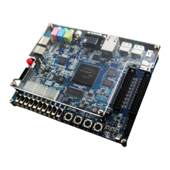
This chapter provides an introduction to the features and design characteristics of the board. Figure 2-1 shows a photograph of the board. It depicts the layout of the board and indicates the location of the connectors and key components. DE1-SoC User Manual www.terasic.com March 14, 2014 Arrow.com. - Page 8 Figure 2-1 DE1-SoC development board (top view) Figure 2-2 De1-SoC development board (bottom view) The DE1-SoC board has many features that allow users to implement a wide range of designed circuits, from simple circuits to various multimedia projects. DE1-SoC User Manual www.terasic.com...
-
Page 9: Block Diagram Of The De1-Soc Board
The following hardware is provided on the board: FPGA Altera Cyclone® V SE 5CSEMA5F31C6N device Altera serial configuration device – EPCQ256 USB-Blaster II onboard for programming; JTAG Mode 64MB SDRAM (16-bit data bus) 4 push-buttons ... - Page 10 Figure 2-3 Block diagram of DE1-SoC Detailed information about Figure 2-3 are listed below. Cyclone V SoC 5CSEMA5F31 Device Dual-core ARM Cortex-A9 (HPS) 85K programmable logic elements 4,450 Kbits embedded memory 6 fractional PLLs 2 hard memory controllers ...
- Page 11 24-bit VGA DAC 24-bit CODEC, Line-in, Line-out, and microphone-in jacks TV decoder (NTSC/PAL/SECAM) and TV-in connector Fast throughput rate: 1 MSPS Channel number: 8 Resolution: 12-bit DE1-SoC User Manual www.terasic.com March 14, 2014 Arrow.com. Arrow.com. Arrow.com.
- Page 12 10 user switches (FPGA x10) 11 user LEDs (FPGA x10, HPS x 1) 2 HPS reset buttons (HPS_RESET_n and HPS_WARM_RST_n) Six 7-segment displays G-Sensor on HPS 12V DC input DE1-SoC User Manual www.terasic.com March 14, 2014 Arrow.com. Arrow.com. Arrow.com.
-
Page 13: Using The De1-Soc Board
This chapter provides an instruction to use the board and describes the peripherals. When the DE1-SoC board is powered on, the FPGA can be configured from EPCQ or HPS. The MSEL[4:0] pins are used to select the configuration scheme. It is implemented as a 6-pin DIP... -
Page 14: Configuration Of Cyclone V Soc Fpga On De1-Soc
SW10.6 Figure 3-1 shows MSEL[4:0] setting of AS mode, which is also the default setting on DE1-SoC. When the board is powered on, the FPGA is configured from EPCQ, which is pre-programmed with the default code. If developers wish to reconfigure FPGA from an application software running on Linux, the MSEL[4:0] needs to be set to “01010”... - Page 15 DE1-SoC board is turned off. When the board is powered on, the configuration data in the EPCQ256 device is automatically loaded into the Cyclone V SoC FPGA. JTAG Chain on DE1-SoC Board The FPGA device can be configured through JTAG interface on DE1-SoC board, but the JTAG chain must form a closed loop, which allows Quartus II programmer to the detect FPGA device.
- Page 16 2. Select detected device associated with the board, as circled in Figure 3-4. Figure 3-4 Select 5CSEMA5 device 3. Both FPGA and HPS are detected, as shown in Figure 3-5. DE1-SoC User Manual www.terasic.com March 14, 2014 Arrow.com. Arrow.com. Arrow.com. Arrow.com.
- Page 17 Figure 3-5 FPGA and HPS detected in Quartus programmer 4. Right click on the FPGA device and open the .sof file to be programmed, as highlighted in Figure 3-6. DE1-SoC User Manual www.terasic.com March 14, 2014 Arrow.com. Arrow.com. Arrow.com. Arrow.com.
- Page 18 Figure 3-7 Select the .sof file to be programmed into the FPGA device 6. Click “Program/Configure” check box and then click “Start” button to download the .sof file into the FPGA device, as shown in Figure 3-8. DE1-SoC User Manual www.terasic.com March 14, 2014 Arrow.com. Arrow.com.
- Page 19 Figure 3-8 Program .sof file into the FPGA device Configure the FPGA in AS Mode The DE1-SoC board uses a quad serial configuration device (EPCQ256) to store configuration data for the Cyclone V SoC FPGA. This configuration data is automatically loaded from the quad serial configuration device chip into the FPGA when the board is powered up.
-
Page 20: Board Status Elements
Illuminate when data is transferred from USB Host to FT232R. UART RXD JTAG_RX Reserved JTAG_TX There are two HPS reset buttons on DE1-SoC, HPS (cold) reset and HPS warm reset, as shown in Figure 3-10. Table 3-4 describes the purpose of these two HPS reset buttons. - Page 21 Figure 3-10 HPS cold reset and warm reset buttons on DE1-SoC Table 3-4 Description of Two HPS Reset Buttons on DE1-SoC Board Reference Signal Name Description Cold reset to the HPS, Ethernet PHY and USB host device. KEY5 HPS_RESET_N Active low input which resets all HPS logics that can be reset.
-
Page 22: Clock Circuitry
Figure 3-11 HPS reset tree on DE1-SoC board Figure 3-12 shows the default frequency of all external clocks to the Cyclone V SoC FPGA. A clock generator is used to distribute clock signals with low jitter. The four 50MHz clock signals connected to the FPGA are used as clock sources for user logic. -
Page 23: Peripherals Connected To The Fpga
Figure 3-12 Block diagram of the clock distribution on DE1-SoC Table 3-5 Pin Assignment of Clock Inputs Signal Name FPGA Pin No. Description I/O Standard CLOCK_50 PIN_AF14 50 MHz clock input 3.3V CLOCK2_50 PIN_AA16 50 MHz clock input 3.3V CLOCK3_50... -
Page 24: User Push-Buttons, Switches And Leds
Figure 3-13 Connections between the push-buttons and the Cyclone V SoC FPGA Pushbutton depressed Pushbutton released Before Debouncing Schmitt Trigger Debounced Figure 3-14 Switch debouncing DE1-SoC User Manual www.terasic.com March 14, 2014 Arrow.com. Arrow.com. Arrow.com. Arrow.com. Arrow.com. Arrow.com. - Page 25 Figure 3-16 shows the connections between LEDs and Cyclone V SoC FPGA. Table 3-6, Table 3-7 Table 3-8 list the pin assignment of user push-buttons, switches, and LEDs. DE1-SoC User Manual www.terasic.com March 14, 2014 Arrow.com. Arrow.com. Arrow.com. Arrow.com. Arrow.com. Arrow.com.
- Page 26 I/O Standard KEY[0] PIN_AA14 Push-button[0] 3.3V KEY[1] PIN_AA15 Push-button[1] 3.3V KEY[2] PIN_W15 Push-button[2] 3.3V KEY[3] PIN_Y16 Push-button[3] 3.3V DE1-SoC User Manual www.terasic.com March 14, 2014 Arrow.com. Arrow.com. Arrow.com. Arrow.com. Arrow.com. Arrow.com. Arrow.com. Arrow.com. Arrow.com. Arrow.com. Arrow.com. Arrow.com. Arrow.com. Arrow.com. Arrow.com.
-
Page 27: 7-Segment Displays
LED [9] 3.3V 3.6.2 7-segment Displays The DE1-SoC board has six 7-segment displays. These displays are paired to display numbers in various sizes. Figure 3-17 shows the connection of seven segments (common anode) to pins on Cyclone V SoC FPGA. The segment can be turned on or off by applying a low logic level or high logic level from the FPGA, respectively. - Page 28 3.3V HEX5[4] PIN_AB26 Seven Segment Digit 5[4] 3.3V HEX5[5] PIN_AA26 Seven Segment Digit 5[5] 3.3V HEX5[6] PIN_AA25 Seven Segment Digit 5[6] 3.3V DE1-SoC User Manual www.terasic.com March 14, 2014 Arrow.com. Arrow.com. Arrow.com. Arrow.com. Arrow.com. Arrow.com. Arrow.com. Arrow.com. Arrow.com. Arrow.com. Arrow.com.
-
Page 29: 2X20 Gpio Expansion Headers
3.3V GPIO_0 [1] PIN_Y17 GPIO Connection 0[1] 3.3V GPIO_0 [2] PIN_AD17 GPIO Connection 0[2] 3.3V GPIO_0 [3] PIN_Y18 GPIO Connection 0[3] 3.3V DE1-SoC User Manual www.terasic.com March 14, 2014 Arrow.com. Arrow.com. Arrow.com. Arrow.com. Arrow.com. Arrow.com. Arrow.com. Arrow.com. Arrow.com. Arrow.com. Arrow.com. - Page 30 GPIO Connection 1[8] 3.3V GPIO_1 [9] PIN_AG25 GPIO Connection 1[9] 3.3V GPIO_1[10] PIN_AG26 GPIO Connection 1[10] 3.3V GPIO_1 [11] PIN_AH24 GPIO Connection 1[11] 3.3V DE1-SoC User Manual www.terasic.com March 14, 2014 Arrow.com. Arrow.com. Arrow.com. Arrow.com. Arrow.com. Arrow.com. Arrow.com. Arrow.com. Arrow.com. Arrow.com. Arrow.com.
-
Page 31: 24-Bit Audio Codec
3.6.4 24-bit Audio CODEC The DE1-SoC board offers high-quality 24-bit audio via the Wolfson WM8731 audio CODEC (Encoder/Decoder). This chip supports microphone-in, line-in, and line-out ports, with adjustable sample rate from 8 kHz to 96 kHz. The WM8731 is controlled via serial I2C bus, which is connected to HPS or Cyclone V SoC FPGA through an I2C multiplexer. -
Page 32: I2C Multiplexer
I2C Data 3.3V 3.6.5 I2C Multiplexer The DE1-SoC board implements an I2C multiplexer for HPS to access the I2C bus originally owned by FPGA. Figure 3-20 shows the connection of I2C multiplexer to the FPGA and HPS. HPS can access Audio CODEC and TV Decoder if and only if the HPS_I2C_CONTROL signal is set to high. -
Page 33: Vga
3.3V 3.6.6 The DE1-SoC board has a 15-pin D-SUB connector populated for VGA output. The VGA synchronization signals are generated directly from the Cyclone V SoC FPGA, and the Analog Devices ADV7123 triple 10-bit high-speed video DAC (only the higher 8-bits are used) transforms signals from digital to analog to represent three fundamental colors (red, green, and blue). - Page 34 More information about the ADV7123 video DAC is available in its datasheet, which can be found on the manufacturer’s website, or in the directory \Datasheets\VIDEO DAC of DE1-SoC System CD. The pin assignment between the Cyclone V SoC FPGA and the ADV7123 is listed in Table 3-16.
- Page 35 640x480 VGA(85Hz) 640x480 SVGA(60Hz) 800x600 SVGA(75Hz) 800x600 SVGA(85Hz) 800x600 XGA(60Hz) 1024x768 XGA(70Hz) 1024x768 XGA(85Hz) 1024x768 1280x1024(60Hz) 1280x1024 1024 DE1-SoC User Manual www.terasic.com March 14, 2014 Arrow.com. Arrow.com. Arrow.com. Arrow.com. Arrow.com. Arrow.com. Arrow.com. Arrow.com. Arrow.com. Arrow.com. Arrow.com. Arrow.com. Arrow.com. Arrow.com. Arrow.com.
-
Page 36: Tv Decoder
3.6.7 TV Decoder The DE1-SoC board is equipped with an Analog Device ADV7180 TV decoder chip. The ADV7180 is an integrated video decoder which automatically detects and converts a standard analog baseband television signals (NTSC, PAL, and SECAM) into 4:2:2 component video data, which is compatible with the 8-bit ITU-R BT.656 interface standard. - Page 37 Table 3-17. More information about the ADV7180 is available on the manufacturer’s website, or in the directory \DE1_SOC_datasheets\Video Decoder of DE1-SoC System CD. Figure 3-23 Connections between the FPGA and TV Decoder Table 3-17 Pin Assignment of TV Decoder Signal Name FPGA Pin No.
-
Page 38: Ir Receiver
The board comes with an infrared remote-control receiver module (model: IRM-V538/TR1), whose datasheet is provided in the directory \Datasheets\ IR Receiver and Emitter of DE1-SoC system CD. The remote controller included in the kit has an encoding chip (uPD6121G) built-in for generating infrared signals. -
Page 39: Sdram Memory
16-bit data line, control line, and address line connected to the FPGA. This chip uses the 3.3V LVCMOS signaling standard. Connections between the FPGA and SDRAM are shown in Figure 3-26, and the pin assignment is listed in Table 3-20. DE1-SoC User Manual www.terasic.com March 14, 2014 Arrow.com. Arrow.com. Arrow.com. - Page 40 DRAM_DQ[2] PIN_AK7 SDRAM Data[2] 3.3V DRAM_DQ[3] PIN_AK8 SDRAM Data[3] 3.3V DRAM_DQ[4] PIN_AK9 SDRAM Data[4] 3.3V DRAM_DQ[5] PIN_AG10 SDRAM Data[5] 3.3V DE1-SoC User Manual www.terasic.com March 14, 2014 Arrow.com. Arrow.com. Arrow.com. Arrow.com. Arrow.com. Arrow.com. Arrow.com. Arrow.com. Arrow.com. Arrow.com. Arrow.com. Arrow.com. Arrow.com.
-
Page 41: Ps/2 Serial Port
SDRAM Chip Select 3.3V 3.6.11 PS/2 Serial Port The DE1-SoC board comes with a standard PS/2 interface and a connector for a PS/2 keyboard or mouse. Figure 3-27 shows the connection of PS/2 circuit to the FPGA. Users can use the PS/2... - Page 42 PIN_AE7 PS/2 Data 3.3V PS2_CLK2 PIN_AD9 PS/2 Clock (reserved for second PS/2 device) 3.3V PS2_DAT2 PIN_AE9 PS/2 Data (reserved for second PS/2 device) 3.3V DE1-SoC User Manual www.terasic.com March 14, 2014 Arrow.com. Arrow.com. Arrow.com. Arrow.com. Arrow.com. Arrow.com. Arrow.com. Arrow.com. Arrow.com.
-
Page 43: A/D Converter And 2X5 Header
3.6.12 A/D Converter and 2x5 Header The DE1-SoC has an analog-to-digital converter (AD7928), which features lower power, eight-channel CMOS 12-bit. This ADC offers conversion throughput rate up to 1MSPS. The analog input range for all input channels can be 0 V to 2.5 V or 0 V to 5V, depending on the RANGE bit in the control register. -
Page 44: Peripherals Connected To Hard Processor System (Hps)
Similar to the FPGA, the HPS also has its set of switches, buttons, LEDs, and other interfaces connected exclusively. Users can control these interfaces to monitor the status of HPS. Table 3-23 gives the pin assignment of all the LEDs, switches, and push-buttons. DE1-SoC User Manual www.terasic.com March 14, 2014 Arrow.com. -
Page 45: Gigabit Ethernet
3-24. More information about the KSZ9021RN PHY chip and its datasheet, as well as the application notes, which are available on the manufacturer’s website. Figure 3-31 Connections between the HPS and Gigabit Ethernet DE1-SoC User Manual www.terasic.com March 14, 2014 Arrow.com. -
Page 46: Uart
HW flow control signals. The physical interface is implemented by UART-USB onboard bridge from a FT232R chip to the host with an USB Mini-B connector. More information about the chip is available on the manufacturer’s website, or in the directory \Datasheets\UART TO DE1-SoC User Manual www.terasic.com March 14, 2014 Arrow.com. -
Page 47: Ddr3 Memory
USB of DE1-SoC system CD. Figure 3-32 shows the connections between the HPS, FT232R chip, and the USB Mini-B connector. Table 3-26 lists the pin assignment of UART interface connected to the HPS. Figure 3-32 Connections between the HPS and FT232R Chip... - Page 48 HPS_DDR3_DQ[20] PIN_P26 HPS DDR3 Data[20] SSTL-15 Class I HPS_DDR3_DQ[21] PIN_P27 HPS DDR3 Data[21] SSTL-15 Class I HPS_DDR3_DQ[22] PIN_N27 HPS DDR3 Data[22] SSTL-15 Class I DE1-SoC User Manual www.terasic.com March 14, 2014 Arrow.com. Arrow.com. Arrow.com. Arrow.com. Arrow.com. Arrow.com. Arrow.com. Arrow.com. Arrow.com.
-
Page 49: Micro Sd Card Socket
1.5 V output drive calibration The board supports Micro SD card interface with x4 data lines. It serves not only an external storage for the HPS, but also an alternative boot option for DE1-SoC board. Figure 3-33 shows signals connected between the HPS and Micro SD card socket. -
Page 50: 2-Port Usb Host
ID pin of USB3300 to ground. When operating in Host mode, the device is powered by the two USB type-A ports. Figure 3-34 shows the connections of USB PTG PHY to the HPS. Table 3-29 lists the pin assignment of USBOTG PHY to the HPS. DE1-SoC User Manual www.terasic.com March 14, 2014 Arrow.com. Arrow.com. Arrow.com. -
Page 51: G-Sensor
I2C interface. The I2C address of G-sensor is 0xA6/0xA7. More information about this chip can be found in its datasheet, which is available on manufacturer’s website or in the directory \Datasheet folder of DE1-SoC system CD. Figure 3-35 shows the connections between the HPS and G-sensor. -
Page 52: Ltc Connector
GPIO, SPI, or I2C based communication with the HPS. Connections between the HPS and LTC connector are shown in Figure 3-36, and the pin assignment of LTC connector is listed in Table 3-31. DE1-SoC User Manual www.terasic.com March 14, 2014 Arrow.com. Arrow.com. Arrow.com. - Page 53 3.3V HPS_SPIM_MISO PIN_E24 SPI Master Input/Slave Output 3.3V HPS_SPIM_MOSI PIN_D22 SPI Master Output /Slave Input 3.3V HPS_SPIM_SS PIN_D24 SPI Slave Select 3.3V DE1-SoC User Manual www.terasic.com March 14, 2014 Arrow.com. Arrow.com. Arrow.com. Arrow.com. Arrow.com. Arrow.com. Arrow.com. Arrow.com. Arrow.com. Arrow.com. Arrow.com.
-
Page 54: De1-Soc System Builder
Chapter 4 DE1-SoC System Builder This chapter describes how users can create a custom design project with the tool named DE1-SoC System Builder. The DE1-SoC System Builder is a Windows-based utility. It is designed to help users create a Quartus II project for DE1-SoC within minutes. The generated Quartus II project files include: ... -
Page 55: Using De1-Soc System Builder
The DE1-SoC System Builder will generate two major files, a top-level design file (.v) and a Quartus II setting file (.qsf) after users launch the DE1-SoC System Builder and create a new project according to their design requirements The top-level design file contains a top-level Verilog HDL wrapper for users to add their own design/logic. - Page 56 The DE1-SoC System Builder is located in the directory: “Tools\SystemBuilder” of the DE1-SoC System CD. Users can copy the entire folder to a host computer without installing the utility. A window will pop up, as shown in Figure 4-2, after executing the DE1-SoC SystemBuilder.exe on the host computer.
- Page 57 4-4. Each component onboard is listed and users can enable or disable one or more components at will. If a component is enabled, the DE1-SoC System Builder will automatically generate its associated pin assignment, including the pin name, pin location, pin direction, and I/O standard.
- Page 58 Figure 4-4 System configuration group GPIO Expansion If users connect any Terasic GPIO-based daughter card to the GPIO connector(s) on DE1-SoC, the DE1-SoC System Builder can generate a project that include the corresponding module, as shown Figure 4-5. It will also generate the associated pin assignment automatically, including pin name, pin location, pin direction, and I/O standard.
- Page 59 The “Prefix Name” is an optional feature that denote the pin name of the daughter card assigned in your design. Users may leave this field blank. Project Setting Management The DE1-SoC System Builder also provides the option to load a setting or save users’ current board configuration in .cfg file, as shown in Figure 4-6.
- Page 60 Figure 4-6 Project Settings Project Generation When users press the Generate button, the DE1-SoC System Builder will generate the corresponding Quartus II files and documents, as listed in Table 4-1: Table 4-1 Files generated by the DE1-SoC System Builder...
-
Page 61: Examples For Fpga
NO space. Otherwise it will lead to error in Nios II. Note Quartus II v13.0 or later is required for all DE1-SoC demonstrations to support Cyclone V SoC device. The DE1-SoC board has a default configuration bit-stream pre-programmed, which demonstrates some of the basic features onboard. -
Page 62: Audio Recording And Playing
Figure 5-1 Command line of the batch file to program the FPGA and EPCQ device This demonstration shows how to implement an audio recorder and player on DE1-SoC board with the built-in audio CODEC chip. It is developed based on Qsys and Eclipse. - Page 63 The audio interface is configured as 16-bit I2S mode. 18.432MHz clock generated by the PLL is connected to the MCLK/XTI pin of the audio chip through the audio controller. DE1-SoC User Manual www.terasic.com March 14, 2014 Arrow.com.
- Page 64 Press KEY2 to start/stop audio playing (note *3) Table 5-1 Slide switches usage for audio source 0 – DOWN Position 1 – UP Position Slide Switches Audio is from MIC-in Audio is from Line-in DE1-SoC User Manual www.terasic.com March 14, 2014 Arrow.com. Arrow.com. Arrow.com. Arrow.com.
-
Page 65: Karaoke Machine
(2). Recording process will stop if the audio buffer is full. (3). Playing process will stop if the audio data is played completely. This demonstration uses the microphone-in, line-in, and line-out ports on DE1-SoC to create a Karaoke machine. The WM8731 CODEC is configured in master mode. The audio CODEC generates AD/DA serial bit clock (BCK) and the left/right channel clock (LRCK) automatically. - Page 66 Users should be able to hear a mixture of microphone sound and the sound from the music player Press KEY0 to adjust the volume; it cycles between volume level 0 to 9 Figure 5-5 illustrates the setup for this demonstration. DE1-SoC User Manual www.terasic.com March 14, 2014 Arrow.com. Arrow.com.
-
Page 67: Sdram Test In Nios Ii
Qsys in this demonstration. It also shows how Altera’s SDRAM controller IP accesses SDRAM and how the Nios II processor reads and writes the SDRAM for hardware verification. The SDRAM controller handles complex aspects of accessing SDRAM such as initializing the memory device, managing SDRAM banks, and keeping the devices refreshed at certain interval. - Page 68 Design Tools Quartus II v13.1 Nios II Eclipse v13.1 Demonstration Source Code Quartus project directory: DE1_SoC_SDRAM_Nios_Test Nios II Eclipse directory: DE1_SoC_SDRAM_Nios_Test \Software DE1-SoC User Manual www.terasic.com March 14, 2014 Arrow.com. Arrow.com. Arrow.com. Arrow.com.
- Page 69 Quartus II v13.1 and Nios II v13.1 must be pre-installed on the host PC. Power on the DE1-SoC board. Connect the DE1-SoC board (J13) to the host PC with a USB cable and install the USB-Blaster driver if necessary.
-
Page 70: Sdram Test In Verilog
Figure 5-7 Display of progress and result for the SDRAM test in Nios II DE1-SoC system CD offers another SDRAM test with its test code written in Verilog HDL. The memory size of the SDRAM bank tested is still 64MB. - Page 71 FPGA configuration file: DE1_SoC_SDRAM_RTL_Test.sof Demonstration Setup Quartus II v13.1 must be pre-installed to the host PC. Connect the DE1-SoC board (J13) to the host PC with a USB cable and install the DE1-SoC User Manual www.terasic.com March 14, 2014 Arrow.com.
-
Page 72: Tv Box Demonstration
ON if the test is PASS after releasing KEY0 LEDR2 Blinks This demonstration turns DE1-SoC board into a TV box by playing video and audio from a DVD player using the VGA output, audio CODEC and the TV decoder on the DE1-SoC board. Figure shows the block diagram of the design. - Page 73 Project directory: DE1_SoC_TV Bitstream used: DE1_SoC_TV.sof Demo batch directory: \DE1_SoC_TV \demo_batch The folder includes the following files: Batch file: DE1_SoC_TV.bat FPGA configuration file : DE1_SoC_TV.sof DE1-SoC User Manual www.terasic.com March 14, 2014 Arrow.com. Arrow.com. Arrow.com. Arrow.com.
- Page 74 Connect the VGA output of the DE1-SoC board to a VGA monitor. Connect the audio output of the DVD player to the line-in port of the DE1-SoC board and connect a speaker to the line-out port. If the audio output jacks from the DVD player are RCA type, an adaptor is needed to convert to the mini-stereo plug supported on the DE1-SoC board.
-
Page 75: Ps/2 Mouse Demonstration
10ms time. The transmit data consists of 12bits, one start bit (as explained before), eight data bits, one parity check bit (odd DE1-SoC User Manual www.terasic.com March 14, 2014 Arrow.com. - Page 76 Figure 5-11 shows the waveform while communication happening on two lines. Figure 5-11 Waveform of clock and data signals during data transmission Project directory: DE1_SoC_PS2_DEMO Bitstream used: DE1_SoC_PS2_DEMO.sof DE1-SoC User Manual www.terasic.com March 14, 2014 Arrow.com. Arrow.com. Arrow.com.
-
Page 77: Ir Emitter Led And Receiver Demonstration
HEX2 Low byte of Y displacement HEX3 High byte of Y displacement DE1-SoC system CD has an example of using the IR Emitter LED and IR receiver. This demonstration is coded in Verilog HDL. DE1-SoC User Manual www.terasic.com March 14, 2014 Arrow.com. - Page 78 “1” and “0”. Logical bits are transmitted as follows: Figure 5-13 Logical '0' – a 562.5µs pulse burst followed by a 562.5µs space with a total transmit time • of 1.125ms DE1-SoC User Manual www.terasic.com March 14, 2014 Arrow.com. Arrow.com.
- Page 79 Note: The signal received by IR Receiver is inverted. For instance, if IR TX Controller sends a lead code 9 ms high and then 4.5 ms low, IR Receiver will receive a 9 ms low and then 4.5 ms high lead code. DE1-SoC User Manual www.terasic.com March 14, 2014 Arrow.com.
- Page 80 The last bit end code represents the end of the frame. The value of this frame is completely inverted at the receiving end. Figure 5-15 Illustration of the remote included in DE1-SoC kit Table 5-5 Key Code Information for Each Key on the Remote...
- Page 81 Shift Register and display on the 7-segment. Figure 5-18 shows the state shift diagram of State Machine block. The input clock should be 50MHz. Figure 5-17 Modules in the IR Receiver controller DE1-SoC User Manual www.terasic.com March 14, 2014 Arrow.com. Arrow.com.
- Page 82 Keep pressing KEY[0] to enable the pattern to be sent out continuously by the IR TX Controller. Observe the six HEXs according to Table 5-6 Release KEY[0] to stop the IR TX. DE1-SoC User Manual www.terasic.com March 14, 2014 Arrow.com. Arrow.com.
-
Page 83: Adc Reading
NIOS II console. Figure 5-19 shows the block diagram of this demonstration. If the input voltage is -2.5V ~ 2.5V, a pre-scale circuit can be used to adjust it to 0 ~ 5V. DE1-SoC User Manual www.terasic.com March 14, 2014 Arrow.com. Arrow.com. - Page 84 Nios II console. Figure 5-20 Pin distribution of the 2x5 Header for the ADC System Requirements The following items are required for this demonstration. DE1-SoC User Manual www.terasic.com March 14, 2014 Arrow.com. Arrow.com.
- Page 85 DE1-SoC board x1 Trimmer Potentiometer x1 Wire Strip x3 Demonstration File Locations Hardware project directory: DE1_SoC_ADC Bitstream used: DE1_SoC_ADC.sof Software project directory: DE1_SoC_ADC software Demo batch file : DE1_SoC_ADC\demo_batch\ DE1_SoC_ADC.bat Demonstration Setup and Instructions ...
-
Page 86: Examples For Hps Soc
Chapter 6 Examples for HPS This chapter provides several C-code examples based on the Altera SoC Linux built by Yocto project. These examples demonstrates major features connected to HPS interface on DE1-SoC board such as users LED/KEY, I2C interfaced G-sensor, and I2C MUX. All the associated files can be found in the directory Demonstrations/SOC of the DE1_SoC System CD. - Page 87 A Makefile is required to compile a project. The Makefile used for this demo is: Compile Please launch Altera SoC EDS Command Shell to compile a project by executing C:\altera\13.1\embedded\Embedded_Command_Shell.bat The "cd" command can change the current directory to where the Hello World project is located.
-
Page 88: Users Led And Key
Execute command: ./my_first_hps Demonstration Setup Connect a USB cable to the USB-to-UART connector (J4) on the DE1-SoC board and the host PC. Copy the demo file "my_first_hps" into a microSD card under the "/home/root" folder in Linux. - Page 89 GPIO Interface. GPIO[28..0] is controlled by the GPIO0 controller and GPIO[57..29] is controlled by the GPIO1 controller. GPIO[70..58] and input-only GPI[13..0] are controlled by the GPIO2 controller. Figure 6-2 Block diagram of GPIO Interface GPIO Register Block DE1-SoC User Manual www.terasic.com March 14, 2014 Arrow.com. Arrow.com. Arrow.com.
- Page 90 The registers of the GPIO1 controller are mapped to the base address 0xFF708000 with 4KB size, and the registers of the GPIO2 controller are mapped to the base address 0xFF70A000 with 4KB size, as shown in Figure 6-3. DE1-SoC User Manual www.terasic.com March 14, 2014 Arrow.com.
- Page 91 alt_clrbits_word: set specified bit value to zero for a specified register The program must include the following header files to use the above API to access the registers of GPIO controller. #include <stdio.h> #include <unistd.h> #include <fcntl.h> DE1-SoC User Manual www.terasic.com March 14, 2014 Arrow.com. Arrow.com. Arrow.com.
- Page 92 HPS_LED is controlled by the bit-24 in the gpio_swporta_dr register of the GPIO1 controller. The status of KEY can be queried by reading the value of the bit-24 in the gpio_ext_porta register of the GPIO1 controller. DE1-SoC User Manual www.terasic.com March 14, 2014 Arrow.com.
- Page 93 ( uint32_t )( HW_REGS_MASK ) ) ), BIT_LED The following statement is used to read the content of gpio_ext_porta register. The bit mask is used to check the status of the key. alt_read_word( ( virtual_base + DE1-SoC User Manual www.terasic.com March 14, 2014 Arrow.com. Arrow.com.
-
Page 94: I2C Interfaced G-Sensor
Execute command: ./hps_gpio Demonstration Setup Connect a USB cable to the USB-to-UART connector (J4) on the DE1-SoC board and the host PC. Copy the executable file "hps_gpio" into the microSD card under the "/home/root" folder in Linux. - Page 95 6-7. The driver name given is '/dev/i2c-0'. Figure 6-7 Connection of HPS I2C signals The step 4 above can be changed to the following to write a value into a register. DE1-SoC User Manual www.terasic.com March 14, 2014 Arrow.com. Arrow.com.
- Page 96 // where szData is an array of six-bytes Demonstration Source Code Build tool: Altera SoC EDS v13.1 Project directory: \Demonstration\SoC\hps_gsensor Binary file: gsensor Build command: make ('make clean' to remove all temporal files) ...
-
Page 97: I2C Mux Test
Figure 6-8 Terminal output of the G-sensor demonstration Press "CTRL + C" to terminate the program. The I2C bus on DE1-SoC is originally accessed by FPGA only. This demonstration shows how to switch the I2C multiplexer for HPS to access the I2C bus. - Page 98 HPS_I2C_CONTROL The following statement is used to set HPS_I2C_CONTROL low. alt_clrbits_word( ( virtual_base + ( ( uint32_t )( ALT_GPIO1_SWPORTA_DR_ADDR ) & ( uint32_t )( HW_REGS_MASK ) ) ), HPS_I2C_CONTROL DE1-SoC User Manual www.terasic.com March 14, 2014 Arrow.com. Arrow.com. Arrow.com. Arrow.com.
- Page 99 Execute command: ./ i2c_switch Demonstration Setup Connect a USB cable to the USB-to-UART connector (J4) on the DE1-SoC board and host PC. Copy the executable file " i2c_switch " into the microSD card under the "/home/root"...
-
Page 100: Chapter 7 Examples For Using Both Hps Soc And Fgpa
Function Block Diagram Figure 7-1 shows the block diagram of this demonstration. The HPS uses Lightweight HPS-to-FPGA AXI Bridge to communicate with FPGA. The hardware in FPGA part is built into DE1-SoC User Manual www.terasic.com March 14, 2014 Arrow.com. Arrow.com. - Page 101 0x01, and the data register offset is 0x00. The following statement is used to retrieve the base address of PIO slave IP. h2p_lw_led_addr=virtual_base+( ( unsigned long )( ALT_LWFPGASLVS_OFST + LED_PIO_BASE ) & ( unsigned long)( HW_REGS_MASK ) ); DE1-SoC User Manual www.terasic.com March 14, 2014 Arrow.com.
- Page 102 Copy the executable files "hps_config_fpga" and "HPS_LED_HEX", and the FPGA configuration file "soc_system_dc.rbf" into the microSD card under the "/home/root" folder in Linux. Insert the booting microSD card into the DE1-SoC board. Please refer to the chapter 5 DE1-SoC User Manual www.terasic.com March 14, 2014 Arrow.com.
- Page 103 Power on the DE1-SoC board. Launch PuTTY to establish connection to the UART port of the DE1-SoC board. Type "root" to login Altera Yocto Linux. Execute "./hps_config_fpga soc_system_dc.rbf " in the UART terminal of PuTTY to configure the FPGA through the FPGA manager.
-
Page 104: De1-Soc Control Panel
DE1-SOC Control Panel. Figure 7-4 Screenshot of DE1-SoC Control Panel Please refer to DE1-SoC_Control_Panel.pdf, which is included in the DE1-SOC System CD for more information on how to build a GUI program step by step. DE1-SoC User Manual www.terasic.com... -
Page 105: Programming The Epcq Device
The FPGA should be set to AS x4 mode i.e. MSEL[4..0] = “10010” to use the quad Flash as a FPGA configuration device. 1. Choose Convert Programming Files from the File menu of Quartus II, as shown in Figure 8-1. DE1-SoC User Manual www.terasic.com March 14, 2014 Arrow.com. Arrow.com. - Page 106 5. Browse to the target directory from the File name field and specify the name of output file. 6. Click on the SOF data in the section of Input files to convert, as shown in Figure 8-2. DE1-SoC User Manual www.terasic.com March 14, 2014 Arrow.com.
- Page 107 8. Select the .sof to be converted to a .jic file from the Open File dialog. 9. Click Open. 10. Click on the Flash Loader and click Add Device, as shown in Figure 8-3. 11. Click OK and the Select Devices page will appear. DE1-SoC User Manual www.terasic.com March 14, 2014 Arrow.com. Arrow.com.
- Page 108 12. Select the targeted FPGA to be programed into the EPCQ, as shown in Figure 8-4. 13. Click OK and the Convert Programming Files page will appear, as shown in Figure 8-5. 14. Click Generate. DE1-SoC User Manual www.terasic.com March 14, 2014 Arrow.com. Arrow.com. Arrow.com. Arrow.com.
- Page 109 Figure 8-4 “Select Devices” page Figure 8-5 “Convert Programming Files” page after selecting the device DE1-SoC User Manual www.terasic.com March 14, 2014 Arrow.com. Arrow.com. Arrow.com. Arrow.com. Arrow.com. Arrow.com. Arrow.com. Arrow.com. Arrow.com. Arrow.com. Arrow.com. Arrow.com. Arrow.com. Arrow.com. Arrow.com. Arrow.com. Arrow.com. Arrow.com.
-
Page 110: Write Jic File Into The Epcq Device
SFL image will be loaded, as shown in Figure 8-7. 6. Click Start to program the EPCQ device. Figure 8-6 Two devices are detected in the Quartus II Programmer DE1-SoC User Manual www.terasic.com March 14, 2014 Arrow.com. Arrow.com. -
Page 111: Erase The Epcq Device
Programming File page will appear. Select the correct .jic file. 5. Erase the EPCQ device by clicking the corresponding Erase box. A factory default SFL image will be loaded, as shown in Figure 8-8. DE1-SoC User Manual www.terasic.com March 14, 2014 Arrow.com. Arrow.com. -
Page 112: Boot From Epcq Device In Quartus Ii V13.1
Figure 8-8 Erase the EPCQ device in Quartus II Programmer 6. Click Start to erase the EPCQ device. There is a known problem in Quartus II software that the Quartus Programmer must be used to program the EPCQ device on DE1-SoC board. Please refer to Altera’s website here with details step by step. -
Page 113: Chapter 9 Appendix
Add Chapter 5 and Chapter 6 V0.3 Modify Chapter 3 V0.4 Add Chapter 3 HPS V0.5 Modify Chapter 3 V1.0 Modify Chapter 8 Copyright © 2014 Terasic Technologies. All rights reserved. DE1-SoC User Manual www.terasic.com March 14, 2014 Arrow.com. Arrow.com. Arrow.com. Arrow.com. Arrow.com. Arrow.com. Arrow.com.
Need help?
Do you have a question about the DE1-SoC and is the answer not in the manual?
Questions and answers