Table of Contents
Advertisement
Quick Links
Download this manual
See also:
Reference Manual
Advertisement
Table of Contents

Related Manuals for Altera Cyclone V GX FPGA


Summary of Contents for Altera Cyclone V GX FPGA
- Page 1 Cyclone V GX FPGA Development Kit User Guide Cyclone V GX FPGA Development Kit User Guide 101 Innovation Drive San Jose, CA 95134 www.altera.com UG-01123-1.1 Feedback Subscribe...
- Page 2 © 2012 Altera Corporation. All rights reserved. ALTERA, ARRIA, CYCLONE, HARDCOPY, MAX, MEGACORE, NIOS, QUARTUS and STRATIX words and logos are trademarks of Altera Corporation and registered in the U.S. Patent and Trademark Office and in other countries. All other words and logos identified as trademarks or service marks are the property of their respective holders as described at www.altera.com/common/legal.html.
-
Page 3: Table Of Contents
Cyclone V GX FPGA Development Kit Installer ........ - Page 4 How to Contact Altera ........
-
Page 5: Chapter 1. About This Kit
Mini SMB cable. ■ Software The software for this kit, described in the following sections, is available on the Altera website for immediate downloading. You can also request to have Altera mail the software to you on DVDs. Quartus II Web Edition Software The Quartus II Web Edition Software is a licensed set of Altera tools with full functionality. -
Page 6: Cyclone V Gx Fpga Development Kit Installer
Cyclone V GX FPGA Development Kit Installer The license-free Cyclone V GX FPGA Development Kit installer includes all the documentation and design examples for the kit. For information on installing the Development Kit Installer, refer to “Installing the... -
Page 7: Chapter 2. Getting Started
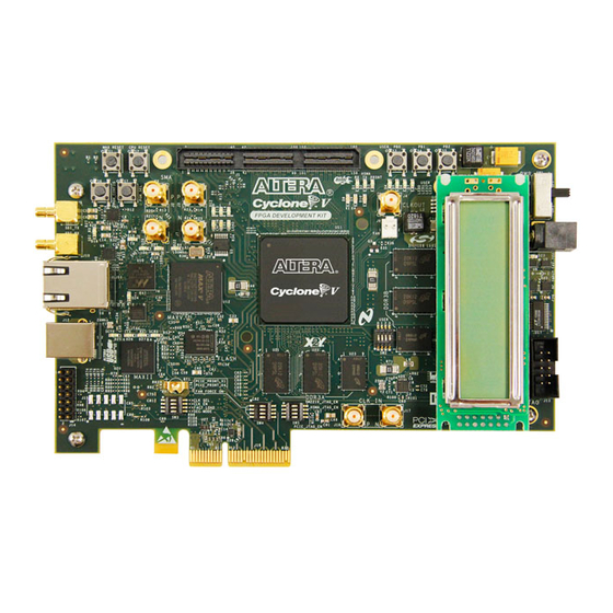
Without proper anti-static handling, you can damage the board. 2. Verify that all components on the boards appear in place and intact. In typical applications with the Cyclone V GX FPGA development board, a heat sink is not necessary. However, under extreme conditions or for engineering sample silicon, the board might require additional cooling to stay within operating temperature guidelines. -
Page 8: References
2–2 Chapter 2: Getting Started References References Use the following links to check the Altera website for other related information: ■ For the latest board design files and reference designs, refer to the Cyclone V GX FPGA Development Kit page. -
Page 9: Chapter 3. Software Installation
Altera Kit Installations DVD Request Form page of the Altera website. 2. Run the Cyclone V GX FPGA Development Kit installer you acquired in “Software” on page 1–1. 3. Choosing an installation directory that is relative to the Quartus II software installation directory, follow the on-screen instructions to complete the installation process. -
Page 10: Installing The Usb-Blaster Ii Driver
Contains the kit documentation. examples Contains the sample design files for the Cyclone V GX FPGA Development Kit. Contains the original data programmed onto the board before shipment. Use this data to restore factory_recovery the board with its original factory contents. -
Page 11: Chapter 4. Development Board Setup
4. Development Board Setup The instructions in this chapter explain how to set up the Cyclone V GX FPGA development board. Setting Up the Board To prepare and apply power to the board, perform these steps: 1. The FPGA development board ships with its board switches preconfigured to support the design examples in the kit. -
Page 12: Factory Default Switch Settings
Off (1) = Programmable oscillator clock is ■ selected. Switch 2 has the following options: CLK EN On (0) = On-board oscillator is disabled. ■ Off (1) = On-board oscillator is enabled. ■ Cyclone V GX FPGA Development Kit October 2012 Altera Corporation User Guide... - Page 13 On (0) = Do not Include the HSMC Port A in the ■ HSMA_JTAG_EN JTAG chain. Off (1) = Include the HSMC Port A in the JTAG ■ chain. October 2012 Altera Corporation Cyclone V GX FPGA Development Kit User Guide...
- Page 14 ■ connector in the JTAG chain. — — — For more information about the FPGA board settings, refer to the Cyclone V GX FPGA Development Board Reference Manual. Cyclone V GX FPGA Development Kit October 2012 Altera Corporation User Guide...
-
Page 15: Chapter 5. Board Update Portal
5. Board Update Portal The Cyclone V GX FPGA Development Kit ships with the Board Update Portal design example stored in the factory portion of the flash memory on the board. The design consists of a Nios II embedded processor, an Ethernet MAC, and an HTML web server. -
Page 16: Using The Board Update Portal To Update User Designs
2. In the Hardware File Name field specify the .flash file that you either downloaded from the Altera website or created on your own. If there is a software component to the design, specify it in the same manner using the Software File Name field;... -
Page 17: Chapter 6. Board Test System
The kit includes a design example and an application called the Board Test System (BTS) to test the functionality of the Cyclone V GX FPGA development board. The BTS provides an easy-to-use interface to alter functional settings and observe the results. -
Page 18: Preparing The Board
4. Set the DIP switch (SW3.3) to the user on (0) position. For more information about the board’s DIP switch and jumper settings, refer to the Cyclone V GX FPGA Development Board Reference Manual. 5. Turn on the power to the board. The board loads the design stored in the user hardware 1 portion of flash memory into the FPGA. -
Page 19: Using The Board Test System
6–3 Using the Board Test System On Windows, click Start > All Programs > Altera > Cyclone V GX FPGA Development Kit <version> > Board Test System to run the application. A GUI appears, displaying the application tab that corresponds to the design running in the FPGA. -
Page 20: Max V Registers
The JTAG chain control shows all the devices currently in the JTAG chain. The Cyclone V GX device is always the first device in the chain. The JTAG chain is normally mastered by the On-board USB-Blaster II. Cyclone V GX FPGA Development Kit October 2012 Altera Corporation User Guide... -
Page 21: Qsys Memory Map
JTAG DIP switch bank (SW5) selects which interfaces are in the chain. Refer to Table 4–3 on page 4–3 for detailed settings. For details on the JTAG chain, refer to the Cyclone V GX FPGA Development Board Reference Manual. For USB-Blaster II configuration details, refer to the On-Board USB-Blaster II page. -
Page 22: Character Lcd
The read-only Push Button switches control displays the current state of the board user push buttons. Press a push button on the board to see the graphical display change accordingly. Cyclone V GX FPGA Development Kit October 2012 Altera Corporation User Guide... -
Page 23: The Flash Tab
Write. The application writes the new values to flash memory and then reads the values back to guarantee that the graphical display accurately reflects the memory contents. October 2012 Altera Corporation Cyclone V GX FPGA Development Kit User Guide... -
Page 24: Random Test
Enter on your keyboard. Then click Write and Read button. Flash Memory Map Displays the flash memory map for the Cyclone V GX FPGA Development Kit. Cyclone V GX FPGA Development Kit October 2012 Altera Corporation... -
Page 25: The Ssram Tab
Write. The application writes the new values to SRAM and then reads the values back to guarantee that the graphical display accurately reflects the memory contents. October 2012 Altera Corporation Cyclone V GX FPGA Development Kit User Guide... -
Page 26: Random Test
<install dir>\kits\cycloneVGX_5cgxfc7df31_fpga\examples\board_test_system directory. On Windows, click Start > All Programs > Altera > Cyclone V GX FPGA Development Kit <version> > Power Monitor to start the application. The Power Monitor communicates with the MAX V device on the board through the JTAG bus. -
Page 27: General Information
■ Update speed—Specifies how often to refresh the graph. Reset This Reset control clears the graph, resets the minimum and maximum values, and restarts the Power Monitor. October 2012 Altera Corporation Cyclone V GX FPGA Development Kit User Guide... -
Page 28: The Clock Control
<install dir>\kits\cycloneVGX_5cgxfc7df31_fpga\examples\board_test_system directory. On Windows, click Start > All Programs > Altera > Cyclone V GX FPGA Development Kit <version> > Clock Control to start the application. For more information about the Si571/Si5388 and the Cyclone V GX FPGA development board’s clocking circuitry and clock input pins, refer to the... -
Page 29: Serial Port Registers
10 and 810 MHz with eight digits of precision to the right of the decimal point. For example, 421.31259873 is possible within 100 parts per million (ppm). The Target frequency control works in conjunction with the Set New Frequency control. October 2012 Altera Corporation Cyclone V GX FPGA Development Kit User Guide... -
Page 30: Read
Target frequency control for the Si571 and the Frequency controls for the Si5338 (U25). Frequency changes might take several milliseconds to take effect. You might see glitches on the clock during this time. Altera recommends resetting the FPGA logic after changing frequencies. -
Page 31: Appendix A. Programming The Flash Memory Device
A. Programming the Flash Memory Device As you develop your own project using the Altera tools, you can program the flash memory device so that your own design loads from flash memory into the FPGA on power up. This appendix describes the preprogrammed contents of the common flash... -
Page 32: Preparing Design Files For Flash Programming
If you have an FPGA design developed using the Quartus II software, and software developed using the Nios II EDS, follow these instructions: 1. On the Windows Start menu, click All Programs > Altera > Nios II EDS > Nios II Command Shell. -
Page 33: Programming Flash Memory Using The Nios Ii Eds
4 User LEDs (D4-D7) illuminate indicating that the flash device is ready for programming. 8. On the Windows Start menu, click All Programs > Altera > Nios II EDS > Nios II Command Shell. 9. In the Nios II command shell, navigate to the <install dir>\kits\cycloneVGX_5cgxfc7df31_fpga\factory_recovery directory (or to the... -
Page 34: Restoring The Flash Device To The Factory Settings
4 User LEDs (D4-D7) illuminate indicating that the flash device is ready for programming. The flash device is ready for programming. 6. On the Windows Start menu, click All Programs > Altera > Nios II EDS > Nios II Command Shell. 7. In the Nios II command shell, navigate to the <install dir>\kits\cycloneVGX_5cgxfc7df31_fpga\factory_recovery directory and type... -
Page 35: Restoring The Max V Cpld To The Factory Settings
To ensure that you have the most up-to-date factory restore files and information about this product, refer to the Cyclone V GX FPGA Development Kit page of the Altera website. Restoring the MAX V CPLD to the Factory Settings This section describes how to restore the original factory contents to the MAX V CPLD on the FPGA development board. - Page 36 A–6 Appendix A: Programming the Flash Memory Device Restoring the MAX V CPLD to the Factory Settings Cyclone V GX FPGA Development Kit October 2012 Altera Corporation User Guide...
-
Page 37: Additional Information
(software licensing) Email authorization@altera.com Note to Table: (1) You can also contact your local Altera sales office or sales representative. Typographic Conventions The following table shows the typographic conventions this document uses. Visual Cue Meaning Indicate command names, dialog box titles, dialog box options, and other GUI Bold Type with Initial Capital labels. - Page 38 Email Subscription Management Center page of the Altera website, where you can sign up to receive update notifications for Altera documents. The feedback icon allows you to submit feedback to Altera about the document. Methods for collecting feedback vary as appropriate for each document.
Need help?
Do you have a question about the Cyclone V GX FPGA and is the answer not in the manual?
Questions and answers