Table of Contents
Advertisement
Quick Links
UM1855
User manual
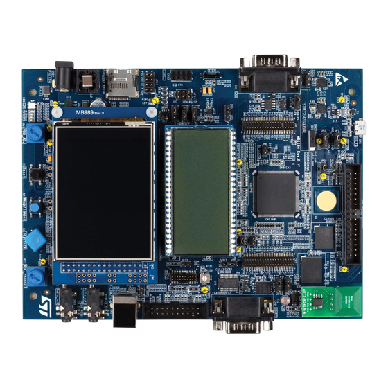
Evaluation board with STM32L476ZGT6 MCU
Introduction
The STM32L476G-EVAL evaluation board is designed as complete demonstration and
development platform for STMicroelectronics ARM
®
Cortex
®
-M4-core-based
STM32L476ZGT6 microcontroller with three I²C buses, three SPI and six USART ports,
CAN port, SWPMI, two SAI ports, 12-bit ADC, 12-bit DAC, LCD driver, internal 128-Kbyte
SRAM and 1-Mbyte Flash memory, Quad-SPI port, touch sensing capability, USB OTG FS
port, LCD controller, flexible memory controller (FMC), JTAG debug port.
(1)
STM32L476G-EVAL, shown in
Figure 1
, can be used as reference design for user
application development, although it is not considered as final application.
A full range of hardware features on the board helps users evaluate all on-board peripherals
such as USB, USART, digital microphones, ADC and DAC, dot-matrix TFT LCD, LCD glass
module, IrDA, LDR, SRAM, NOR Flash memory device, Quad-SPI Flash memory device,
microSD card, sigma-delta modulators, smartcard with SWP, CAN transceiver, EEPROM,
RF-EEPROM. Extension headers allow connecting daughterboards or wrapping boards.
ST-LINK/V2-1 in-circuit debugger and flashing facility is integrated on the mainboard.
Figure 1. STM32L476G-EVAL evaluation board
1. Picture not contractual.
September 2015
DocID027351 Rev 3
1/100
www.st.com
1
Advertisement
Table of Contents

Subscribe to Our Youtube Channel
Related Manuals for STMicroelectronics STM32L476G-EVAL


Summary of Contents for STMicroelectronics STM32L476G-EVAL
-
Page 1: Figure 1. Stm32L476G-Eval Evaluation Board
UM1855 User manual Evaluation board with STM32L476ZGT6 MCU Introduction The STM32L476G-EVAL evaluation board is designed as complete demonstration and development platform for STMicroelectronics ARM ® Cortex ® -M4-core-based STM32L476ZGT6 microcontroller with three I²C buses, three SPI and six USART ports,... -
Page 2: Table Of Contents
STM32L476G-EVAL used as USB device ..... . . 23 2.8.2 STM32L476G-EVAL used as USB host ......24 2.8.3 Configuration elements related with USB OTG FS port . - Page 3 UM1855 Contents 2.9.4 Operating voltage ......... 26 2.10 LPUART port .
- Page 4 Contents UM1855 2.26.1 Limitations ..........48 2.27 Smartcard, SWP .
- Page 5 UM1855 Contents Appendix B Federal Communications Commission (FCC) and Industry Canada (IC) Compliance Statements ... . 98 FCC Compliance Statement ........98 B.1.1 Part 15.19 .
- Page 6 List of tables UM1855 List of tables Table 1. Setting of configuration elements for trace connector CN12 ..... . . 14 Table 2.
- Page 7 STM32L476G-EVAL main component layout ........12...
- Page 8 List of figures UM1855 Figure 49. USB_OTG_FS port schematic diagram ........90 Figure 50.
-
Page 9: Overview
UM1855 Overview Overview Features • STM32L476ZGT6 microcontroller with 1-Mbyte Flash memory and 128-Kbyte RAM • four power supply options: power jack, ST-LINK/V2-1 USB connector, USB OTG FS connector, daughterboard • microcontroller supply voltage: 3.3 V or range from 1.71 V to 3.6 V •... -
Page 10: Demonstration Software
Demonstration software is preloaded in the STM32L476ZGT6 Flash memory, for easy demonstration of the device peripherals in stand-alone mode. For more information and to download the latest available version, refer to the STM32L476G-EVAL demonstration software available on www.st.com. Order code To order the evaluation board based on the STM32L476ZGT6 MCU, use the order code STM32L476G-EVAL. -
Page 11: Hardware Layout And Configuration
UM1855 Hardware layout and configuration Hardware layout and configuration The STM32L476G-EVAL evaluation board is designed around STM32L476ZGT6 target microcontroller in LQFP 144-pin package. Figure 2 illustrates STM32L476ZGT6 connections with peripheral components. Figure 3 shows the location of main components on the evaluation board. -
Page 12: Figure 3. Stm32L476G-Eval Main Component Layout
Hardware layout and configuration UM1855 Figure 3. STM32L476G-EVAL main component layout 12/100 DocID027351 Rev 3... -
Page 13: St-Link/V2-1
2.1.1 Drivers Before connecting STM32L476G-EVAL to a Windows 7, Windows 8 or Windows XP PC via USB, a driver for ST-LINK/V2-1 must be installed. It can be downloaded from www.st.com. In case the STM32L476G-EVAL evaluation board is connected to the PC before installing the driver, the Windows device manager may report some USB devices found on STM32L476G-EVAL as “Unknown”. -
Page 14: St-Link/V2-1 Firmware Upgrade
For its own operation, ST-LINK/V2-1 employs a dedicated MCU with Flash memory. Its firmware determines ST-LINK/V2-1 functionality and performance. The firmware may evolve during the life span of STM32L476G-EVAL to include new functionality, fix bugs or support new target microcontroller families. It is therefore recommended to keep ST-LINK/V2-1 firmware up to date. -
Page 15: Power Supply
2.3.1 Supplying the board through ST-LINK/V2-1 USB port To power STM32L476G-EVAL in this way, the USB host (a PC) gets connected with the STM32L476G-EVAL board’s Standard-B USB receptacle, via a USB cable. This event starts the USB enumeration procedure. In its initial phase, the host’s USB port current supply capability is limited to 100 mA. -
Page 16: Using St-Link/2-1 Along With Powering Through Cn22 Power Jack
The host PC is capable of supplying 300 mA (the enumeration succeeds) and it has a built-in over-current protection on its USB port, limiting or shutting down the power out of its USB port when the excessive current demand from STM32L476G-EVAL is detected. This causes an operating failure to STM32L476G-EVAL. -
Page 17: Table 2. Power-Supply-Related Jumper Settings
Jumper setting Configuration JP17 STM32L476G-EVAL is supplied through CN22 power jack (marked PSU_E5V). CN6 extension connector does not pass the 5 V of STM32L476G-EVAL to daughterboard. JP17 STM32L476G-EVAL is supplied through CN1 Micro-AB USB connector. CN6 extension connector does not pass the 5 V of STM32L476G-EVAL to daughterboard. - Page 18 VDD_IO connection VDD_IO is open. Default setting. JP18 Standard-B USB connector CN17 of ST-LINK/V2-1 can supply power to the STM32L476G-EVAL board JP18 remainder, depending on host PC USB port’s powering capability declared in the enumeration. Powering through USB of Standard-B USB connector CN17 of ST-LINK/V2-1...
-
Page 19: Clock References
UM1855 Hardware layout and configuration Clock references Two clock references are available on STM32L476G-EVAL for the STM32L476ZGT6 target microcontroller: • 32.768 kHz crystal X1, for embedded RTC • 8 MHz crystal X2, for main clock generator The main clock can also be generated using an internal RC oscillator. The X2 crystal is in a socket. -
Page 20: Boot
Hardware layout and configuration UM1855 Sources of reset are: • reset button B1 • JTAG/SWD connector CN15 and ETM trace connector CN12 (reset from debug tools) • through extension connector CN7, pin 32 (reset from daughterboard) • ST-LINK/V2-1 • RS-232 connector CN9, terminal 8 (CTS signal), if JP9 is closed (open by default) Boot 2.6.1 Boot options... -
Page 21: Bootloader Limitations
USART, SPI, I²C bus, USB or CAN. Bootloader version can be identified by reading Bootloader ID at the address 0x1FFF6FFE. The STM32L476ZGT6 part soldered on the STM32L476G-EVAL main board is marked with a date code corresponding to its date of manufacture. STM32L476ZGT6 parts with the date code prior or equal to week 22 of 2015 are fitted with bootloader V 9.0 affected by the... -
Page 22: Digital Microphones
2.7.1 Digital microphones U35 and U36 on board of STM32L476G-EVAL are MP34DT01TR MEMS digital omni- directional microphones providing PDM (pulse density modulation) outputs. To share the same data line, their outputs are interlaced. The combined data output of the microphones is directly routed to STM32L476ZGT6 terminals, thanks to the integrated input digital filters. -
Page 23: Limitations In Using Audio Features
The JP19 jumper must be left open to prevent STM32L476G-EVAL from sourcing 5 V to VBUS terminal, which would cause conflict with the 5 V sourced by the USB host. This may... -
Page 24: Stm32L476G-Eval Used As Usb Host
When a “USB device” connection to the CN1 Micro-AB USB connector is detected, the STM32L476G-EVAL board starts behaving as “USB host”. It sources 5 V on the VBUS terminal of CN1 Micro-AB USB connector to power the USB device. For this to happen, the STM32L476ZGT6 MCU sets the U1 power switch STMPS2151STR to ON state. -
Page 25: Limitations In Using Usb Otg Fs Port
The USB-related operating supply voltage of STM32L476ZGT6 (VDD_USB line) must be within the range from 3.0 V to 3.6 V. RS-232 and IrDA ports The STM32L476G-EVAL board offers one RS-232 communication port and one IrDA port. 2.9.1 RS-232 port The RS-232 communication port uses the DE-9M 9-pole connector CN9. RX, TX, RTS and CTS signals of USART1 port of STM32L476ZGT6 are routed to CN9. -
Page 26: Irda Port
Hardware layout and configuration UM1855 For configuration elements related with the RS-232 port operation, refer to Table 6 Table Section 2.10 brings information on using the LPUART port of STM32L476ZGT6 for RS-232, instead of its USART1 port. 2.9.2 IrDA port The IrDA communication port uses an IrDA transceiver (U11). -
Page 27: Microsd Card
UM1855 Hardware layout and configuration In the default configuration of STM32L476G-EVAL, the RX and TX terminals of the LPUART port are routed to the USB virtual COM port of ST-LINK/V2-1 and, the RX and TX terminals of USART1 port to the RS-232 connector CN9. -
Page 28: Motor Control
Hardware layout and configuration UM1855 2.12 Motor control The CN2 connector is designed to receive a motor control (MC) module. Table 12 shows the assignment of CN2 and STM32L476ZGT6 terminals. Table 12 also lists the modifications to be made on the board versus its by-default configuration. -
Page 29: Board Modifications To Enable Motor Control
UM1855 Hardware layout and configuration Table 12. Motor control terminal and function assignment (continued) Motor control STM32L476ZGT6 microcontroller connector CN2 Terminal Alternate Board modifications for Terminal Port name Function name function enabling motor control PhaseB current- PhaseC Close SB42 ADC123_IN current+ Remove MB979 daughterboard PhaseC... -
Page 30: Figure 7. Pcb Top-Side Rework For Motor Control
Hardware layout and configuration UM1855 Figure 7. PCB top-side rework for motor control 30/100 DocID027351 Rev 3... -
Page 31: Limitations
2.13 The STM32L476G-EVAL board supports one CAN2.0A/B channel compliant with CAN specification. The CN5 9-pole male connector of DE-9M type is available as CAN interface. A 3.3 V CAN transceiver is fitted between the CN5 connector and the CAN controller port of STM32L476ZGT6. -
Page 32: Limitations
Limitations CAN operation is exclusive with LCD glass module operation. 2.13.2 Operating voltage The supply voltage for STM32L476G-EVAL CAN operation must be within the range from 3.0 V to 3.6 V. 2.14 Extension connectors CN6 and CN7 The CN6 and CN7 headers complement the LCD glass module daughterboard connector, to give access to all GPIOs of the STM32L476ZGT6 microcontroller. -
Page 33: Figure 9. Lcd Glass Module Daughterboard In Display Position
UM1855 Hardware layout and configuration connectors on the daughterboard have three rows of holes each. One raw is routed to segments of the LCD. The other two rows are interconnected and form a series of jumpers. The way of inserting the LCD glass module daughterboard into CN11 and CN14 headers determines two functions of LCD glass module daughterboard. -
Page 34: Table 14. Lcd-Daughterboard-Related Configuration Elements
Hardware layout and configuration UM1855 Figure 10. LCD glass module daughterboard in I/O-bridge position Table 14. LCD-daughterboard-related configuration elements Setting to enable Element LCD glass Description segment module PA1 routed to LCDSEG0 SEG0 SB32 Open PA1 not routed to motor control PA2 routed to LCDSEG1 SEG1 SB31... - Page 35 UM1855 Hardware layout and configuration Table 14. LCD-daughterboard-related configuration elements (continued) Setting to enable Element LCD glass Description segment module PB11 routed to LCDSEG11 SEG11 Open PB11 not routed to Quad-SPI Flash memory device PB12 routed to LCDSEG12 SEG12 Open PB12 not routed to Quad-SPI Flash memory device PB13 routed to LCDSEG13 SEG13...
-
Page 36: Table 15. Lcd Glass Element Mapping - Segments 0 To 9
Hardware layout and configuration UM1855 corresponding to each COMx and SEGy combination. Names in quoting marks denote elements forming textual symbols, for example “µA” or “+”. Figure 11 shows the physical location and shape of each segment on the LCD glass module. Table 15. -
Page 37: Limitations
UM1855 Hardware layout and configuration Table 18. LCD glass element mapping - segments 30 to 39 SEG30 SEG31 SEG32 SEG33 SEG34 SEG35 SEG36 SEG37 SEG38 SEG39 COM0 COM1 COM2 COM3 COM4 COM5 COM6 COM7 2.15.1 Limitations LCD glass module operation is exclusive with all other features of the board. DocID027351 Rev 3 37/100... -
Page 38: Figure 11. Lcd Glass Display Element Mapping
Figure 11. LCD glass display element mapping... -
Page 39: Tft Lcd Panel
UM1855 Hardware layout and configuration 2.16 TFT LCD panel STM32L476G-EVAL is delivered with MB989P, a daughterboard plugged into the CN19 extension connector. It bears a TFT 2.8-inch color LCD panel with resistive touchscreen and an on-board controller. Section 2.18 provides further information. -
Page 40: User Leds
LED3 (Red) STM32L476ZGT6 LED4 (Blue) GPIO2 IOExpander1 2.18 Physical input devices The STM32L476G-EVAL board provides a number of input devices for physical human control. These are: • four-way joystick controller with select key (B3) • wake-up/ tamper button (B2) •... -
Page 41: Limitations
Operational amplifier STM32L476ZGT6 provides two on-board operational amplifiers, one of which, OpAmp1, is made accessible on STM32L476G-EVAL. OpAmp1 has its inputs and its output routed to I/O ports PA0, PA1 and PA3, respectively. The non-inverting input PA0 is accessible on the terminal 1 of the JP7 jumper header. -
Page 42: Comparator
STM32L476ZGT6 provides two on-board comparators, one of which, Comp2, is made accessible on STM32L476G-EVAL. Comp2 has its non-inverting input and its output routed to I/O ports PB4 and PB5, respectively. The input is accessible on the terminal 3 of the JP7 jumper header. -
Page 43: Limitations
By default, the FMC_NWAIT signal is not routed to RB port of the NOR Flash memory device, and, to know its ready status, its status register is polled by the demo software fitted in STM32L476G-EVAL. This can be modified with configuration elements, as shown in Table... -
Page 44: Limitations
EEPROM M24128-DFDW6TP, a 128-Kbit I²C-bus EEPROM device, is fitted on the main board of STM32L476G-EVAL, in U6 position. it is accessed with I²C-bus lines I2C2_SCL and I2C2_SDA of STM32L476ZGT6. It supports all I²C-bus modes with speeds up to 1 MHz. -
Page 45: Quad-Spi Flash Memory Device
Quad-SPI Flash memory device N25Q256A13EF840E, a 256-Mbit Quad-SPI Flash memory device, is fitted on the STM32L476G-EVAL main board, in U9 position. It allows evaluating STM32L476ZGT6 Quad-SPI Flash memory device interface. N25Q256A13EF840E can operate in single transfer rate (STR) and double transfer rate (DTR) modes. -
Page 46: Limitations
2.26 Touch-sensing button The STM32L476G-EVAL evaluation board supports a touch sensing button based on either RC charging or on charge-transfer technique. The latter is enabled, by default. The touch sensing button is connected to PB12 port of STM32L476ZGT6 and the related charge capacitor is connected to PB13. -
Page 47: Table 27. Touch-Sensing-Related Configuration Elements
UM1855 Hardware layout and configuration Table 27. Touch-sensing-related configuration elements Element Setting Configuration Default setting. PB12 port is routed to CN11 connector for LCD glass module daughterboard. This setting is not good for robustness of touch sensing. PB12 port is cut from CN11. This setting is good for robustness of touch sensing. -
Page 48: Limitations
Smartcard, SWP ST8024CDR, an interface device for 3 V and 5 V asynchronous smartcards, is fitted on the STM32L476G-EVAL main board, in U30 position. ST8024CDR performs all supply protection and control functions of the smartcard. ST8024CDR is controlled, on its turn, by STM32L476ZGT6, directly through its ports or... -
Page 49: Table 29. Configuration Elements Related With Smartcard And Swp
UM1855 Hardware layout and configuration Table 29. Configuration elements related with smartcard and SWP Element Setting Configuration Default setting. R109 in Smartcard SWP cannot be handled: R39 in PB12 is routed to USB OTG FS port as USBOTG_OVRCR line, on SB3 open top of being routed to SWIO port of smartcard CN11 I/O-bridged... -
Page 50: Limitations
= 3.6 V. However, the SWP only operates with the supply voltage of 3.3 V. 2.28 Near-field communication (NFC) The STM32L476G-EVAL board can host an NFC transceiver board plugged in CN13 extension connector. Figure 12 illustrates the way of attaching an NFC board. -
Page 51: Dual-Channel Sigma-Delta Modulators Stpms2L
DFSDM_CKOUT clock generated by the STM32L476ZGT6 DFSDM controller and received on CLK terminal of STPMS2L. There are two STPMS2L devices on STM32L476G-EVAL, sharing the DFSDM clock. One is wired such as to support a power-metering demonstrator. The other allows measuring temperature using the PT100 sensor. -
Page 52: Stpms2L Settings
Figure 13. Routing of STPMS2L dual-channel sigma-delta modulators 2.29.2 STPMS2L settings STPMS2L operating parameters are set through its configuration terminals MS0, MS1, MS2 and MS3. On STM32L476G-EVAL, both devices are configured as follows: • voltage channel range: differential voltage +/- 300mV •... -
Page 53: Figure 14. Power Measurement Principle Schematic Diagram
UM1855 Hardware layout and configuration Figure 14. Power measurement principle schematic diagram A low-voltage AC generator is to be applied by the user as shown in Figure 14. The shunt resistor is connected in series with the load to provide current measurement points to one of STPMS2L input channels. -
Page 54: Stpms2L For Pt100 Measurement
(IDD) in Run and Low-power modes, except for Shutdown mode. It is strongly recommended that, the MCU supply voltage (VDD_MCU line) does not exceed 3.3 V. This is because there are components on STM32L476G-EVAL supplied from 3.3 V 54/100 DocID027351 Rev 3... -
Page 55: Idd Measurement Principle - Analog Part
UM1855 Hardware layout and configuration that communicate with the MCU through I/O ports. Voltage exceeding 3.3 V on the MCU output port may inject current into 3.3 V-supplied peripheral I/Os and false the MCU current consumption measurement. 2.30.1 IDD measurement principle - analog part The analog part is based on measuring voltage drop across a shunt resistor, amplified with a differential amplifier. -
Page 56: Low-Power-Mode Idd Measurement Principle - Logic Part
Hardware layout and configuration UM1855 Figure 17. Schematic diagram of the analog part of IDD measurement decoupling capacitor close from TSZ124 part 100nF VDD from R128 power U15A supply TSZ124IPT R124 C144 100nF Current direction U15B TSZ124IPT R136 R129 3K6 0.1% 180K 0.1% R135 1[1%]... -
Page 57: Figure 18. Schematic Diagram Of Logic Part Of Low-Power-Mode Idd Measurement
UM1855 Hardware layout and configuration Figure 18. Schematic diagram of logic part of low-power-mode IDD measurement U15C TSZ124IPT R122 IDD_Measurement 100nF SN74LVC1G66DCKT SN74LVC1G04DCKT IDD_WAKEUP FDC606P R137 100nF 220K 100nF Shunt_x1000 R127 220K PF10 IDD_CNT_EN 74LV4060PW R134 R130 Oscillator frequency 30KHz The measurement process consists of 3 phases: Phase 1 - start and transiting to low-power mode While in dynamic run mode, the MCU sets IDD_CNT_EN signal on its PF10 port low,... -
Page 58: Idd Measurement In Dynamic Run Mode
Hardware layout and configuration UM1855 Figure 19. Low power mode IDD measurement timing 2.30.3 IDD measurement in dynamic run mode In dynamic run mode, the IDD_CNT_EN remains high. The T2 is in conductive state, setting the shunt resistor to 1 Ω. The U13 path from port 1 to 2 is permanently conductive and the voltage on the capacitor C73 follows the MCU current consumption. -
Page 59: Table 31. Jp11 Jumper Settings During Idd Measurement With Calibration
UM1855 Hardware layout and configuration Calibration procedure and current measurement compensation steps: • On JP11, short terminals 1,2 and open terminals 3,4. The current through the shunt resistor is now zero. • Run low-power-mode IDD measurement as described in Section 2.30.2. -
Page 60: Connectors
RS232_RX (PB7) RS232_TX (PG12) Bootloader_RESET Power connector CN22 The STM32L476G-EVAL board can be powered from a DC-5V external power supply via the CN22 jack illustrated in Figure 21. The central pin of CN22 must be positive. Figure 21. Power supply connector CN22 (front view) -
Page 61: Lcd Daughterboard Connectors Cn11 And Cn14
UM1855 Connectors LCD daughterboard connectors CN11 and CN14 Two 48-pin male headers CN11 and CN14 are used to connect to LCD glass module daughterboard MB979. The type of connectors, their mutual orientation, distance and terminal assignment are kept for a number of ST MCU evaluation boards. This standardization allows developing daughterboards that can be used in multiple evaluation kits. -
Page 62: Extension Connectors Cn6 And Cn7
Connectors UM1855 Table 33. CN11 and CN14 daughterboard connectors (continued) CN11 CN14 Odd pin MCU port Odd pin MCU port Extension connectors CN6 and CN7 Table 34. Daughterboard extension connector CN6 Alternative How to disconnect Alternative functions to Description Functions use on the extension connector CODEC_INT, Remove R35, Open SB5... -
Page 63: Table 35. Daughterboard Extension Connector Cn7
UM1855 Connectors Table 34. Daughterboard extension connector CN6 (continued) Alternative How to disconnect Alternative functions to Description Functions use on the extension connector +3V3 LPUART_TX Remove R119, R189 PA11 USBOTG_DM Remove R3 Don’t use Trace connector CN12 and JTAG PA14 TCK/SWCLK connector CN15 Remove R18 to deselect SRAM U2... - Page 64 Connectors UM1855 Table 35. Daughterboard extension connector CN7 (continued) Alternative How to disconnect Alternative functions to Description Functions use on the extension connector PE12 PE10 LED1, Remove R54, SB11 MC_DissipativeBrake PF12 Don’t connect the NFC daughterboard to PF11 NFC_NSS connector CN13 A20, TRACE_D1 Remove R84, SB40 A21, TRACE_D2...
-
Page 65: St-Link/V2-1 Programming Connector Cn16
UM1855 Connectors Table 35. Daughterboard extension connector CN7 (continued) Alternative How to disconnect Alternative functions to Description Functions use on the extension connector SAI1_MCKB Remove R106 SAI1_SCKB Remove R89 RESET# OSCIN Remove crystal X2, C54, close SB24 VLCD Remove R94 ADC_DAC Remove R73 ST-LINK/V2-1 programming connector CN16... -
Page 66: Jtag Connector Cn15
Connectors UM1855 Table 36. USB Standard-B connector CN17 Terminal Description Terminal Description VBUS(power) Shield JTAG connector CN15 Figure 23. JTAG debugging connector CN15 (top view) Table 37. JATG debugging connector CN15 Terminal Function / MCU port Terminal Function / MCU port VDD power VDD power PA15... -
Page 67: Etm Trace Debugging Connector Cn12
UM1855 Connectors ETM trace debugging connector CN12 Figure 24. Trace debugging connector CN12 (top view) Table 38. Trace debugging connector CN12 Terminal Function / MCU port Terminal Function / MCU port VDD power TMS/PA13 TCK/PA14 TDO/PB3 TDI/PA15 RESET# TraceCLK/PE2 TraceD0/PE3 or SWO/PB3 TraceD1/PE4 or nTRST/PB4 TraceD2/PE5 TraceD3/PE6... -
Page 68: Microsd Card Connector Cn18
Connectors UM1855 microSD card connector CN18 Figure 25. microSD card connector CN18 Table 39. microSD card connector CN18 Terminal Terminal name (MCU port) Terminal Terminal name (MCU port) SDIO_D2 (PC10) Vss/GND SDIO_D3 (PC11) SDIO_D0 (PC8) SDIO_CMD (PD2) SDIO_D1 (PC9) SDIO_CLK (PC12) MicroSDcard_detect (PA8) 3.10 ADC/DAC connector CN8... -
Page 69: Rf-Eeprom Daughterboard Connector Cn3
UM1855 Connectors Table 40. Analog input-output connector CN8 Terminal Function / MCU port Terminal Function / MCU port analog input-output PA4 3.11 RF-EEPROM daughterboard connector CN3 Figure 27. RF EEPROM daughterboard connector CN3 (front view) Table 41. RF-EEPROM daughterboard connector CN3 Terminal Terminal name (MCU port) Terminal... -
Page 70: Usb Otg Fs Micro-Ab Connector Cn1
Connectors UM1855 Table 42. Motor control connector CN2 Description MCU port MCU port Description terminal terminal Emergency STOP PWM_1H PWM_1L PWM_2H PWM_2L PWM_3H PWM_3L BUS VOLTAGE CURRENT A CURRENT B CURRENT C ICL Shutout DISSIPATIVE PCD Ind Current BRAKE Heat sink +5V power temperature PFC SYNC... -
Page 71: Can D-Sub Male Connector Cn5
UM1855 Connectors 3.14 CAN D-sub male connector CN5 Figure 30. CAN D-sub (DE-9M) 9-pole male connector CN5 (front view) Table 44. CAN D-sub (DE-9M) 9-pins male connector CN5 Terminal Terminal name Terminal Terminal name 1,4,8,9 CANH CANL 3,5,6 3.15 NFC connector CN13 Figure 31. - Page 72 Connectors UM1855 Table 45. NFC CN13 terminal assignment (continued) CN13 NFC signal MCU port Description terminal NFC_NSS PF11 SPI slave select NFC_MISO PB14 SPI data, slave output NFC_MOSI PB15 SPI data, slave input NFC_SCK PB13 SPI serial clock +3V3 Main power supply/power supply for RF drivers Ground 72/100 DocID027351 Rev 3...
-
Page 73: Appendix A Schematic Diagrams
Appendix A Schematic diagrams Figure 32. STM32L476G-EVAL top schematic diagram U_SWP_SmartCard_NFC U_MCU_LCDGlass_Symbol SWP_SmartCard_NFC.SchDoc MCU_LCDGlass_Symbol.SchDoc NFC_MOSI NFC_MOSI NFC_MISO NFC_MISO U_peripherals NFC_SCK NFC_SCK peripherals.SchDoc NFC_NSS NFC_NSS LED1 LED1 SWP_IO SWP_IO LED2 LED2 SmartCard_OFF SmartCard_OFF LED3 LED3 SmartCard_IO SmartCard_IO LED4 LED4 SmartCard_CLK SmartCard_CLK... -
Page 74: Figure 33. Mcu, Lcd Daughterboard And I/O Expander Interfaces - Schematic Diagram
CAN_TX CAN_TX USBOTG_PPWR USBOTG_PPWR uSD_CMD uSD_CMD IDD_WAKEUP IDD_WAKEUP uSD_CLK uSD_CLK uSD_D0 uSD_D0 OpAmp1_INM OpAmp1_INM uSD_D1 uSD_D1 OpAmp1_OUT OpAmp1_OUT uSD_D2 uSD_D2 Comp2_INP Comp2_INP uSD_D3 uSD_D3 Comp2_OUT Comp2_OUT uSD_DETECT uSD_DETECT Title: MCU_LCDGlassl Project: STM32L476G-EVAL Size: Reference: MB1144 Revision: B-02 Date: 6/24/2015 Sheet:... -
Page 75: Figure 34. Stm32L476G-Eval Mcu Part 1 - Schematic Diagram
Figure 34. STM32L476G-EVAL MCU part 1 - schematic diagram OpAmp1_INP SB35 MC_EncA Open by default LCDSEG0 SB32 MC_EncB Open by default LCDSEG1 SB31 MC_EncIndex Open by default LCDSEG2 SB22 MC_Temperature PA0-WKUP1 Open by default LCDSEG3 LCDCOM7 SB21 QSPI_D3 Open by default... -
Page 76: Figure 35. Stm32L476G-Eval Mcu Part 2 - Schematic Diagram
Figure 35. STM32L476G-EVAL MCU part 2 - schematic diagram LCDSEG18 SB34 MC_CurrentA Open by default LCDSEG19 SB36 MC_CurrentB Open by default LCDSEG20 SB42 MC_CurrentC Open by default VLCD VLCD input R105 SAI1_SDB LCDSEG22 R106 SAI1_MCKB SB17 MC_PFC_IndCurr Open by default... -
Page 77: Figure 36. Lcd Glass Module Daughterboard Connectors - Schematic Diagram
45 46 LCDSEG6 LCDSEG0 47 48 47 48 OpAmp1_INM Header 24X2 Header 24X2 R149 R138 100K R107 R150 SmartCard_CLK R139 100K D[0..15] D[0..15] A[16..19] A[16..19] LCDSEG[0..39] LCDSEG[0..39] LCDCOM[0..7] LCDCOM[0..7] Title: LCD_Glass Project: STM32L476G-EVAL Size: Reference: MB1144 Revision: B-02 Date: 6/24/2015 Sheet:... -
Page 78: Figure 37. I/O Expander Schematic Diagram
GPIO11 JOY_UP GPIO4 GPIO12 SmartCard_RST GPIO5 GPIO13 SmartCard_CMDVCC GPIO6 GPIO14 SmartCard_3/5V GPIO7 GPIO15 R243 R232 R230 C132 100nF STMPE1600QTR R231 R233 R237 [N/A] [N/A] [N/A] Default I2C Address:1000010X Title: IO_Expandor Project: STM32L476G-EVAL Size: Reference: MB1144 Revision: B-02 Date: 6/24/2015 Sheet:... -
Page 79: Figure 38. Power Supply Schematic Diagram
100nF decoupling capacitor for each VDD pin of the supercapacitor to pin 2 of the jumper. Vout=1.25*(1+232/124)=3.589V VDD_MCU VDD_IO VDD_USB 100nF 100nF 100nF 100nF 100nF 100nF 100nF 100nF 100nF 100nF Title: Power Project: STM32L476G-EVAL Size: Reference: MB1144 Revision: B-02 Date: 6/24/2015 Sheet:... -
Page 80: Figure 39. Smartcard, Swp And Nfc - Schematic Diagram
100K C816 SmartCard and SWP 100nF CN13 +3V3 PB15 PB13 NFC_MOSI NFC_SCK PF11 PB14 NFC_NSS NFC_MISO NFC_IRQOUTN NFC_IRQINN female conn 4X2 NFC kit reference: CR95HF-B Operating Voltage: +3.3V Title: SWP_SmartCard_NFC Project: STM32L476G-EVAL Size: Reference: MB1144 Revision: B-02 Date: 6/24/2015 Sheet:... -
Page 81: Figure 40. Usart And Irda - Schematic Diagram
+3V3 R112 Anode (VCC2) R118 100nF USART1_TX Cathode 100nF R115 VCCA VCCB VCC1 Vlogic PG12 R116 USART1_RTS USART1_RTS_3V3 TFDU6300 4.7uF R114 R117 SN74LVC2T45DCUT 100nF 100K 100K 4.7uF 100nF Title: USART_IrDA Project: STM32L476G-EVAL Size: Reference: MB1144 Revision: B-02 Date: 6/24/2015 Sheet:... -
Page 82: Figure 41. Sram And Nor Flash Memory Devices - Schematic Diagram
512x16: IS61WV51216BLL-10MLI VDD: 2.4V to 3.6V JP13 1Mx16: IS61WV102416BLL-10MLI VDD: 2.4V to 3.6V Default setting: Open Header 2X1 2Mx16: CY7C1071DV33-12BAXI VDD: 3.0V to 3.6V 4Mx16: CY62187EV30LL VDD: 2.2V to 3.7V Title: SRAM&Flash Project: STM32L476G-EVAL Size: Reference: MB1144 Revision: B-02 Date: 6/24/2015 Sheet:... -
Page 83: Figure 42. Tft Lcd Schematic Diagram
Closed by default LCD_NE3 SB49 Open by default A1_1DELAY SB50 A1_BUF Closed by default SB51 VCCA VCCB +3V3 Open by default VCCA VCCB D[0..15] D[0..15] A[0..23] A[0..23] 100nF 100nF SN74LVC16T245DGGR Title: LCD_TFT Project: STM32L476G-EVAL Size: Reference: MB1144 Revision: B-02 Date: 6/24/2015 Sheet:... -
Page 84: Figure 43. Extension Connector Schematic Diagram
PD[0..15] PC14 SB41 Open by default PE[0..15] PE[0..15] PF[0..15] PF[0..15] SB23 PG[0..15] PG[0..15] Open by default SB24 Open by default RESET# RESET# close to MCU BOOT0 BOOT0 Title: Extension connector Project: STM32L476G-EVAL Size: Reference: MB1144 Revision: B-02 Date: 6/24/2015 Sheet:... -
Page 85: Figure 44. Quad-Spi Flash Memory Device Schematic Diagram
Figure 44. Quad-SPI Flash memory device schematic diagram 100nF PB11 QSPI_CS QSPI_D1 HOLD#/DQ3 HOLD#/DQ3 QSPI_D3 PB10 QSPI_D2 W#/Vpp/DQ2 W#/Vpp/DQ2 QSPI_CLK QSPI_D0 N25Q256A13EF840E MICRON Quad SPI Memory Operating range: 2.7<VDD<3.6V Title: QSPI Project: STM32L476G-EVAL Size: Reference: MB1144 Revision: B-02 Date: 6/24/2015 Sheet:... -
Page 86: Figure 45. Microsd Card Schematic Diagram
PC11 uSD_D3 PC10 uSD_D2 PC12 uSD_CLK uSD_CMD CN18 PJS008-2000 (SMS064FF or SMS128FF) R194 uSD_DETECT MicroSD card Operating Voltage: VDD no Lower than 2.7V micro SD card Title: MicroSD Project: STM32L476G-EVAL Size: Reference: MB1144 Revision: B-02 Date: 6/24/2015 Sheet:... -
Page 87: Figure 46. Physical Control Peripherals - Schematic Diagram
OpAmp1 R120 [N/A] R121 R251 OpAmp1_INM COMMON Selection 3314J-1-103 Variable gain JOY_SEL JOY_DOWN DWON JOY_LEFT LEFT JOY_RIGHT RIGHT JOY_UP OpAmp1_OUT OpAmp1_OUT MT008-A OpAmp1_INM OpAmp1_INM OpAmp1_INP OpAmp1_INP Joystick Potentiometer/LDR Title: peripherals Project: STM32L476G-EVAL Size: Reference: MB1144 Revision: B-02 Date: 6/24/2015 Sheet:... -
Page 88: Figure 47. Can Transceiver Schematic Diagram
Figure 47. CAN transceiver schematic diagram Default setting: 1<->2 DB9-male Default setting: Open 100nF CAN_TX Header 2X1 CANH CANL CAN_RX Vref SN65HVD230 ESDCAN24-2BLY Optional [N/A] Operating voltage range: 3.0<VDD<3.6V +3V3 Title: Project: STM32L476G-EVAL Size: Reference: MB1144 Revision: B-02 Date: 6/24/2015 Sheet:... -
Page 89: Figure 48. Touch-Sensing Device Schematic Diagram
Figure 48. Touch-sensing device schematic diagram PB13 TKEY_CS 22nF(COG)GRM3195C1H223JA01L ESD resistor close to MCU pad PB12 TKEY SHIELD SHIELD_CS <----Touch Sensing diameter 10mm min on active shield diameter 12mm min TS_PAD 220nF Title: Touch Sensing Project: STM32L476G-EVAL Size: Reference: MB1144 Revision: B-02 Date: 6/24/2015 Sheet:... -
Page 90: Figure 49. Usb_Otg_Fs Port Schematic Diagram
PA10 USBOTG_ID +3V3 Vbus D+out D+in D-out D-in VBUS OK Green EMIF02-USB03F2 9013-SOT23 R261 transistor pins numbers follow SOT23 JEDEC standard, USB Full Speed operating range voltage: 3.0V<VDDUSB<3.6V Title: USB_OTG_FS Project: STM32L476G-EVAL Size: Reference: MB1144 Revision: B-02 Date: 6/24/2015 Sheet:... -
Page 91: Figure 50. Idd Measurement Schematic Diagram
3K6 0.1% R137 100nF 220K 100nF bypass path current Shunt_x1000 measurement R127 path 220K PF10 IDD_CNT_EN 74LV4060PW R134 R130 Oscillator frequency 30KHz JP11 Current direction VDD_MCU to MCU Title: IDD_measurement Project: STM32L476G-EVAL Size: Reference: MB1144 Revision: B-02 Date: 6/24/2015 Sheet:... -
Page 92: Figure 51. Audio Codec Device Schematic Diagram
DMIC_DATIN SPKOUTRN R227 PJ3028B-3 DOUT IN2RP/VRXP SPKOUTRP IN2RN/DMICDAT2 4.7uF R221 MP34DT01TR CPCA R226 CPCB C102 2.2uF CPVOUTN C104 2.2uF CPVOUTP C103 2.2uF WM8994ECS/R JP16 MICBIAS1 Operating range: 1.62<VDD<3.6V Title: Audio Project: STM32L476G-EVAL Size: Reference: MB1144 Revision: B-02 Date: 6/24/2015 Sheet:... -
Page 93: Figure 52. Stpms2L And Pt100 Schematic Diagram
: pins 1 and 2 R+jX Load Operating range: 3.2<VDD<3.6V PT100 measurement using SigmaDelta STPMS2 100nF STPMS2L-PUR DATn current 100 1% Exposed shunt pad GND PT100_DATIN PT100 Title: STPMS2&PT100 Project: STM32L476G-EVAL Size: Reference: MB1144 Revision: B-02 Date: 6/24/2015 Sheet:... -
Page 94: Figure 53. Rf-Eeprom And Eeprom Schematic Diagram
PB11 I2C2_SDA M24128-DFDW6TP M24C64-FDW6TP I2C EEPROM I2C address: 0xA0 operating voltage ranges: 1MHz 64Kbit I2C memory M24C64-FDW6TP: 1.7 to 5.5V 1MHz 128Kbit I2C memory M24128-FDW6TP: 1.7 to 5.5V Title: RF_I2C_EEPROM Project: STM32L476G-EVAL Size: Reference: MB1144 Revision: B-02 Date: 6/24/2015 Sheet:... -
Page 95: Figure 54. Motor Control Connector Schematic Diagram
Encoder A PFC Vac [N/A] MC_EncB Encoder B Encoder Index MC_connector MC_CurrentC MC_Temperature +3V3 [N/A] 100nF [N/A] PB12 MC_PFC_sync MC_PFC_Shutdown [N/A] 10nF [N/A] [N/A] MC_PFC_Vac [N/A] MC_EncIndex [N/A] Title: MotorControl Project: STM32L476G-EVAL Size: Reference: MB1144 Revision: B-02 Date: 6/24/2015 Sheet:... -
Page 96: Figure 55. Jtag And Trace Debug Connectors - Schematic Diagram
CN12 FTSH-110-01-L-DV CN15 JTAG ESDALC6V1W5 R157 [N/A] Trace connector R154 0 R159 R162 [N/A] R156 0 R131 [N/A] R163 R164 JTAG connector ESDALC6V1W5 TRACE_D3 TRACE_D2 TRACE_D1 TRACE_D0 TRACE_CK Title: JTAG&Trace Project: STM32L476G-EVAL Size: Reference: MB1144 Revision: B-02 Date: 6/24/2015 Sheet:... -
Page 97: Figure 56. St-Link/V2-1 Schematic Diagram
R171 STLINK virtual comport using LPUART: R180 transistor pins numbers follow STL_USB_DM R182/R187 not fitted, R58/R178 SOT23 JEDEC standard, R179 STL_USB_DP fitted. SHELL SHELL R177 USB-typeB connector 1.5K Title: ST_LINK Project: STM32L476G-EVAL Size: Reference: MB1144 Revision: B-02 Date: 6/24/2015 Sheet:... -
Page 98: And Industry Canada (Ic) Compliance Statements
Consult the dealer or an experienced radio/TV technician for help. B.1.3 Part 15.21 Any changes or modifications to this equipment not expressly approved by STMicroelectronics may cause harmful interference and void the user's authority to operate this equipment. IC Compliance Statement B.2.1... -
Page 99: Table 46. Document Revision History
UM1855 Revision History Revision History Table 46. Document Revision History Date Version Revision Details 22-Jul-2015 Initial Version Added Section 2.6.2: Bootloader limitations. 29-Jul-2015 Classification change from ST Restricted to Public. Figure 3: swap of FAULT and VBUS prints in the upper-left corner of the board. - Page 100 IMPORTANT NOTICE – PLEASE READ CAREFULLY STMicroelectronics NV and its subsidiaries (“ST”) reserve the right to make changes, corrections, enhancements, modifications, and improvements to ST products and/or to this document at any time without notice. Purchasers should obtain the latest relevant information on ST products before placing orders.
Need help?
Do you have a question about the STM32L476G-EVAL and is the answer not in the manual?
Questions and answers