Table of Contents
Advertisement
UM1879
User manual
Discovery kit with STM32L476VG MCU
Introduction
The STM32L476 Discovery kit (32L476GDISCOVERY) helps the user to discover the
STM32L4 ultra-low-power features and to develop and share applications.
2
It is based on the STM32L476VGT6 microcontroller with three I
Cs, three SPIs, six
USARTs, CAN, SWPMI, two SAIs, 12-bit ADCs, 12-bit DAC, LCD driver, internal 128 Kbytes
of SRAM and 1 Mbyte of Flash memory, Quad-SPI, touch sensing, USB OTG FS, LCD
controller, FMC, JTAG debugging support.
The 32L476GDISCOVERY includes an ST-LINK/V2-1 embedded debugging tool interface,
LCD (24 segments, 4 commons), LEDs, push-button, joystick, USB OTG FS, audio DAC,
MEMS (microphone, 3-axis gyroscope, 6-axis compass), Quad-SPI Flash memory,
embedded ammeter measuring STM32 consumption in low-power mode.
External boards can be connected through the extension and probing connectors.
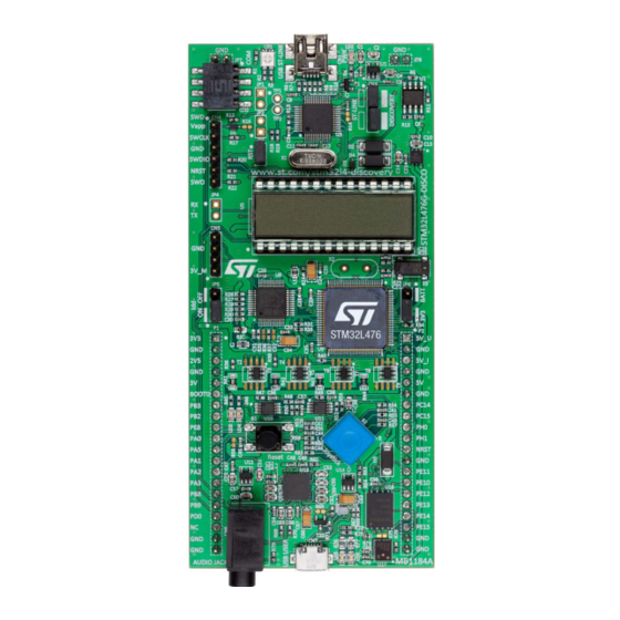
Figure 1. STM32L476 Discovery board
Picture is not contractual.
June 2018
UM1879 Rev 4
1/41
www.st.com
1
Advertisement
Table of Contents

Related Manuals for STMicroelectronics STM32L476


Summary of Contents for STMicroelectronics STM32L476
-
Page 1: Figure 1. Stm32L476 Discovery Board
User manual Discovery kit with STM32L476VG MCU Introduction The STM32L476 Discovery kit (32L476GDISCOVERY) helps the user to discover the STM32L4 ultra-low-power features and to develop and share applications. It is based on the STM32L476VGT6 microcontroller with three I Cs, three SPIs, six... -
Page 2: Table Of Contents
Contents UM1879 Contents Features ........... 6 Product marking . - Page 3 UM1879 Contents 10.11 9-axis motion sensors ........20 10.12 I C extension connector CN2 .
- Page 4 Solder bridges............23 Table 9. Typical power consumption of the STM32L476 Discovery board....36 Table 10.
- Page 5 STM32L476 Discovery board design top sheet ....... . . 25...
-
Page 6: Features
Features UM1879 Features • STM32L476VGT6 microcontroller featuring 1 Mbyte of Flash memory and 128 Kbytes of RAM in LQFP100 package • On-board ST-LINK/V2-1 supporting USB reenumeration capability • Three different interfaces supported on USB: – Virtual Com Port – Mass storage –... -
Page 7: Product Marking
Any consequences arising from such usage will not be at STMicroelectronics’ charge. In no event will STMicroelectronics be liable for any customer usage of these engineering sample tools as reference designs or in production. -
Page 8: Demonstration Software
Demonstration software UM1879 Demonstration software The demonstration software, included in the STM32Cube MCU Package corresponding to the on-board MCU, is preloaded in the STM32 Flash memory for easy demonstration of the device peripherals in standalone mode. The latest versions of the demonstration source code and associated documentation can be downloaded from the www.st.com/stm32l4- discovery web page. -
Page 9: Bootloader Limitations
UM1879 Bootloader limitations Bootloader limitations Boot from system Flash memory results in executing bootloader code stored in the system Flash memory protected against writing and erasing. This allows in-system programming (ISP), that is, flashing the STM32 user Flash memory. It also allows writing data into RAM. The data come in via one of communication interfaces such as USART, SPI, I C bus, USB or CAN. -
Page 10: Hardware Layout And Configuration
Hardware layout and configuration UM1879 Hardware layout and configuration The STM32L476 Discovery board is designed around the STM32L476VGT6 (100-pin LQFP package). The hardware block diagram (see Figure 2) illustrates the connection between the STM32L476VGT6 and the peripherals (9-axis motion sensors, digital microphone MEMS, LCD segment, 128 Mbytes of Quad-SPI Flash memory, SAI Audio DAC stereo with 3.5mm output jack, USB OTG FS, IDD current measurement, LEDs, push-button, joystick) -
Page 11: Figure 3. Stm32L476 Discovery Board Top Layout
UM1879 Hardware layout and configuration Figure 3. STM32L476 Discovery board top layout UM1879 Rev 4 11/41... -
Page 12: Figure 4. Stm32L476 Discovery Board Bottom Layout
Hardware layout and configuration UM1879 Figure 4. STM32L476 Discovery board bottom layout 12/41 UM1879 Rev 4... -
Page 13: Embedded St-Link/V2-1
In case the STM32L476 Discovery board is connected to the PC before the driver is installed, some interfaces may be declared as “Unknown” in the PC device manager. In this case the user must install the driver files, and update the driver of the connected device from the device manager. -
Page 14: St-Link/V2-1 Firmware Upgrade
To program the STM32L476VGT6 on board, simply plug in the two jumpers on CN3, as shown in Figure 6 in red, and connect the STM32L476 Discovery board to the PC through the Mini-B USB ST-LINK/V2-1 CN1 connector. Make sure the jumpers JP3, JP6.3V3, and JP5.ON are set. -
Page 15: Using St-Link/V2-1 To Program/Debug An External Stm32 Application
UM1879 Hardware layout and configuration 10.1.4 Using ST-LINK/V2-1 to program/debug an external STM32 application board To use the ST-LINK/V2-1 to program the STM32 on an external application board (out of the STM32L476VGT6 on board), remove the two jumpers from CN3 as shown in Figure 7 red, and connect the board to the CN4 software debug connector according to Table... -
Page 16: Power Supply
In case this board is powered by a USB charger or a USB battery connected on CN1, there is no USB enumeration, the led LD2 remains OFF and the STM32L476 is not powered. In this specific case only, fit the jumper JP2 to allow the STM32L476 to be powered anyway. -
Page 17: Figure 8. Board Jumper Location
UM1879 Hardware layout and configuration Figure 8. Board jumper location In this condition it is still possible to use the USB ST-LINK for communication, for programming or debugging, but it is mandatory to power supply the board first using 5V_I or USB USER CN7 then connect the USB ST-LINK cable to the PC. Proceeding this way ensures that the enumeration occurs thanks to the external power source. -
Page 18: Clock Source
Refer to Oscillator design guide for STM8S, STM8A and STM32 microcontrollers Application note (AN2867). 10.4 Reset source The reset signal NRST of the STM32L476 Discovery board is low active and the reset sources include: • The reset button B1, connected by default to NRST (SB23 closed) •... -
Page 19: User Interface: Lcd, Joystick, Leds
A green LED LD6 will be lit in one of these cases: • The power switch (U14) is ON and STM32L476 Discovery board works as a USB host • VBUS is powered by another USB host when STM32L476 Discovery board works as a USB device Red LED LD7 will be lit when an overcurrent occurs. -
Page 20: Usart Configuration
A MEMS audio sensor omnidirectional digital microphone provides a digital signal in PDM format to the STM32L476VGT6. 10.11 9-axis motion sensors STM32L476 Discovery board supports some 9-axis motion sensors, composed of: • L3GD20 (U7): a three-axis digital output gyroscope •... -
Page 21: Mcu Current Ammeter
UM1879 Hardware layout and configuration Table 6. Connector CN2 Pin number Description Pin number Description I2C1_SDA (PB7) +3V3 I2C1_SCL (PB6) EXT_RST(PD0) 10.13 MCU current ammeter The jumper JP5, labeled Idd, allows the consumption of STM32L476VGT6 to be measured directly by a built-in current ammeter circuit able to measure from 60nA to 50mA or by removing the jumper and connecting an ammeter: •... -
Page 22: Extension Connector P1 And P2
10.14 Extension connector P1 and P2 The P1 and P2 headers can connect the STM32L476 Discovery board to a standard prototyping/wrapping board. STM32L476VGT6 GPIOs are available on these connectors. P1 and P2 can also be probed by an oscilloscope, logical analyzer or voltmeter. -
Page 23: Solder Bridges
PH0, PH1 are connected to X2 crystal (X2 is not fitted) SB21, SB22 (8MHz CLK) PH0, PH1 are not connected to X2 crystal B1 push-button is connected to NRST of STM32L476 Discovery board SB23 (B1-RESET) B1 push-button is not connected to NRST of... - Page 24 Hardware layout and configuration UM1879 Table 8. Solder bridges (continued) Bridge State Description OTG_FS_VBUS signal is connected to PA9 OTG_FS_ID signal is connected to PA10 SB24, SB25 (OTG FS) OTG_FS_VBUS signal is not connected to PA9 OTG_FS_ID signal is not connected to PA10 SB26 Reserved, do not modify SB27...
-
Page 25: Schematics
Schematics Figure 10. STM32L476 Discovery board design top sheet U_LCD_GH08172 LCD_GH08172.SchDoc U_Peripherals SEG[0..23] U_STM32Lx Peripherals.SchDoc SEG[0..23] COM[0..3] STM32Lx.SchDoc COM[0..3] QSPI_CS PC14 NRST QSPI_CS PC14 NRST QSPI_CLK PC15 LD_R QSPI_CLK PC15 LD_R QSPI_D0 LD_G QSPI_D0 LD_G U_QSPI QSPI_D1 PH[0..1] JOY_CENTER QSPI_D1 PH[0..1]... -
Page 26: Figure 11. St-Link/V2-1 With Support Of Swd Only
Figure 11. ST-LINK/V2-1 with support of SWD only TCK/SWCLK PA14 SWCLK TMS/SWDIO PA13 SWDIO T_NRST NRST T_SWO 5V_IN 4K7_1%_0402 BAT60JFILM SB14 2K7_1%_0402 10K_1%_0402 100K_1%_0402 3V3_ST_LINK 10K_1%_0402 Board Ident: PC13=0 AIN_1 Not Fitted [NA] [NA] BAT60JFILM USB_RENUMn STM_JTCK T_JTCK 3V3_ST_LINK 22_1%_0402 3V3_ST_LINK SWCLK STM_JTCK... -
Page 27: Figure 12. Stm32L476Vgt6 Mcu
PB10 PD10 MFX_IRQ_OUT PC13 PB10 PD10 MFX_IRQ_OUT PB11 PD11 4K7_1%_0402 MFX_I2C_SCL PB10 PB11 PD11 MFX_I2C_SCL All this block must be very close to the STM32L476 PB12 PD12 MFX_I2C_SDA PB11 PB12 PD12 MFX_I2C_SDA PB13 PD13 4K7_1%_0402 PB13 PD13 PB14 PD14 MEMS_SCK... -
Page 28: Figure 13. Idd Measurement / Mfx (Multi Function Expander)
Figure 13. IDD measurement / MFX (Multi Function eXpander) LAYOUT PROPOSAL DRAWING 0_5%_0603 Note *: two footprints superimposed allows to 3V_MFX Ferrite 3V_MFX also populate with SO-8 package. 100nF_X7R_10%_0402 (STS9P2UH7 P MOS transistors) 1uF_POL_10%_TANA MFX_V2 GPIO0 GPIO0 SPARE SPAR A A E GPIO1 GPIO1 PC13... -
Page 29: Figure 14. Joystick Acp, Leds And Push-Button
Figure 14. Joystick ACP, LEDs and push-button Not Fitted EXT/RF E2P Connector 10K_1%_0402 SB23 I2C1_SDA LD_R NRST I2C1_SDA LD_R NRST I2C1_SCL EXT_RST 1K_1%_0402 I2C1_SCL EXT_RST LED, red LD_G LD_G SSM-104-L-DH 330_1%_0402 LED, green 100nF RESET Button COMMON USER & WAKE-UP Button 100_1%_0402 R55 10K_1%_0402 JOY_CENTER... -
Page 30: Figure 15. Lcd Display
Figure 15. LCD display SEG17 SEG16 SEG18 SEG15 SEG19 SEG14 SEG20 SEG13 SEG21 SEG12 SEG22 COM0 SEG23 COM1 U100 GH08172T SEG[0..23] SEG[0..23] COM[0..3] COM[0..3] Socket DIP28 SEG0 COM2 SEG1 COM3 SEG2 SEG11 SEG3 SEG10 SEG4 SEG9 SEG5 SEG8 SEG6 SEG7 Title: LCD Display Project:... -
Page 31: Figure 16. Otg Usb Fs
Figure 16. OTG USB FS 3V3_REG 620_1%_0603 3V3_REG 47K_1%_0402 LED, red 10K_1%_0402 PC10 FAULT OTG_FS_OverCurrent 0_5%_0402 OTG_FS_PowerSwitchOn 0_5%_0402 VBUS STMPS2141STR 4.7uF Shield PC11 USB-MICRO-AB OTG_FS_VBUS PA11 OTG_FS_DM PA12 OTG_FS_DP PC12 OTG_FS_ID 0_5%_0402 3V3_REG 330_1%_0603 Vbus D+out D+in D-out D-in LED, green 47K_1%_0402 EMIF02-USB03F2 9013-SOT23... -
Page 32: Figure 17. Audio Dac And Microphone Mems
Figure 17. Audio DAC and microphone MEMS 51_1%_0402 51_1%_0402 22nF_X7R_10%_0603 22nF_X7R_10%_0603 I2C1_SDA I2C1_SDA HP/LINE_OUTA I2C1_SCL I2C1_SCL HP/LINE_OUTB SPKR/HP SAI1_MCK 0_5%_0402 ST-225-02 SAI1_MCK MCLK SAI1_SCK SAI1_SCK SCLK SPKR_OUTA+ SAI1_SD SAI1_SD SDIN SPKR_OUTA- SAI1_FS SAI1_FS LRCK SPKR_OUTB+ AUDIO_RST AUDIO_RST RESET SPKR_OUTB- 10K_1%_0402 -VHPFILT 100nF_X7R_10%_0402 FLYN... -
Page 33: Figure 18. Quad-Spi Flash Memory
Figure 18. Quad-SPI Flash memory Quad SPI Flash Memory 10K_1%_0402 PE11 QSPI_CS QSPI_CS PE10 QSPI_CLK QSPI_CLK PE12 QSPI_D0 QSPI_D0 100nF_X7R_10%_0402 PE13 QSPI_D1 QSPI_D1 PE14 QSPI_D2 QSPI_D2 DQ2/Vpp/W# DQ2/Vpp/W PE15 QSPI_D3 QSPI_D3 DQ3/HOLD# DQ3/HOLD# N25Q128A13EF840E Title: Quad SPI Flash Memory Project: STM32L476G-DISCO Size: Reference:... -
Page 34: Figure 19. Gyroscope, Accelerometer, Magnetometer Mems
Figure 19. Gyroscope, accelerometer, magnetometer MEMS 10uF_X5R_10%_0603 VDD_IO MEMS_SCK 100nF_X7R_10%_0402 MEMS_SCK SCL/SPC MEMS_MOSI MEMS_MOSI SDA/SDI/SDO MEMS_MISO MEMS_MISO SA0/SDO GYRO_CS 10nF_X7R_10%_0603 GYRO_CS CS_I2C/SPI GYRO_INT2 GYRO_INT2 DRDY/INT2 GYRO_INT1 GYRO_INT1 INT1 L3GD20 MEMS XL_INT XL_INT MAG_DRDY MAG_DRDY MEMS_SCK XL_CS 10uF_X5R_10%_0603 XL_CS SCL/SPC INT_XL MAG_CS MAG_CS CS_XL... -
Page 35: Appendix A Power Consumption Measurements
UM1879 Power consumption measurements Appendix A Power consumption measurements The power consumption measurements of the STM32L476 Discovery board are reflected in Figure 20. Note the GPIO configuration of the STM32L476VGT6 in standby mode. Figure 20. Power consumption tree 3V3_REG Measured 287µA 287-115 =>... -
Page 36: Table 9. Typical Power Consumption Of The Stm32L476 Discovery Board
Power consumption measurements UM1879 The total measured power consumption of the STM32L476 Discovery board is 287 µA, which is as expected. Table 9 gives for each peripheral the theoretical power consumption value. It is extracted from the vendor’s product datasheet. The typical values are given under the same... -
Page 37: Appendix B Mechanical Drawing
UM1879 Mechanical drawing Appendix B Mechanical drawing Figure 21. STM32L476 Discovery board mechanical drawing UM1879 Rev 4 37/41... -
Page 38: Appendix C Compliance Statements
C.1.3 Part 15.21 Any changes or modifications to this equipment not expressly approved by STMicroelectronics may cause harmful interference and void the user’s authority to operate this equipment. IC Compliance Statement This device complies with FCC and Industry Canada RF radiation exposure limits set forth for general population for mobile application (uncontrolled exposure). -
Page 39: Déclaration De Conformité
UM1879 Compliance statements C.2.2 Déclaration de conformité Avis: Le présent appareil est conforme aux CNR d'Industrie Canada applicables aux appareils radio exempts de licence. L'exploitation est autorisée aux deux conditions suivantes : (1) l'appareil ne doit pas produire de brouillage, et (2) l'utilisateur de l'appareil doit accepter tout brouillage radioélectrique subi, même si le brouillage est susceptible d'en compromettre le fonctionnement. -
Page 40: Revision History
Revision history UM1879 Revision history Table 10. Document revision history Date Revision Changes 17-Jul-2015 Initial release. 04-Aug-2015 Added Section 6: Bootloader limitations. 24-Mar-2016 Added Section Appendix C: Compliance statements. Updated Table 8: Solder bridges. Updated Chapter 6: Ordering information. Updated Section 10.1.1: Drivers. - Page 41 IMPORTANT NOTICE – PLEASE READ CAREFULLY STMicroelectronics NV and its subsidiaries (“ST”) reserve the right to make changes, corrections, enhancements, modifications, and improvements to ST products and/or to this document at any time without notice. Purchasers should obtain the latest relevant information on ST products before placing orders.
Need help?
Do you have a question about the STM32L476 and is the answer not in the manual?
Questions and answers