Table of Contents
Advertisement
Quick Links
Advertisement
Table of Contents

Related Manuals for AXIOMTEK DASP-52282


Summary of Contents for AXIOMTEK DASP-52282
- Page 1 DASP-52282 12-bit 330KHz Multifunction w/ Free-Running Card User’s Manual...
- Page 2 Disclaimers The information in this manual has been carefully checked and is believed to be accurate. Axiomtek Co., Ltd. assumes no responsibility for any infringements of patents or other rights of third parties which may result from its use. Axiomtek assumes no responsibility for any inaccuracies that may be contained in this document.
-
Page 3: Esd Precautions
Wear a wrist-grounding strap, available from most electronic component stores, when handling boards and components. Trademarks Acknowledgments AXIOMTEK is a trademark of Axiomtek Co., Ltd. IBM is a registered trademark of International Business Machines Corporation. MS-DOS, and Windows 95/98/NT/2000 are trademarks of Microsoft Corporation. -
Page 4: Table Of Contents
2.4 A/D, D/A and DI/DO Circuits and Wiring .....17 2.5 Quick setup and test..........19 Chapter 3 Theorem of Operation .........25 3.1 Overview of DASP-52282 System Architecture and Operation ..............25 3.2 Acquisition Modes of Analog Input.....26 3.2.1 Polling Mode ............26 3.2.2 Pacer Mode............ - Page 5 4.2.15 Enable ADC Register .......... 46 4.2.16 Disable ADC Register.......... 46 Chapter 5 Calibration .............47 5.1 Calibration VR Description........47 5.2 D/A Calibration ............48 5.3 A/D Calibration Steps ...........48 Appendix A Analog Input Gain Mode Configuration ..............49 Appendix B Dimension of DASP-52282 and Accessories ................51...
- Page 6 This page does not contain any information.
-
Page 7: Chapter 1 Introduction
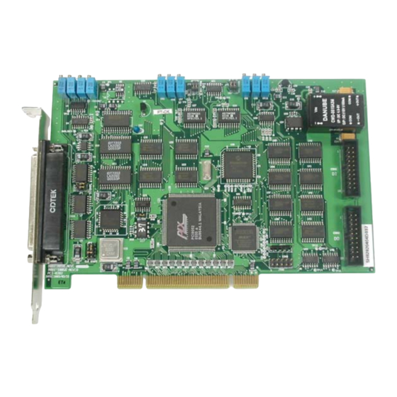
C h a p t e r 1 Introduction The DASP-52282 is a high performance, PCI bus multi- function card. It supports a 330KHz sampling rate, 16 single-ended or 8 differential AI, 16DI, and 16 DO. The DASP-52282 also features... -
Page 8: Features
VB, VC, BCB, and Delphi. And it also supports the most popular Labview 6.0/7.0 drivers. The API of the DASP-52282 has passed strict assembling tests that helps users not necessarily writer such complicated and wordy programs while using it. -
Page 9: Specifications
Resolution: 12-bit FIFO size: 1K samples Sampling Rate: 330KS/s max. Conversion Time: 3µ s ADC input range: ±10V Input protect: 30 Vp-p On chip sample and hold. Programmable Gain Low Gain (DASP-52282/ DASP-52282L only) Gain Unipolar 0~5v 0~10V 0~2.5v 0~1.25v ±10V ±5v... - Page 10 DASP-52282 Card User’s Manual AD Trigger Method: Software, Pacer, External (Pre-trigger, Post trigger, Middle trigger) Analog Input Data Transfer Method: Polling, Interrupt, FIFO Operation mode: Polling mode, Pacer mode, Interrupt mode, External pre-trigger mode, External post trigger mode, External middle trigger mode DC Accuracy: INL: +/- 1 LSB @ gain 0.5...
-
Page 11: Accessories
VOH = 2.7V min Voltage high IIH = 20 A max. @IOH =-400A max. 1.3 Accessories To make the DASP-52282 functionality complete, we carry a versatility of accessories for different user requirements in the following items: Wiring Cable CB-89037-2: 37-pin female D-sub type cable with 2m length... - Page 12 The board contains 16 channels isolated digital input which is designed for TTL level digital input signal to the DASP-52282. DB-87825: 16 relay D/O daughter board The board contains 16 channels relay output which is driven by TTL level digital output signal of the DASP-52282. Introduction...
-
Page 13: Chapter 2 Hardware Installation
DASP-52282 Card User’s Manual C h a p t e r 2 Hardware Installation 2.1 Board Layout CON1 CON2 CON4 Board Layout for DASP-52282 Hardware Installation... -
Page 14: Signal Connections
2.2 Signal Connections 2.2.1 Signal Connection Descriptions Signal Connections for DASP-52282 Referring to above figure, the accessories of the DASP-52282 are depicted and described as below. CON1: The I/O connector CON1 on the DASP-52282 is a 20-pin flat connector for digital input signals. CON1... -
Page 15: Digital Input Connector Con1
DASP-52282 Card User’s Manual 2.2.2 Digital Input Connector CON1 CON1 CB-89320 DB-87822 CON1 CB-89320 TB-88320 DI Signal Connections for DASP-52282 Hardware Installation... - Page 16 DASP-52282 Card User’s Manual CON1: Digital Input Connector Pin Assignment (20-pin Flat Connector) Description Description Digital Input 0/TTL Digital Input 1/TTL Digital Input 2/TTL Digital Input 3/TTL Digital Input 4/TTL Digital Input 5/TTL Digital Input 6/TTL Digital Input 7/TTL Digital Input 8/TTL...
-
Page 17: Digital Output Connector Con2
DASP-52282 Card User’s Manual 2.2.3 Digital Output Connector CON2 CON2 CB-89320 DB-87825 CON2 CB-89320 TB-88320 DO Signal Connections for DASP-52282 Hardware Installation... - Page 18 DASP-52282 Card User’s Manual CON2: Digital Output Connector Pin Assignment (20-pin Flat Connector) Description Description Digital Output 0/TTL Digital Output 1/TTL Digital Output 2/TTL Digital Output 3/TTL Digital Output 4/TTL Digital Output 5/TTL Digital Output 6/TTL Digital Output 7/TTL Digital Output 8/TTL...
-
Page 19: A/D, D/A And Timer/Counter Connector Con4
DASP-52282 Card User’s Manual 2.2.4 A/D, D/A and Timer/Counter Connector CON4 CON4: A/D, D/A and Timer/Counter Connector Pin Assignment CON4 CB-89037 CB-89037 TB-88037 AIO Signal Connections for DASP-52282 Hardware Installation... - Page 20 DASP-52282 Card User’s Manual D-Sub 37-pin Connector for Single-Ended Signal Description Description Analog Input 0 Analog Input 8 Analog Input 1 Analog Input 9 Analog Input 2 Analog Input 10 Analog Input 3 Analog Input 11 Analog Input 4 Analog Input 12...
- Page 21 DASP-52282 Card User’s Manual CON4: A/D, D/A and Timer/Counter Connector Pin Assignment (D-Sub 37-pin Connector for Differential Signal) Description Description Analog Input 0/+ Analog Input 0/- Analog Input 1/+ Analog Input 1/- Analog Input 2/+ Analog Input 2/- Analog Input 3/+...
-
Page 22: Jumper Setting
DASP-52282 Card User’s Manual Jumper Setting 2.3.1 ADC Clock Source (JP4) Pacer Tick Timer (8254 Counter1) External OSC Clock Cascade from Jumper Clock (8MHz) * 8254 COUT0 General Purpose Timer/Counter (8254 Counter0) Jumper External Clock OSC clock (8MHz) * 2.3.2... -
Page 23: A/D, D/A And Di/Do Circuits And Wiring
DASP-52282 Card User’s Manual 2.4 A/D, D/A and DI/DO Circuits and Wiring The analog input block diagram of DASP-52282 is depicted as in following figure. The analog input (differential and single-end input), digital input and digital output wirings are depicted as follows respectively. - Page 24 DASP-52282 Card User’s Manual 125ohms VIn+ MUX/PGA/ Analog Input Wiring Diagram for DASP-52282 (Current Input) Device Digital Input Wiring Diagram for DASP-5228 Device Digital Output Wiring Diagram for DASP-5228 Hardware Installation...
-
Page 25: Quick Setup And Test
To install a new DASP-52282 into an IBM PC compatible computer, at first, power-off the PC and open its chassis, then plug the DASP-52282 into a PCI slot. To fully benefit from the high data transfer efficiency of DASP-52282 during data acquisition, it is recommended not to install your DASP-52282 at the first PCI slot beside the AGP slot of the mainboard of PC. - Page 26 DASP-52282 Card User’s Manual Exit the PCI Configuration Utility and launch the ‘ToolWorkShop’ for DASP-52282. As shown in following. Launch ToolWorkShop Select board test Hardware Installation...
- Page 27 DASP-52282 Card User’s Manual Perform AD/DA and DIO test of DASP-52282 as shown in following. Select Test Target: DASP-52282 Hardware Installation...
- Page 28 DASP-52282 Card User’s Manual Check Device Information, Setup AO Range and Press ‘Setup’ Button to Load DASP-52282 Library Perform Analog Output Test by Set the DA Value and Measure the Output Signal of DASP-52282 by Multi-meter Hardware Installation...
- Page 29 Perform the Analog Input Test of DASP-52282. A Reference Analog Input Signal can be Connected to AI Pins of Terminal Box of DASP-52282, Press ‘ Get’ Button to Read Back AI Value. Press ‘Stop’ button to stop AD converting. Before exiting ToolWorkShop, press ‘Release’...
- Page 30 DASP-52282 Card User’s Manual This page does not contain any information. Hardware Installation...
-
Page 31: Chapter 3 Theorem Of Operation
3.1 Overview of DASP-52282 System Architecture and Operation The system block diagram of DASP-52282 is depicted as in following figure. A PCI interface to host is constructed with a PCI bridge and a 33MHz bus clock is used to drive it. In the local bus... -
Page 32: Acquisition Modes Of Analog Input
To synchronize external event and data acquisition of the DASP-52282, a series of external trigger mechanism, including pre-rigger, middle trigger and post trigger is provided. The operation mode of analog input of the DASP-52282 is described in the following subsections. 3.2.1 Polling Mode With polling mode operation, according to the user’s polling... -
Page 33: External Trigger Mode
3.2.2 and the gate control logic for the hardware pacer clock, various external trigger mode operations of DASP-52282 are realized. According to the status of consumed external trigger signal and the amount of acquired data counted by hardware logic circuit, the gate control logic of AD conversion of DASP-52282 is emulates. - Page 34 Post-Trigger Mode Principle of External Post-Trigger Operation of DASP-52282 Middle Trigger Mode For middle trigger operation, DASP-52282 acquires and keeps user-specified amount of data before the external trigger signal fired, and continues to acquire and keep data after the external trigger signal fired till the user specified amount of data is acquired.
- Page 35 Counter 1 Logic Contrller Middle Trigger Counter Tim er Counter 2 External Trigger Functional Block Diagram of Middle-Trigger of DASP-52282 Convert Counter: N = N1 + N2 External Trigger Signal N2: Middle-Trigger Counter User Start Analog Signal Convert Start Convert Stop...
-
Page 36: Double Buffering Mechanism For Fast Data Acquisition
The FIFO HF IRQ in the host is dispatched to the ring 0 driver of DASP-52282, and a batch data transfer mechanism is launched to transfer the acquired data in on board FIFO of DASP-52282 to host, as show in following figure. - Page 37 DASP-52282 Card User’s Manual software buffer host computer PCI Bus DASP-52282 Notification On board FIFO N+X+1 N+X+2 Principle of HF Interrupt Driven Massive Data Transfer of DASP-52282 Theorem of Operation...
-
Page 38: Circular Buffer For Massive Data Buffering
To achieve the desired double buffering mechanism for DASP-52282, a 256K word ring 0 software buffer is constructed by the ring 0 driver of DASP-52282. The ring 0 software buffer serves as the second data buffer for massive data transfer between DASP-52282 and host computer. -
Page 39: Analog Input Range, Adc Code And Ad Value
DASP-52282, the nonlinearity of this linear mapping is described in section 1.2. Figure 4-6 depicts the linear mapping of AD code of DASP-52282 and the analog input signal. FS denotes the full span of analog input under the user configured analog input range. - Page 40 0~10V 0xFFF/4095 0x0/0 1LSB ±00.000 +4.99878 0.00122V 0~5V 0xFFF/4095 0x0/0 1LSB ±00.000 +2.49939 0.00061V 0~2.5V 0xFFF/4095 0x0/0 1LSB ±00.000 +1.249695 0.000305 0~1.25V 0xFFF/4095 0x0/0 1LSB Input Range, Data/Code and Resolution of DASP-52282 / DASP-52282L – Uni-Polar Input Theorem of Operation...
- Page 41 DASP-52282 Card User’s Manual Input -Full Data +Full Scale Zero Range Scale Resolution ±00.000 +9.99512 -10.000 0.00488V ±10V 0xFFF/4095 0x800/2048 0x0/0 1LSB ±00.000 +4.99756 -5.000 0.00244V ±5V 0xFFF/4095 0x800/2048 0x0/0 1LSB ±00.000 +0.499756 -0.5 0.000244V ±0.5V 0xFFF/4095 0x800/2048 0x0/0 1LSB ±00.000...
- Page 42 DASP-52282 Card User’s Manual This page does not contain any information. Theorem of Operation...
-
Page 43: Chapter 4 Register Structure And Format
C h a p t e r 4 Register Structure and Format 4.1 Overview The DASP-52282 board occupies 16 consecutive I/O address. The address of each register is defined as the board’s base address plus an offset. The I/O registers and their corresponding functions are listed in the followings. -
Page 44: I/O Register Map
DASP-52282 Card User’s Manual 4.2 I/O Register Map 4.2.1 Digital Input Buffer Register Read (Base Address + Offset 0x00-01) Digital Input Low Byte (D0-D7) Digital Input High Byte (D8-D15) 4.2.2 Digital Output Latch Register Write (Base Address + Offset 0x00-01) - Page 45 DASP-52282 Card User’s Manual General Status Buffer Register is used to check the A/D activity. The format is described as bellows. EF: (Bit 0 = 0) FIFO is Empty HF: (Bit 1 = 0) FIFO is Half-Full FF: (Bit 2 = 0) FIFO is Full...
-
Page 46: Command Output Latch Register
DASP-52282 Card User’s Manual 4.2.4 Command Output Latch Register Write (Base Address + Offset 0x02-03) MUX3 MUX2 MUX1 MUX0 HDSK Mode2 Mode1 Mode0 DevID Ref1 Ref0 Gain1 Gain0 CMDOK Command Output Latch Register is used to set the A/D operation. - Page 47 DASP-52282 Card User’s Manual Single-Ended mode channel selection Channel MUX3 MUX2 MUX1 MUX0 Ch10 Ch11 Ch12 Ch13 Ch14 Ch15 Differential mode channel selection Channel MUX2 MUX1 MUX0 MUX3: Don’t care bit in differential mode. Registry Structure and Format...
- Page 48 DASP-52282 Card User’s Manual Gain0-1: A/D Gain Control (PGA205 or PGA206) A/D GAIN Gain0 Gain1 Ref0-1: A/D Reference Control Instrumentation Gain Ref0 0.5x Offset Ref1 Registry Structure and Format...
-
Page 49: A/D Data Register
DASP-52282 Card User’s Manual 4.2.5 A/D Data Register Read (Base Address + Offset 0x04-05) AD Data (D0-D11) Reserved AD Data (D0-D11) 4.2.6 DAC Channel 1 Output Latch Register Write (Base Address + Offset 0x04-05) DA Data to Channel 1 (D0-D11) -
Page 50: Dac Channel 2 Output Latch Register
DASP-52282 Card User’s Manual 4.2.8 DAC Channel 2 Output Latch Register Write (Base Address + Offset 0x06-07) DA Data to Channel 2 (D0-D11) DA Data to Channel 2 Reserved (D0-D11) 4.2.9 8254 Timer/Counter Register Read/ Write (Base Address + Offset 0x08-0C) 8254 Counter 0, 1, and 2 Please refer to Intel’s “Micro-system Components Handbook”... -
Page 51: Clear Fifo Content Register
DASP-52282 Card User’s Manual 4.2.11 Clear FIFO Content Register Write (Base Address + Offset 0x10) Write Any Value to Clear FIFO Content Reserved 4.2.12 Clear Flag Register Write (Base Address + Offset 0x12) Write Any Value to Reset the System Status to Initial State Reserved 4.2.13... -
Page 52: A/D Adc Software Polling Control Register
DASP-52282 Card User’s Manual 4.2.14 A/D ADC Software Polling Control Register Write (Base Address + Offset 0x16) Write Any Value to Generate an AD Conversion Signal Reserved Write this register to any value to generate a Conversion Signal and the PReady Bit (Status Register Bit 3) will be set to TRUE. -
Page 53: Chapter 5 Calibration
C h a p t e r 5 Calibration 5.1 Calibration VR Description There are ten variable resistors (VR) on the DASP-52282 to adjust the A/D and D/A channels. A precision voltmeter with 4 1/2 digits should be used to take an accurate voltage reference. A calibration program can be found on the DASP-52282 software disk to perform the calibration steps. -
Page 54: D/A Calibration
DASP-52282 Card User’s Manual 5.2 D/A Calibration Calibration procedure is easily performed by using the calibration program. Step-by-step walkthrough of D/A calibration is listed as follows: Select DAC1 (JP8) and DAC2 (JP9) to ±10V output range Set DAC1 and DAC2 output data to -10V and adjust VR5, VR8 until DAC1 and DAC2 output voltage to -10V with 1 LSB tolerance (±2.44mV) -
Page 55: Appendix A Analog Input Gain Mode Configuration
DASP-52282 Card User’s Manual A p p e n d i x A Analog Input Gain Mode Configuration Command Register Gain Input Full High Byte bit11~ bit8 Gain Type Mode Range Range Ref1 Ref0 Gain1 Gain0 ±5V Bipolar ±2.5V Bipolar ±1.25V... - Page 56 DASP-52282 Card User’s Manual This page does not contain any information. Analog Input Gain Mode Configuration...
-
Page 57: Appendix B Dimension Of Dasp-52282 And Accessories
DASP-52282 Card User’s Manual A p p e n d i x B Dimension of DASP-52282 and Accessories DASP-52282 TB-88037 Dimension of DASP-52282 and Accessories... - Page 58 DASP-52282 Card User’s Manual TB-88320 DB-87822 Dimension of DASP-52282 and Accessories...
- Page 59 DASP-52282 Card User’s Manual DB-87825 Dimension of DASP-52282 and Accessories...
Need help?
Do you have a question about the DASP-52282 and is the answer not in the manual?
Questions and answers