
Subscribe to Our Youtube Channel
Related Manuals for Dalsa 1M28-SA


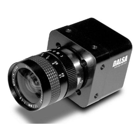
Summary of Contents for Dalsa 1M28-SA
- Page 1 1M28-SA 1M75-SA 1M150-SA One Megapixel CMOS Stop Action Camera Family Camera User’s Manual 03-32-00525 rev 04 Printed 09/30/03 11:21 AM...
- Page 2 1M28, 1M75, and 1M150 User’s Manual © 2003 DALSA. All information provided in this manual is believed to be accurate and reliable. No responsibility is assumed by DALSA for its use. DALSA reserves the right to make changes to this information without notice.
-
Page 3: Table Of Contents
Software Interface: Controlling the Camera _____________________________________ 35 3.1 Overview ..................................35 3.2 PFRemote Configuration Tool .............................36 3.3 Modifying Camera Registers ............................38 3.4 Register Descriptions ..............................39 3.5 Register Assignment and Instruction Set of the ADC-Module..................46 3.6 Instructions for Control of the ADC-Module.........................47 DALSA 03-32-00525-04... - Page 4 5.1 Protecting Against Dust, Oil and Scratches ........................51 5.2 Cleaning the Sensor Window............................51 Configuration Settings of the EEPROM Sensor ___________________________________ 53 Asynchronous Communications (Camera Link) Interface ____________________________ 61 Accessing the EEPROM____________________________________________________ 65 Pseudo Random Number Generator __________________________________________ 69 Index _______________________________________________________________ 73 03-32-00525-04 DALSA...
-
Page 5: Introduction To The 1M28, 1M75, And 1M150 Family
Programmable features include: gain, offset, line rates, trigger mode, test pattern output, and camera diagnostics. • DLLs for integrating camera control functions into your system. The DLLs require a framegrabber that has a virtual COM port, or a COM port input. DALSA 03-32-00525-04... -
Page 6: Image Sensor
48dB linear (8bit); 120dB LinLog2 Quantum Efficiency 25% (including fill factor) Exposure Time 1 µs—0.5s in steps of 35ns Sensitivity 10 µJ/m /LSB @630 nm, 8 bit Spectral Range 400 - 800nm Number of outputs 1 or 4 03-32-00525-04 DALSA... - Page 7 All tests conducted with gain off and skimming off with QTH lamp (color temp. 3200K) with Wide Band Hot Mirror (750nm cutoff). Exposure time set to 10ms. Camera operating in linear mode. Camera operating under 25°C ambient temperature. DALSA 03-32-00525-04...
-
Page 8: Hot Pixels
7DN. Figure 2: Typical Output at Dark, 10ms Exposure Time Figure 2 depicts the number of pixels that generate larger amounts of dark current than your average pixel—the average pixel level output is 8DN. 03-32-00525-04 DALSA... - Page 9 Dark blemishes are areas of the sensor where the pixel(s) are not as responsive as the average pixel. Dark blemishes can be isolated single pixel defects, but can also be found in clusters. Figure 3 and Figure 4 show the distribution of dark blemishes. DALSA 03-32-00525-04...
-
Page 10: Spectral Responsivity
IR Band. For classical visible applications, consider the use of IR stop filters to increase the sharpness of the images since commercial lenses often cannot provide proper focalization over such a large spectrum. Figure 6: Quantum Efficiency as a Function of Wavelength 03-32-00525-04 DALSA... -
Page 11: Camera Performance Specifications
(rms), max 350:1 Skimming on, Gain off 350:1 Skimming off, Gain on ~16x 196:1 Skimming on, Gain on RMS Noise, max Skimming off, Gain off Skimming on, Gain off Skimming off, Gain on ~16x 1.25 Skimming on, Gain on DALSA 03-32-00525-04... -
Page 12: Camera Operating Modes Overview
Turns image upside down. See section 1.11 Flip Image Mode for details. 8bit Camera delivers 8 bit data (Gray levels 0...255). LFSR Linear-Feedback-Shift-Register: Generates a pseudo-random image so errors can be identified in the complete image processing system. See Appendix D 03-32-00525-04 DALSA... -
Page 13: Pixel Response: Linear And Linlog Modes
LinLog technology further overcomes image lag, or ghost images related to the slow response speed of pure logarithmic sensors. The LinLog response is best suited for applications with uncontrolled DALSA 03-32-00525-04... - Page 14 A family of measured characteristic curves is shown in Figure 8. The COMP ratio has a strong influence on the resulting signal. Figure 10: Parameter adjustment procedure for LL2 shows a flowchart for help with optimization. 03-32-00525-04 DALSA...
- Page 15 The value LL1 must be greater than LL2. Values (LL1, LL2) larger than 80.1 cause the picture quality to be degraded. Setting values larger than 81.3 no longer influence the characteristic curve significantly (Figure 3). In this case, unwanted effects like offset between the two fields are possible. DALSA 03-32-00525-04...
- Page 16 (the A/D converter is out of range) because the logarithmic compression is only effective on the upper intensity values. If it is necessary to use a camera with a logarithmic response curve, the LinLog technology will not replace it completely. On demand, DALSA cameras can be modified to fulfil these needs.
- Page 17 < Gray scale 200 gravity of histogram Phase 2 Rough setting for COMP Initial value = 5 Take a picture decrease increase COMP COMP Is the contrast in the overexposed areas acceptable ? too low too high Phase 3 DALSA 03-32-00525-04...
- Page 18 Is the contrast in the overexposed areas acceptable ? too high too low Black adjust Phase 4 Fine adjustment of COMP Black adjust Phase 5 Adjustment of characteristics using LUT, optimized for the application's gray scale output: 8 Bit 03-32-00525-04 DALSA...
-
Page 19: Gain Response: Skim And High Gain Modes
Skimming Gain 1x or 4x 1x or 4x Note: In skimming mode increased responsivity results in a nonlinear output. Note: Gain values are set using the PFRemote configuration tool. See chapter 3 for details on using the PFRemote. DALSA 03-32-00525-04... -
Page 20: Region Of Interest (Roi Mode)
The only restriction (see the note below to deactivate this restriction) is that at least 64 pixels must be activated symmetrically on both halves of the sensor in the x-direction. In the y-direction, you can set any non-zero number of lines. Having satisfied this 03-32-00525-04 DALSA... - Page 21 ROI, Line pause = 8 valid ROI, Line pause = 8 EN_PRELOAD = 1 EN_PRELOAD = 1 (0,0) (0,0) valid ROI, Line pause = 32 valid ROI, Line pause = 8 EN_PRELOAD = 0 EN_PRELOAD = 1 (0,0) (0,0) >64 Pixels DALSA 03-32-00525-04...
-
Page 22: Mask Mode (Mroi)
Unused ROI pairs must be filled with the maximum value 3FF for both start and stop values. The final ROI is terminated with the parameter Y1_ROI. The arrangement of the various parameters is shown graphically in Figure 17. 03-32-00525-04 DALSA... -
Page 23: Line Hopping Mode
Another possible way to increase the image data rate is to jump over lines (Line Hopping). In Line Hopping mode, the camera delivers a pseudo-image to the framegrabber consisting of the composition of individual selected lines. The 1MXXX camera family allows you to define the DALSA 03-32-00525-04... -
Page 24: Flip Image Mode
• Frame rate is the reciprocal of frame time. • With an external MCLK, the time unit t must match the frequency used. • More information on calculating frame rates is available at http://vfm.dalsa.com/support/faqs/faqs.asp. 03-32-00525-04 DALSA... -
Page 25: Camera Hardware Interface
1. Connect Camera Link™ cables from camera to framegrabber. 2. Connect power. You must also set up the other components of your system, including light sources, framegrabbers, camera mounts, heat sinks, host computers, optics, encoders, and so on. See section 2.1 above for camera configuration information. DALSA 03-32-00525-04... -
Page 26: Input/Output
Linear Linear Linear Gain Resolution Full-resolution, 1024 x Full-resolution, 1024 x Full-resolution, 1024 x 1024 1024 1024 Exposure time 10 ms 12 ms 20 ms Frame rate 20 fps 25 fps 20 fps Data rate 28MHz 2x40MHz 2x80MHz 03-32-00525-04 DALSA... -
Page 27: Connectors
SerTC+ SerTC- SerTFG- SerTFG+ CC1- CC1+ CC2+ CC2- CC3- CC4+ inner shield inner shield Table 8: DALSA Camera Control Configuration Signal Configuration EXSYNC 9, 22 External Master Clock 10, 23 PRIN (Exposure Control) 11, 24 Not Used 12, 25 DALSA... - Page 28 Data bit CameraLink Port and bit LSB +1 LSB +2 LSB +3 LSB +4 LSB +5 LSB +6 LSB +7 Figure 18: 1M75 and 1M150 Camera to Sensor Pixel Map Camera tap assignment Sensor tap assignment (0,0) (0,0) 03-32-00525-04 DALSA...
-
Page 29: Power Supplies
These signals indicate when data is valid, allowing the data to be clocked from the camera to your acquisition system. These signals are part of the Camera Link configuration. Refer to the DALSA Camera Link Implementation Road Map, available at http://vfm.dalsa.com, for the standard... -
Page 30: Timing
Note: The reset time is small, at 1-2µs. Figure 19: External Trigger Mode, Constant Image Data Rate Ignored Exsync Exsync Integration Readout Reset Integration Frame Timer Figure 20: External Trigger Mode, Variable Image Data Rate Integration Reset Integration Readout 03-32-00525-04 DALSA... -
Page 31: Freerunning Mode
The signals FRAME_VALID (FVAL) and LINE_VALID (LVAL) mask valid image information. The number of clock pixels after exposure CPRE is defined by the calculation of the frame time (see section 1.12 Calculating Frame Rate). DALSA 03-32-00525-04... - Page 32 The data is output on the rising edge of the pixel clock. The signals FRAME_VALID (FVAL) and LINE_VALID (LVAL) mask valid image information. The number of clock pulses after exposure CPRE is defined by the calculation of the frame time (see section 1.12 Calculating Frame Rate). 03-32-00525-04 DALSA...
- Page 33 The integration ends with the rising edge of the external signal PRIN. The signals EXSYNC and PRIN are clocked in the sensor control in such a way that the internal exposure control becomes active one clock later. DALSA 03-32-00525-04...
-
Page 34: Dummy Test Row
If the data read out from the sensor is not within the ADC conversion range (over or under exposed), the LED changes to red while the saturated data is read out. • The status LED changes to red while the serial communication is active. 03-32-00525-04 DALSA... -
Page 35: Software Interface: Controlling The Camera
You can also configure the camera through the PFLIB application programming interface. For more information, refer to page 48. Camera Serial Port Defaults • 8 data bits • 1 start bit • 1 stop bit • No parity • 9.6Kbps DALSA 03-32-00525-04... -
Page 36: Pfremote Configuration Tool
Unzip the 1M28_1M75_1M150_PFRemote_Software.zip and copy the files contained in the zip file to a directory on your computer. Alternately, the latest version of the software is also available at http://vfm.dalsa.com/docs/docs.asp in the “Software” folder. Opening PFRemote Before running PFRemote, make sure that you have installed your framegrabber and framegrabber software. - Page 37 To configure the camera: In PFRemote, open a connection with the camera. For details on opening a connection with your camera, see Opening PFRemote on page 36. Right click on the camera name and select Configure. The configuration dialog box opens: DALSA 03-32-00525-04...
-
Page 38: Modifying Camera Registers
PFRemote.exe. Refer to Saving and Loading EEPROM Settings on page 37 for further information on the PFRemote. We also recommend that you do not alter the custom calibration settings available through the calibration dialog box (Camera → Calibration). Consult DALSA support at support@dalsa.com before altering calibration values. -
Page 39: Register Descriptions
0 – 2 are sent to the EEPROM Command RELOAD of the registers / Status register has 3 internal states Status register 4 internal states Mode register 0 , adjust camera modes Mode register 1 , adjust camera modes DALSA 03-32-00525-04... - Page 40 Line pause Interlacing 34-46 22-2E Not Used Choice of a RAM bank for read/write access Byte 0 of a 16x8 RAM-Bank Byte 1 of a 16x8 RAM-Bank Byte 2 of a 16x8 RAM-Bank Byte 3 of a 16x8 RAM-Bank 03-32-00525-04 DALSA...
- Page 41 ! No write operations to EEPROM allowed! PROM_BUSY, ! No write operations to EEPROM allowed ! always 0 sensor module ERROR_NO_EXSYNC, timeout digital mono flop ERROR_NO_EXPOSURE, timeout digital mono flop ERROR_NO_MCLK, timeout digital mono flop Not used = 0 Not used = 0 DALSA 03-32-00525-04...
- Page 42 Bit 4 activates the automatic switching of the camera’s LinLog and Skim factory settings to predefined LinLog and Skim settings. It also controls automatic offset compensation when switching to a high gain (bit7 register 7) and the activation of the classical logarithmic mode (bit 6 03-32-00525-04 DALSA...
- Page 43 1 WARNING: Do not modify Mode Register 1 (bits 0 to 3). If corruption occurs, write in default values or contact DALSA. Modifying these values may result in a malfunction or limited functioning of the camera. You should use the LSFR test pattern for data path integrity. Alternately, you can turn on the dummy line with bit 4.
- Page 44 EXPOSURE signal EN_SYNC_EXPOSURE External triggering and integration control by EXPOSURE signal, integration begins on positive edge of EXPOSURE signal and EXSYNC is on, integration ends on negative edge of EXPOSURE Signal POLARITY_SYNC_EXP SYNC_EXPOSURE active HIGH i.e. rising 03-32-00525-04 DALSA...
- Page 45 1M28, 50ns for 1M75, and 25ns for 1M150). The frame time is used to keep the frame rate NOTE: The frame rate sets the maximum exposure constant, independent of the exposure time. time. Invalid values must be prevented via software. DALSA 03-32-00525-04...
-
Page 46: Register Assignment And Instruction Set Of The Adc-Module
LUT of the ADC module are accessible. After accessing the ADC module, the camera must be reset to slave mode, where the external clock is used. 03-32-00525-04 DALSA... -
Page 47: Instructions For Control Of The Adc-Module
AUTOLOAD state (after power-on or reset of the camera), the settings are being copied from the During this phase, EEPROM access is not permitted Incorrect EEPROM to the internal registers. information will corrupt the internal camera register. The PROM_BUSY state indicates an DALSA 03-32-00525-04... -
Page 48: Pflib Api Commands
It contains all of the files necessary to use the PFLIB API commands, including documentation. Unzip the 1M28_1M75_1M150_PFRemote_Software.zip and copy the files contained in the zip file to a directory on your computer. Alternately, the latest version of the software is also available at http://vfm.dalsa.com/docs/docs.asp in the “Software” folder. 03-32-00525-04 DALSA... -
Page 49: Optical And Mechanical Considerations
Optical and Mechanical Optical and Mechanical Optical and Mechanical Optical and Mechanical Considerations Considerations Considerations Considerations 4.1 Mechanical Interface Figure 31: Camera Dimensions 38.1 10.45 0.75 1” 1/32st ø12 ø3 ø6.10 ø6 3.45 34.65 51.0 ø1/4” All units in mm. DALSA 03-32-00525-04... -
Page 50: Optical Interface
The cameras come with a built in C-mount lens adapter with the appropriate back focal distance (17.52 ±0.18mm). 4.3 Compliance The IM28, 1M75, and 1M150 have passed the following EMC tests: • EN 61000-6-3: 2001 • EN 61000-6-2: 2001 03-32-00525-04 DALSA... -
Page 51: Sensor Handling Instructions
The location of these pixels changes with the angle of illumination. 5.2 Cleaning the Sensor Window 1. Use compressed air to blow off loose particles. This step alone is usually sufficient to clean the sensor window. DALSA 03-32-00525-04... - Page 52 3. Wipe the window carefully and slowly. 4. When cleaning long linear sensors, it may be easier to wipe along the width (i.e. as opposed to the length) of the sensor. 03-32-00525-04 DALSA...
-
Page 53: Configuration Settings Of The Eeprom Sensor
The storage addresses 500H – 6FFH are reserved for camera control variables. Details can be found in the software manual. The area 700H – 7FFH is reserved. In the event of queries or service requests, a dump of the EEPROM contents should be sent to DALSA together with an error description. DALSA 03-32-00525-04... - Page 54 (**) Chan0_Main_LSB LSB DAC0 Channel 0 Main register (**) Chan0_Main_MSB MSB DAC0 Channel 0 Main register (**) Chan0_Sub_LSB LSB DAC0 Channel 0 Sub register (**) Chan0_Sub_MSB MSB DAC0 Channel 0 Sub register (**) Chan1_Main_LSB LSB DAC0 Channel 1 03-32-00525-04 DALSA...
- Page 55 LSB DAC0 Channel 6 Main register (**) Chan6_Main_MSB MSB DAC0 Channel 6 Main register (**) Chan6_Sub_LSB LSB DAC0 Channel 6 Sub register (**) Chan6_Sub_MSB MSB DAC0 Channel 6 Sub register (**) Chan7_Main_LSB LSB DAC0 Channel 7 Main register DALSA 03-32-00525-04...
- Page 56 MSB ROI-X1 Matrix sensors ( Y1_ROI[7:0] LSB ROI-Y1 Matrix sensors Y1_ROI[15:8] MSB ROI-Y1 Matrix sensors ( LINE_PAUSE[7:0] Line pause LINE_JUMP[7:0] Line jump Not used Not used Not used Not used Not used Not used Not used Not used 03-32-00525-04 DALSA...
- Page 57 LSB stop value 7 BANK1_BYTE8[7:0] LSB stop value 8 BANK1_BYTE9[7:0] LSB stop value 9 BANK1_BYTE10[7:0] LSB stop value 10 BANK1_BYTE11[7:0] LSB stop value 11 BANK1_BYTE12[7:0] LSB stop value 12 BANK1_BYTE13[7:0] LSB stop value 13 BANK1_BYTE14[7:0] LSB stop value 14 DALSA 03-32-00525-04...
- Page 58 MSB start value 5 (*) BANK4_BYTE6[1:0] MSB start value 6 (*) BANK4_BYTE7[1:0] MSB start value 7 (*) BANK4_BYTE8[1:0] MSB start value 8 (*) BANK4_BYTE9[1:0] MSB start value 9 (*) BANK4_BYTE10[1:0] MSB start value 10 (*) BANK4_BYTE11[1:0] MSB start value 11 (*) 03-32-00525-04 DALSA...
- Page 59 MSB DAC0 Channel 4 Main register Base + 12 LSB DAC0 Channel 4 Sub register Base + 13 MSB DAC0 Channel 4 Sub register Base + 14 LSB DAC0 Channel 5 Main register Base + 15 MSB DAC0 Channel 5 Main register DALSA 03-32-00525-04...
- Page 60 MSB DAC0 Channel 6 Sub register Base + 1C LSB DAC0 Channel 7 Main register Base + 1D MSB DAC0 Channel 7 Main register Base + 1E LSB DAC0 Channel 7 Sub register Base + 1F MSB DAC0 Channel 7 Sub register 03-32-00525-04 DALSA...
-
Page 61: Asynchronous Communications (Camera Link) Interface
When data or addresses are written (WRITE Mode), the RS232 interface of the camera answers with ACK = 06H if the transfer was successful, or with NAK = 15H if the transfer failed. Therefore, it is possible to control the complete transfer process by the software. When a register is DALSA 03-32-00525-04... -
Page 62: Example Of Access To Camera Registers
1100 1010 Write High Data Nibble A 0000 0110 Successful receipt, camera transmits ACK = 0000 0110 Read Data from register address 6 0101 0101 camera transmits register content address 0000 0111 Read data from register address 7 03-32-00525-04 DALSA... - Page 63 1M28, 1M75, and 1M150 User’s Manual PRELIMINARY Steps RX/TX BIN Code Comments Code 1010 1010 camera transmits register content address 0001 0111 Read data from undefined register address 0001 1000 camera transmits CAN = 18H; not allowed or undefined DALSA 03-32-00525-04...
- Page 64 PRELIMINARY 1M28, 1M75, and 1M150 User’s Manual 03-32-00525-04 DALSA...
-
Page 65: Accessing The Eeprom
Register address 2 – ADDR_MSB_EEPROM Name Description ADDR_MSB_EEPROM Address bit 8 ADDR_MSB_EEPROM Address bit 9 / OP-Code bit 0 ADDR_LSB_EEPROM Address bit 10 / OP-Code bit 1 ADDR_LSB_EEPROM OP-Code bit 2 ADDR_LSB_EEPROM OP-Code bit 3 Not used Not used Not used DALSA 03-32-00525-04... -
Page 66: Example Of Eeprom Access
Read status register address 04H, wait for state „not (PROM_BUSY or AUTOLOAD)“ Read databyte (D7-D0) in register address 00H, when data are read out from the EEPROM The following example shows in detail the sequence of commands for the EEPROM command write enable. 03-32-00525-04 DALSA... - Page 67 Address 04H 0000 0100 Read status register from register address 04H 01xx xxxx Write to address xx00 0011 Address 03H 0100 0011 Command SEND_PROM, Data will be transmitted to the EEPROM These steps are not required arbitrary state DALSA 03-32-00525-04...
- Page 68 PRELIMINARY 1M28, 1M75, and 1M150 User’s Manual 03-32-00525-04 DALSA...
-
Page 69: Pseudo Random Number Generator
1000101011 1101011001 53 0111111011 85 0001110001 117 2A3 1100010101 1110101100 54 2FC 0011111101 86 1000111000 118 147 1110001010 1AF 1111010110 55 0001111110 87 0100011100 119 28F 1111000101 35F 1111101011 56 3F0 0000111111 88 1C4 0010001110 120 11E 0111100010 DALSA 03-32-00525-04... - Page 70 156 2AF 1111010101 188 1AC 0011010110 220 0AA 0101010100 252 1C2 0100001110 157 15E 0111101010 189 359 1001101011 221 154 0010101010 253 384 0010000111 158 2BD 1011110101 190 2B3 1100110101 222 2A9 1001010101 254 308 0001000011 159 17A 0101111010 191 167 1110011010 223 153 1100101010 255 211 1000100001 03-32-00525-04 DALSA...
- Page 71 (ICLK'event and ICLK='1') then if (RESET = '1') then reset:shift register is loaded with 1. REG <= "0000000001"; else REG <= REG(8 downto 0) & DATAIN; end if; end if; end process SR10R; DATAIN <= REG(2) xor REG(9); LFSR_OUT <= REG; DALSA 03-32-00525-04...
- Page 72 PRELIMINARY 1M28, 1M75, and 1M150 User’s Manual 03-32-00525-04 DALSA...
-
Page 73: Index
Index Index Index loading settings, 37, 38 programming, 65 A A A A saving settings, 37, 38 storage functions, 53 about DALSA, 2 EEPROM control, 41 ADC module, 46 EMC compliance, 50 amplification, 19 EXRCLK, 29 application programming EXSYNC, 29... - Page 74 Q Q Q Q frame, 30 global shutter, 31 quantum efficiency, 10 triggered, 32 triggered mode, 32 R R R R V V V V randomnumber generator, 69 recover factory settings, 37 VDHL, 71 region of interest (ROI), 20 register adjustment 03-32-00525-04 DALSA...
Need help?
Do you have a question about the 1M28-SA and is the answer not in the manual?
Questions and answers