
Related Manuals for Freescale Semiconductor MPC8272ADS


Summary of Contents for Freescale Semiconductor MPC8272ADS
- Page 1 MPC8272ADSUG 3/2004 Rev. 0.1 MPC8272ADS User Guide This datasheet has been downloaded from http://www.digchip.com at this page...
- Page 2 Technical Information Center or for any other application in which the failure of the Freescale Semiconductor product Schatzbogen 7 could create a situation where personal injury or death may occur. Should Buyer...
-
Page 3: Table Of Contents
Title Title Number Number Contents About This Book Chapter 1 Overview MPC8272ADS Specifications ................1-1 MPC8272ADS Features ..................1-2 Chapter 2 Hardware Preparation and Installation Unpacking Instructions ..................2-1 Hardware Preparation ..................2-1 2.2.1 Setting the Supply Voltage Level............2-3 VDDL 2.2.2... - Page 4 3.1.1 Host-Controlled Operation ................3-1 3.1.2 Stand Alone Operation..................3-2 3.1.3 COP/JTAG Connector—P21 ................3-3 3.1.4 Terminal to MPC8272ADS RS-232 Connection..........3-3 3.1.5 10/100-Base-T Ethernet Ports Connection ............3-4 3.1.6 Memory Installation..................3-4 3.1.6.1 Flash Memory SIMM Installation ............... 3-4...
- Page 5 Contents Paragraph Page Number Title Number 4.1.30 Fast Ethernet Port 2 Full Duplex Indicator—LD6........... 4-6 4.1.31 General Purpose Led 1 Indicator—LD25............4-6 4.1.32 Fast Ethernet Port 2 100Base-Tx Indicator—LD7 .......... 4-6 4.1.33 USB Enabled Indicator—LD21............... 4-6 4.1.34 Ethernet Port 2 LINK Indicator—LD9............4-7 4.1.35 Ethernet Port 2 Tx/Rx Indicator—LD8 ............
- Page 6 5-V Standby Rail ..................... 7-3 7.1.4 Rail ......................7-3 7.1.4.1 Bus..................... 7-3 7.1.4.2 12-V Rail ..................... 7-4 7.1.4.3 -12-V Rail ....................7-4 Connectors ......................7-4 7.2.1 ATX Power Connector..................7-4 7.2.2 Fast Ethernet Port Connectors ................. 7-4 MPC8272ADS User Guide...
- Page 7 Contents Paragraph Page Number Title Number 7.2.3 ATM 155 Port Connection................7-5 7.2.4 RS232 Port Connector ..................7-5 7.2.5 CPM Expansion Connector ................7-5 7.2.6 COP/JTAG Port Connector................7-5 7.2.7 Logic Analyzer Connectors ................7-5 7.2.8 Mach’s In System Programming (ISP) Connector .......... 7-5 7.2.9 PCI Connectors ....................
- Page 8 Contents Paragraph Page Number Title Number MPC8272ADS User Guide...
- Page 9 Page Number Title Number Figures MPC8272ADS Block Diagram................... 1-4 MPC8272ADS Top Side Part Location Diagram ............2-2 Trimmer—RP1 ....................2-3 SW5 Description ......................2-4 Hard Reset Configuration Source Selection—JP9............2-5 SW2 Description ......................2-6 Clock Source Selection ....................2-7 FCC1 Ethernet Mode Selection .................. 2-7 FCC2 Ethernet Mode Selection ..................
- Page 10 Figures MPC8272ADS User Guide...
- Page 11 BCSR5 to BCSR7 Description ................. 5-33 5-20 COP/JTAG Port Signals Description ................ 5-34 MPC8272ADS Memory Map—Flash (or BCSR) as Boot Device......6-1 MPC8272ADS Memory Map—E2PROM as Boot Device........6-3 BCSR/Flash Power On Reset Configuration .............. 6-6 E2PROM Power On Reset Configuration ..............6-6 SIU Register Programming ..................
- Page 12 Title Number P16—COP/JTAG Connector ..................8-2 P1—CPM Expansion Connector ................8-4 P26, P28, P29—PCI Connectors................8-13 P31—ATX Power Supply Connector ............... 8-15 P3—Lattice ISP Connector ..................8-16 P2—System Expansion Connector ................8-17 P16, P19—USB Connectors ..................8-22 MPC8272ADS User Guide...
- Page 13 The primary objective of this manual is to describe the functionality of the MPC8272ADS board. It contains operational, functional and general information about the MPC8272ADS.
- Page 14 Organization The following list describes the major sections of this manual: • Chapter 1, “Overview,” provides a high-level description of the MPC8272ADS, describing general operation, basic features, and a block diagram. • Chapter 2, “Hardware Preparation and Installation,” provides unpacking instructions and information about setting various modes, switches, and other configuration on the MPC8272ADS.
- Page 15 MPC8272 Documentation Supporting documentation for the MPC8272 can be accessed through the world-wide web www.motorola.com/semiconductors. This documentation includes technical specifications, reference materials, and detailed applications notes. Architecture Documentation Architecture documentation is organized in the following types of documents: • Manuals—These books provide details about individual implementations of the PowerPC architecture and are intended to be used with the Programming Environments Manual.
- Page 16 Italics indicate variable command parameters, for example, bcctrx. Book titles in text are set in italics. Internal signals are set in italics, for example, qual BG. Prefix to denote hexadecimal number Prefix to denote binary number MPC8272ADS User Guide...
- Page 17 Acronyms and Abbreviations Table i contains acronyms and abbreviations that appear in this document. Table i. Acronyms and Abbreviated Terms MPC8272ADS ADS board For MPC8272 processor PowerQUICC II MPC8275 PowerQUICC II Hip7 in TEPBGA package...
- Page 18 Table i. Acronyms and Abbreviated Terms (continued) MPC8272ADS ADS board For MPC8272 processor DIMM Dual in-line memory module SIMM Single in-line memory module To be defined User programmable machine Evaluation board GPCM General purpose chip-select machine General purpose line BCSR...
-
Page 19: Overview
Chapter 1 Overview The primary objective of this manual is to describe the functionality of the MPC8272ADS board. It contains operational, functional and general information about the MPC8272ADS. This board is meant to serve as a platform for software and hardware development for the MPC8272 processor in a TEPBGA package (516 Pins in Hip7). -
Page 20: Mpc8272Ads Features
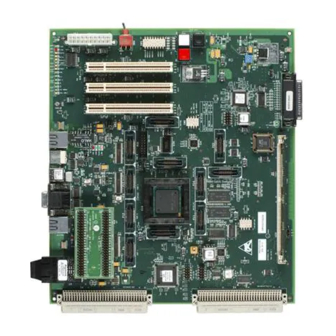
9" (229 mm) Thickness 0.063" (1.6 mm) MPC8272ADS Features This section summarizes the features of the MPC8272ADS. Major features are the following: • Supports MPC8272 (Hip7) processor • 64-bit PowerQUICC II Communication Processor, running at up to 100MHz external bus frequency •... - Page 21 • Separate power-on reset push button, soft / hard reset push button, and ABORT push button • ATX power supply • 1.3V to 1.7V (Hip7) internal logic operation voltage • Software option switch provides 8 S/W options using BCSR. Figure 1-1 shows the MPC8272ADS block diagram. Chapter 1. Overview...
- Page 22 DATA Transceivers & PROM Address Latches 8KByte 8 - bit SCC1 Reset, Main Interrupts Clock SCC4 3.3V 3.3V FCC2 Magnetics DM9161 3.3V Magnetics DM9161 FCC1 3.3V PM5384 PDIUSBP11 Logic Analyzer Buffered System Bus Mictors Figure 1-1. MPC8272ADS Block Diagram MPC8272ADS User Guide...
-
Page 23: Hardware Preparation And Installation
Hardware Preparation To ensure that the desired configuration is selected to produce proper operation of the MPC8272ADS board, changes of the dip-switch settings may be required before installation. The location of the switches, indicators, dip-switches, and connectors is illustrated in Figure 2-1. Boards are factory-tested and shipped with dip-switch settings as described in the following tested graphs. - Page 24 PC parallel port (P27). Selected automatically by connecting parallel cable. • Force PC parallel port (P27) connection using jumper JP12 • ATX power supply on/off switch using SW4 JP10 JP12 Figure 2-1. MPC8272ADS Top Side Part Location Diagram MPC8272ADS User Guide...
-
Page 25: Setting The Vddl Supply Voltage Level
Hardware Preparation 2.2.1 Setting the Supply Voltage Level VDDL The level of V is tuned using RP1 and is in the range of 1.3 V to 1.7 V. V may be measured upon JP13, using a DVM or any other high-input impedance voltage measuring device. -
Page 26: Setting Hard Reset Configuration Source-Jp9
Setting Hard Reset Configuration Source—JP9 The boot sequence that starts when HRESET is asserted can be from two sources: • BCSR (default hard-reset configuration word—CS0 is assumed to be assigned to the FLASH) • Memories (FLASH/EEPROM—user controlled hard-reset configuration word) MPC8272ADS User Guide... -
Page 27: Setting Boot Source
Hardware Preparation When a jumper is placed between positions 1–2 of JP9, the hard reset configuration source is a memory (FLASH/EEPROM) as configured by switch SW6-1. When a jumper is set between positions 2–3 of JP7, the hard reset configuration source is the BCSR. See Figure 2-4. -
Page 28: Setting Modckh(0:3) For Pll Multiplication Factors
When set high, the DLL is enabled. When switch SW6 #3 is at the OFF position, its corresponding PCI_DLL line is pulled-high (‘1’ - enabled). When at the ON position, pulled-down (‘0’ - disabled) (see Figure 2-5). MPC8272ADS User Guide... -
Page 29: Clock-In Source Selection
Hardware Preparation 2.2.8 Clock-In Source Selection The main clock source can be selected between an external (off-board) source by connecting to P6 or an on-board clock oscillator. The selection is done by setting JP1. When a jumper is placed between positions 1–2 of JP1, the external clock source is enabled. When a jumper is placed between positions 2–3 of JP1, the on-board clock oscillator is enabled (see Figure 2-6). -
Page 30: Fcc2 Ethernet Port Mode-Mii/Rmii
The USB port supports two modes, host and slave. The selection is done by setting JP8. When a jumper is placed between positions 1–2 of JP8, the slave mode is enabled. When a jumper is placed between positions 2–3 of JP8, the host mode is enabled (see Figure 2-9). MPC8272ADS User Guide... -
Page 31: Cop/Jtag Connection
Hardware Preparation Host Mode Slave Mode Factory Setup Figure 2-9. USB Mode Selection 2.2.13 COP/JTAG Connection Either of two options can establish connection to the COP port of the PowerQUICC II: COP/JTAG connector or a parallel port of a PC. The COP/JTAG connector requires a command converter, and the second option connects directly to the parallel port of a PC and eliminates the need for one. - Page 32 Hardware Preparation MPC8272ADS User Guide...
-
Page 33: Installation Instructions
Installation Instructions This chapter provides installation instructions for the MPC8272ADS. Installation Instructions When the MPC8272ADS has been configured as desired by the user, it can be installed according to the required working environment as follows: • Host-controlled operation • Stand-alone 3.1.1... -
Page 34: Stand Alone Operation
Ethernet port, ATM155 port, and so on. Operating in this mode requires programming an application program into the board’s Flash memory. Host Computer RS232 Ethernet ATM 155 (optics) ATX Power Supply P1A/P1B Figure 3-3. Stand Alone Configuration MPC8272ADS User Guide... -
Page 35: Cop/Jtag Connector-P21
The MPC8272ADS COP interface connector P21 is a 16-pin, male header connector. The connection between the MPC8272ADS and the COP controller is by a 16-line flat cable supplied with the COP controller board obtained from a third party developer. Figure 3-4 shows the pin configuration of the connector. -
Page 36: 10/100-Base-T Ethernet Ports Connection
A standard cable that has two RJ45/8 jacks on its ends connects the 10/100-Base-T ports to the network. The pinout of P10 and P23 is described in Table 8-2. 3.1.6 Memory Installation The MPC8272ADS is supplied with one type of memory module, the Flash memory SIMM. 3.1.6.1 Flash Memory SIMM Installation... -
Page 37: Operating Instructions
The ABORT switch ends program execution by issuing a level 0 interrupt to the MPC8272. If the ADS is in standalone mode, the user must provide a means for handling the interrupt, because the MPC8272ADS does not have a resident debugger. The ABORT switch signal is debounced and may be disabled by software. -
Page 38: Reset Configuration Switch-Sw2
If this process is done by unskilled hands or repeated more than 3 times, the MPC8272ADS can be permanently damaged. 4.1.8 Thermal Sense Connector—JP7 Two dedicated pins THERM(0:1) provide a way to take internal temperature measurements of the MPC8272. -
Page 39: Iddh Measurement-Jp14
If this process is done by unskilled hands or repeated more than 3 times, the MPC8272ADS can be permanently damaged. 4.1.10 V Source Selector—JP4 JP4 selects the source for V programming voltage for the Flash SIMM. -
Page 40: Power O.k. Indicator-Ld13
Controls and Indicators 4.1.11 GND Bridges The MPC8272ADS has seven GND bridges that are meant to assist general measurements and the logic-analyzer connection. Warning When connecting to a GND bridge, use only insulated GND clips. Un-insulated clips may cause short-circuits that touch hot points around them. -
Page 41: Run Indicator-Ld18
Controls and Indicators 4.1.19 RUN Indicator—LD18 When the green RUN led - LD18 is lit, it indicates that the MPC8272 is performing cycles on the PPC bus. When dark, the MPC8272 is either running internally or stuck. 4.1.20 ATM ON Indicator—LD19 When the yellow ATM ON led is lit, it indicates that the ATM-UNI transceiver PM5384 is enabled for communication. -
Page 42: Fast Ethernet Port 1 100Base-Tx Indicator-Ld2
When the DM9161 on FCC2 is enabled and is in 100 Mbps operation mode, the green led LD7 lights. 4.1.33 USB Enabled Indicator—LD21 The yellow USB enable LED indicates that the USB transceiver is connected to the MPC8272. MPC8272ADS User Guide... -
Page 43: Ethernet Port 2 Link Indicator-Ld9
Controls and Indicators 4.1.34 Ethernet Port 2 LINK Indicator—LD9 The yellow Ethernet twisted pair link integrity LED indicator (LINK) lights to indicate good link integrity on the 10/100-Base-T port. When the link integrity fails, LD9 is off. 4.1.35 Ethernet Port 2 Tx/Rx Indicator—LD8 The green Ethernet transmit/receive LED indicator blinks whenever the Dm9161 on FCC2 is transmitting or receiving data using the 10/100-Base-T port. - Page 44 Controls and Indicators MPC8272ADS User Guide...
-
Page 45: Module Design
This chapter provides information about the functionality and design details of the various modules that constitute the MPC8272ADS. Reset and Reset Configuration The following are reset sources on the MPC8272ADS: • Power-on reset • Manual hard reset • Manual soft reset •... -
Page 46: Hard Reset
PCI bus frequency by two. When reset low, the PCI bus frequency is as determined by the MODCK(1:3) and PCI_MODCKH(0:3) signals. 5.1.3 Hard Reset Hard reset may be generated on the MPC8272ADS by the following sources: • COP/JTAG port • Manual hard reset • MPC8272’s internal sources... -
Page 47: Manual Hard Reset
Because the HRESET line may be driven internally by the MPC8272, it must be driven to the MPC8272 with an open-drain gate. If off-board hardware connected to the MPC8272ADS is to drive HRESET line, it should do so with an open-drain gate, to avoid contention over this line. - Page 48 PROM or as default in the BCSR, while the other seven words are not initialized, as there are no additional MPC8272 on the MPC8272ADS. The default configuration word is shown in Table 5-1 for the FLASH and in Table 5-2 for the E PROM.
- Page 49 Reset and Reset Configuration Table 5-1. BCSR/FLASH Hard Reset Configuration Word (continued) Data Prog Offset In Value Field Value Implication Flash [Hex] Bits [Bin] [Hex] L2CPC ‘01’ CI/BADDR(29)/IRQ2 selected as IRQ2 WT/BADDR(30)/IRQ3 selected as IRQ3 L2_HIT/IRQ4 selected as IRQ4 CPU_BG/BADDR(31)/IRQ5 as IRQ5) DPPC 10:11 ‘11’...
- Page 50 Mask Masters Requests. Boot Master is 60x. LBPC 20:21 ’01’ Local Bus pins function as PCI bus. APPC 22:23 ’10’ MODCK1/AP(1)/TC(0) functions as BKSEL0 MODCK2/AP(2)/TC(1) functions as BKSEL1 MODCK3/AP(3)/TC(2) functions as BKSEL2 IRQ7~/APE~ functions as IRQ7~ CS11~/AP(0) functions as CS11~ MPC8272ADS User Guide...
-
Page 51: Soft Reset
Reset and Reset Configuration Table 5-2. E PROM Hard Reset Configuration Word (continued) Data Prog Offset In Value Field Value Implication Flash [Hex] Bits [Bin] [Hex] CS10PC 24:25 ’01’ CS10~/BCTL1/DBG_DIS~ functions as BCTL1 ALD_EN ’0’ PCI Auto Load Enable. When high, PCI Bridge Configuration is done automatically from the FLASH/E PROM (CPM is configuration source... -
Page 52: Cop/Jtag Port Soft Reset
Since the SRESET line may be driven internally by the MPC8272, it must be driven by an open-drain gate, to avoid contention over that line. If off-board H/W connected to the MPC8272ADS is to drive SRESET line, then, it should do so with an open-drain gate, this, to avoid contention over this line. -
Page 53: Local Interrupter
Reset and Reset Configuration 5.1.6 Local Interrupter The following external interrupts are applied to the MPC8272 using its interrupt controller: • ABORT (NMI) • ATM UNI interrupt • Fast Ethernet PHY interrupt • PCI interrupt 5.1.6.1 ABORT Interrupt The ABORT (NMI) is generated by a push-button. When this button is depressed, the IRQ0 input to the MPC8272 is asserted. - Page 54 ‘1’ - an interrupt was requested and waiting to be handled PCI0_INTD PCI Slot 0 INTD. PCI Slot 0 Interrupt D: ‘0’ - no interrupt was requested ‘1’ - an interrupt was requested and waiting to be handled MPC8272ADS User Guide...
- Page 55 Reset and Reset Configuration Table 5-3. PCI Interrupt Register Description (continued) MNEMONIC Function PCI1_INTA PCI Slot 1 INTA. PCI Slot 1 Interrupt A: ‘0’ - no interrupt was requested ‘1’ - an interrupt was requested and waiting to be handled PCI1_INTB PCI Slot 1 INTB.
- Page 56 Mask PCI Slot 2 INTC. Mask PCI Slot 2 Interrupt C: ‘0’ - interrupt is available ‘1’ - interrupt is masked Mask PCI Slot 2 INTD. Mask PCI Slot 2 Interrupt D: MPCI2_INTD ‘0’ - interrupt is available ‘1’ - interrupt is masked 12-31 Reserved Un-implemented MPC8272ADS User Guide...
-
Page 57: Clock Generator
Clock Generator Clock Generator The two main clock circuits on board are the following: • MPC8272 system clock • PCI clock 5.2.1 MPC8272 Clock The MPC8272 requires a single clock source as the main clock source. All MPC8272 60x bus timings are referenced to the main clock input - CLKIN1. The main clock input is in 1:1 ratio to the bus clock, with internal skew elimination (PLL). -
Page 58: Bus Configuration
Required for Flash, E PROM, Interrupt Controller and BCSR An address which is covered in a Chip-Select region, that controls a buffered device. To allow a configuration word stored in the Flash/E PROM memory to become active. MPC8272ADS User Guide... -
Page 59: Chip-Select Generator
The MPC8272 chip-select assignments to the various memories / registers on the MPC8272ADS are shown in Table 5-5. Table 5-5. MPC8272ADS Chip Select Assignments Chip Select: Assignment... -
Page 60: Sdram Programming
SDRAM’s address lines. This command is fully supported by the SDRAM machine of the MPC8272. Before that can occur, the SDRAM machine of the MPC8272 must be initialized. MPC8272ADS User Guide... -
Page 61: Sdram Refresh
Flash SIMM inserted to the MPC8272ADS. The access time of the Flash memory provided with the MPC8272ADS is 95 nsec. However, devices with different delay are supported as well. By reading the delay section... - Page 62 ’1’ /’0’ respectively to the FlashEn bit in BCSR1. The Flash connection scheme is shown in Figure 5-6. FLASH SIMM DATA(0:31) D(31:0) ADDRESS(7:29) A(22:0) BCSR FLASH Figure 5-6. FLASH SIMM Connection Scheme i.e., initialization that follow the hard reset sequence at system boot. MPC8272ADS User Guide...
-
Page 63: Flash Programming Voltage
Flash, Motorola recommends leaving the jumper open so that no V applied to the Flash SIMM. PROM Memory The MPC8272ADS is provided with 8KBytes of E PROM memory in a PLCC package. The E PROM resides on a socket in case it is desired to replace or re-program a different configuration for the board. -
Page 64: Pci Bus
The MPC8272 also includes an on-chip arbiter which enables arbitration of up to three PCI masters. Only three PCI slots are supported on the MPC8272ADS because of the Arbiter capacity. Each slot can host either a PCI master or PCI target. The MPC8272 as a Bridge can support more PCI devices but that will require extra slots that can host PCI targets only. - Page 65 25MHz up to 66MHz @ 3.3V only. The 3.3V restriction is due to the MPC8272 which is not 5V compliant. The PCI bus layout is shown in Figure 5-8 Special care was taken when the layout of the MPC8272ADS was done so that the PCI standard recommendations are followed strictly.
-
Page 66: Communication Ports
Communication Ports 5.10 Communication Ports The MPC8272ADS has several communication ports, to allow convenient evaluation of the CPM features. Obviously, it is not possible to provide all types of communication interfaces supported by the CPM, but it is made convenient to connect any communication interface devices to the MPC8272 via the CPM Expansion connectors, residing on the edge of the board. -
Page 67: 100/10 Base T Ports
- devices’ control and data path. The initial configuration of the DM9161 on the MPC8272ADS is set by external resistors - 100Base-Tx Full Duplex in MII mode. The selection between MII/RMII for FCC1 and FCC2 is done by jumpers JP5 and JP10 respectively. -
Page 68: Rs232 Ports
Figure 5-9. RS232 Serial Ports Connector 5.10.3.1 RS-232 Ports’ Signal Description In the list below, the directions ’I’,’O’, and ’I/O’ are relative to the MPC8272ADS board. (i.e.’I’ means input to the MPC8272ADS) • CD (O) - Data Carrier Detect. This line is always asserted by the MPC8272ADS. -
Page 69: Usb Port
• 5.10.4 USB Port The USB port resides on the MPC8272ADS and is driven by the USB port of the MPC8272 through SCC3. A dedicated USB transceiver - the PDIUSBP11 by PHILIPS is provided, along with a tri-state buffer, separating this port from the MPC8272’s USB port, this to allow Port disable option and off-board use of MPC8272 USB pins. - Page 70 Since part of the MPC8272ADSs’ modules are controlled by the BCSR and since they may be disabled in favor of external hardware, the enable signals for these modules are presented at the CPM expansion connectors, so that off- board hardware may be mutually exclusive enabled with on-board modules. MPC8272ADS User Guide...
-
Page 71: Bcsr0 Board Control-Status Register 0
Board Control and Status Register - BCSR 5.11.1 BCSR0 Board Control—Status Register 0 The BCSR0 is a control register on the MPC8272ADS. It is accessed at offset 0 from BCSR base address. It may be read or written at any time . -
Page 72: Bcsr2 Board Control-Status Register 2
These signals are available at the System expansion connector. The revision option for the external tools are shown in Table 5-15 Provided that BCSR is not disabled. MPC8272ADS User Guide... - Page 73 Un-implemented 20 - 21 BVERN(0:1) Board Version Number (0:1). This field represents the version code, hard-assigned to the MPC8272ADS. See Table 5-13, for version encoding. 22 - 23 BREVN(0:1) Board Revision Number (0:1). This field represents the revision code, hard-assigned to the MPC8272ADS. See Table 5-14, for revisions’...
- Page 74 Table 5-13. PowerQUICC II Board Version Encoding Version Number (0:1) [Hex] PowerQUICC II Board Version PowerQUICC IIFADS-ZU Reserved MPC8272ADS PowerQUICC II7e ADS Table 5-14. PowerQUICC II Board Revision Encoding Revision Number (0:1) [Hex] PowerQUICC II Board Revision ENG (Engineering) PILOT Reserved MPC8272ADS User Guide...
-
Page 75: Bcsr3 Board Control - Status Register 3
Board Control and Status Register - BCSR Table 5-15. External Tool Revision Encoding TOOLREV(0:3) [hex] External Tool Revision ENGINEERING PILOT 3 - F Reserved 5.11.4 BCSR3 Board Control - Status Register 3 BCSR3 is a control register which is accessed at offset 0xC from the BCSR base address. Its a read- write register which may be read or written at any time . -
Page 76: Bcsr4 Board Control-Status Register 4
PCI_MODCK. This field shows the PCI bus clock settings. 8-31 Reserved un-implemented Table 5-18. PCI Board Present Signal Definitions PCIx_PRSNT (0:1) [Hex] Expansion Configuration Expansion board present, 7.5W maximum Expansion board present, 25W maximum Provided that BCSR is not disabled. MPC8272ADS User Guide... -
Page 77: Bcsr5 And Bcsr7 Board Control-Status Register 3 And 5
Figure 5-10. Debug Station Connection Schemes To support debug station connection to the COP/JTAG port, a 16 pin generic header connector is provided on the MPC8272ADS, carrying the COP/JTAG signals as well as Not provided with the MPC8272ADS. Chapter 5. Module Design... - Page 78 PowerQUICC II. TRST Test port Reset (L). When this signal is active (Low), it resets the JTAG logic. This line is pull-down on the MPC8272ADS with a 1KΩ resistor, to provide constant reset of the JTAG logic. QREQ Quiescent Request (L).
- Page 79 This line may be driven by the PowerQUICC II as well during soft-reset sequence, for 512 system clocks. This line is pulled up on the MPC8272ADS with a 1KΩ resistor. When driven externally, it MUST be driven with an Open Drain gate.
- Page 80 COP/JTAG Port MPC8272ADS User Guide...
-
Page 81: Memory Map
This chapter explains memory mapping in the MPC8272ADS. Overview All accesses to MPC8272ADS memory slaves are controlled by the MPC8272 memory controller. Therefore, the memory map is reprogrammable to suit the user. After the debug station performs hard reset, the debugger checks for existence, size, delay and type of the Flash memory SIMM mounted on board, decides the assignments of CS0 and CS4 PROM and Flash), and programs the memory controller accordingly. - Page 82 Overview — Table 6-1. MPC8272ADS Memory Map Flash (or BCSR) as Boot Device Address Memory Port Memory Device Name Range Type Size Size 04500000 - BCSR(0:7) 32 KBytes 04507FFF 04500000 - BCSR0 4 Bytes 04507FE3 04500004 - BCSR1 4 Bytes...
- Page 83 Overview — Table 6-1. MPC8272ADS Memory Map Flash (or BCSR) as Boot Device Address Memory Port Memory Device Name Range Type Size Size C0000000 - Empty space 32 MBytes C1FFFFFF C2000000 PROM ATMEL AT28HC64B 32 KBytes C2007FFF C2008000 - Empty space...
- Page 84 Overview — Table 6-2. MPC8272ADS Memory Map PROM as Boot Device Address Memory Port Memory Device Name Range Type Size Size 04500000 - 32 KBytes BCSR(0:7) 04507FFF 4 Bytes 04500000 BCSR0 04507FE3 4 Bytes 04500004 BCSR1 04507FE7 04500008 BCSR2 4 Bytes...
-
Page 85: Powerquicc Ii Register Programming
An 8-Kbyte device is used (16- and 32-Kbyte devices can also be used) so it appears repeatedly in 8 Kbyte multiples starting from FFF00000. PowerQUICC II Register Programming The PowerQUICC II provides the following functions on the MPC8272ADS: • System functions that include the following: — PPC bus SDRAM controller —... -
Page 86: System Initialization
Boot memory space @ 0xFE000000 - 0xFFFFFFFF, ABB/IRQ2 pin is ABB, DBB/IRQ3 pin is DBB, No masking on bus request lines, Local bus pins function as PCI, PCI is boot master, AP(1;3) configured as BNKSEL(0:2), APE configured as IRQ7 and CS11 as CS11. CS10 configured as BCTL1 MPC8272ADS User Guide... -
Page 87: Memory Controller Register Programming
6.2.2 Memory Controller Register Programming The memory controller on the MPC8272ADS is initialized to 100MHz operation, that is, the registers’ programming is based on 100-MHz timing calculation. It also works for slower bus speeds, but the timing must be optimized). The two possible initialization for the memory controller are the following: •... - Page 88 00000041 Base at 0, 64 bit port size, no parity, SDRAM MT48LC8M16A2 machine 1 MICRON FE002EC0 32MByte block size, 4 banks per device, row starts at A7, 12 row lines, internal bank interleaving allowed, normal AACK operation MPC8272ADS User Guide...
- Page 89 PowerQUICC II Register Programming Table 6-7. Memory Controller Initialization For 100MHz—E PROM as Boot Device Init Value Reg. Device Type Description [hex] SM73228XG1JHBG0 by C3801801 Base at C3800000, 32 bit port size, no parity, Smart Modular Tech. GPCM SM73248XG2JHBG0 by C3001801 Base at C3000000, 32 bit port size, no parity, Smart Modular Tech.
- Page 90 PowerQUICC II Register Programming MPC8272ADS User Guide...
-
Page 91: Physical Properties
(I/O) • V (Internal Logic) • VCCSYN (CPM PLL) • VCCSYN1 (core PLL) The MPC8272ADS (see Figure 7-1) has the following power rails on it: • VCC (5V) rail • Stand By (5V) rail • V3.3 (3.3V) rail • V (1.7V-2.5V) rail... - Page 92 VDDH Power Supply PowerQUICC II Figure 7-1. MPC8272ADS Power Scheme To support off-board application development, the power buses are connected to the expansion connectors so that external logic may be powered directly from the board. The maximum current allowed to be drawn from the board on each bus also depends on the current drawn by the PCI bus.
-
Page 93: 5-V Rail
7.1.1 5-V Rail Some of the MPC8272ADS peripherals (not including the PCI add-in cards that should be 3.3 V only on the PCI interface, but can use 5 V for other components on-board) reside on the 5-V bus. Because the MPC8272 is not 5-V tolerant, buffering is provided between 5V peripherals and the MPC8272, protecting the MPC8272 from the higher voltage level. -
Page 94: 12-V Rail
PCB and the plug is connected to the power supply to facilitate fast connection or disconnection of power. 7.2.2 Fast Ethernet Port Connectors The Ethernet connector on the MPC8272ADS is a twisted-pair (100/10-Base-T) connector. Use is done with 90 RJ45-8 connector. MPC8272ADS User Guide... -
Page 95: Atm 155 Port Connection
Connectors 7.2.3 ATM 155 Port Connection The ATM 155 I/F to the media is optical rather than electrical. Use is done with HP’s HFBR 5805 optical I/F, which is placed on the edge of the board for convenient connection. 7.2.4 RS232 Port Connector The RS232 port connector is a stacked 9-pin, 90 , female D-Type connector that saves board... -
Page 96: System Expansion Connector
The parallel connector is a standard 25 pin D-Type male connector. PCB Layout The MPC8272ADS layout was done for high-frequency operation and follows the PCI standard layout recommendations closely. The following list of measures are taken to meet this design goal: •... -
Page 97: Interconnect Signals
Support This chapter provides all information needed for support, maintenance and connectivity to the MPC8272ADS. Interconnect Signals The MPC8272ADS interconnects with external devices by using the following set of connectors: 1. P13—RS232 ports 1 and 2 2. P16, P19—USB connectors 3. -
Page 98: P10 And P23 100/10 Base-T Ethernet Port Connector
Table 8-2. P10,P23 100/10 Base-T Ethernet Connector Pin No. Signal Name Description TPTX Twisted-pair transmit data positive output from the MPC8272ADS TPTX~ Twisted-pair transmit data negative output from the MPC8272ADS TPRX Twisted-pair receive data positive input to the MPC8272ADS N.C. - Page 99 Interconnect Signals Table 8-3. P16—COP/JTAG Connector (continued) Pin No. Signal Name Attribute Description TRST# Test port reset~ (L). When this signal is active (Low), it resets the JTAG logic of the PowerQUICC II. This line is pull-down on the ADS with a 1KΩ resistor, to provide constant reset of the JTAG logic.
-
Page 100: P1-Cpm Expansion Connector
ATM Multi-PHY Tx Address 4. When the ATM port Multi-PHY function is enabled, this line is connected to the transmit PHY Address of the PM5384 ATM UNI. When this port is disabled, this signal is tristated and may be used for any available function of PD19. MPC8272ADS User Guide... - Page 101 Interconnect Signals Table 8-4. P1—CPM Expansion Connector (continued) Pin No. Signal Name Attribute Description ATMRXADR4(PD18) I/O, T.S ATM Multi-PHY Rx Address 4. When the ATM port Multi-PHY function is enabled, this line is connected to the receive PHY Address of the PM5384 ATM UNI. When this port is disabled, this signal is tristated and may be used for any available function of PD18.
- Page 102 When the port is operation at 100 Mbps, the DM9161 responds by sending invalid code symbols on the line. When the Ethernet port is disabled, this line may be used for any available function of PA29. MPC8272ADS User Guide...
- Page 103 Interconnect Signals Table 8-4. P1—CPM Expansion Connector (continued) Pin No. Signal Name Attribute Description ATMRXEN# (PA28) I/O, T.S. ATM Receive Enable (L). When this signal is asserted (Low), while the ATM port is enabled and ATMRFCLK goes high, on octet of data is available at the PM5384’s ATMRXD(7:0) lines.
- Page 104 FETH1RXD2 (PA15) ATMRXD4 (PA14) FETH1RXD3 (PA14) ATMRXD3 (PA13) ATMRXD2 (PA12) ATMRXD1 (PA11) ATMRXD0 (PA10) I/O, T.S. PowerQUICC II’s Port A (9:0). Parallel I/O or dedicated CPM lines. May be used for any of their available functions. PC27 MPC8272ADS User Guide...
- Page 105 Interconnect Signals Table 8-4. P1—CPM Expansion Connector (continued) Pin No. Signal Name Attribute Description PC26 PB27 PB26 PB25 PB24 RS_RXD2 (PD22) I/O, T.S. When RS232 port #2 is enabled, this signal is the receive data line for that port. When this port is disabled, this signal is tristated and may be used to any available alternate function for PD22.
- Page 106 Otherwise, Tri-stated. Digital Ground. Connected to main GND plane of the ADS. PC31 PowerQUICC II’s Port C (31:22) Parallel I/O lines. May be used to I/O, T.S. any of their available functions. PC30 PC29 PC28 MPC8272ADS User Guide...
- Page 107 Interconnect Signals Table 8-4. P1—CPM Expansion Connector (continued) Pin No. Signal Name Attribute Description PC25 USBCLK USB Clock Line. When the USB port is enabled, this line is connected to the USB clock line. When this port is disabled, this signal is tristated and may be used for any available function of PC24.
- Page 108 RS232 DTR2# input, allowing detection of a connected terminal to this port. This line is simply a PI/O input line to the PowerQUICC When RS232 Port 2 is disabled, this line is tristated and may be used for any available function of PC8. MPC8272ADS User Guide...
-
Page 109: Logic Analyzer Mictor Connectors
Interconnect Signals Table 8-4. P1—CPM Expansion Connector (continued) Pin No. Signal Name Attribute Description The functions in parenthesis, are PowerQUICC II’s parallel I/Os. For that matter, both 100-Base-T and 10-Base-T. Normally connected to ATMTFCLK on the ADS. MS bit. For that matter, both 100-Base-T and 10-Base-T. 8.1.5 P9, P11, P14, P22, P17, P5, P20, P18, P15, P24,P12 Logic Analyzer MICTOR Connectors... - Page 110 Ground +3.3V AD[24] C/BE[3]# IDSEL AD[23] +3.3V Ground AD[22] AD[21] AD[20] AD[19] Ground +3.3V AD[18] AD[17] AD[16] C/BE[2]# +3.3V Ground FRAME# IRDY# Ground +3.3V TRDY# DEVSEL# Ground Ground STOP# LOCK# Not Connected +3.3V PERR# SDONE Not Connected MPC8272ADS User Guide...
-
Page 111: P31 - Atx Power Supply Connector
Interconnect Signals — Table 8-5. P26, P28, P29 PCI Connectors (continued) Side B Comments Side A Comments Number +3.3V SBO# Not Connected SERR# Ground +3.3V C/BE[1]# AD[15] AD[14] +3.3V Ground AD[13] AD[12] AD[11] AD[10] Ground M66EN Coupled to GND, AD[09] using a 0.01uF capacitor Ground... -
Page 112: P3,P4,P25-Mach/Lattice Isp Connector
TCK. 5V power supply bus. ISPTDO ISP transmit data output. This the prog. logic’s JTAG serial data output driven by falling edge of TCK. Digital GND. Main GND plane. N.C. Not connected N.C. Not connected MPC8272ADS User Guide... -
Page 113: P2-System Expansion Connector
Interconnect Signals 8.1.9 P2—System Expansion Connector P2 is a 128-pin, 90 , DIN 41612 connector that provides a minimal system I/F required to interface various types of communication transceivers. This connector contains 16-bit (lower PPC bus) address lines, 16-bit (higher PPC bus) data lines, plus useful GPCM and UPM control lines. - Page 114 KΩ resistors. See also Table 10-38. "BCSR2 Description" on page EXTOLI2 EXTOLI3 N.C. Not connected EXP3.3V 3.3V Power Out. These lines are connected to the main 3.3V plane of the PowerQUICC IIPCIAI-ADS, this, to provide 3.3V power where necessary for external tool connected. MPC8272ADS User Guide...
- Page 115 Interconnect Signals — Table 8-8. P2 System Expansion Connector (continued) Pin No. Signal Name Attribute Description N.C. Not Connected EXPVCC 5V Supply. Connected to ADS’s 5V VCC plane. Provided as power supply for external tool. Digital Ground. Connected to main GND plane of the ADS. CLK8 Buffered System Clock..
- Page 116 The direction of these lines is determined by buffered BCTL0, in function of W/R#. EXPD3 EXPD4 EXPD5 EXPD6 EXPD7 EXPD8 EXPD9 EXPD10 EXPD11 EXPD12 EXPD13 EXPD14 EXPD15 N.C. Not connected Digital ground. Connected to main GND plane of the ADS. MPC8272ADS User Guide...
- Page 117 Interconnect Signals — Table 8-8. P2 System Expansion Connector (continued) Pin No. Signal Name Attribute Description EXPWE0# Expansion Write Enable (0:1) (L). These are buffered GPCM Write Enable lines (0:1). They are meant to qualify writes to GPCM EXPWE1# controlled 8/16 data bus width memory devices. This to provide eased access to various communication transceivers.
-
Page 118: P16, P19-Usb Connectors
These are four pins standard USB connectors type-A and Type-B. The pinout is shown in Table 8-9. — Table 8-9. P16, P19 USB Connectors Pin No. Signal Name Description 5V Power Power line of the USB cable Twisted-pair transmit data negative Twisted-pair receive data positive Ground connection MPC8272ADS User Guide... -
Page 119: Programmable Logic Equations
1. U3 - BCSR and PCI interrupt controller 2. U5 - Power switch debounce 8.2.1 U3—BCSR Code MODULE MPC8272ADS_BCSR TITLE 'MPC8272ADS control status register' "****************************************************************************** "* This file (Prototype) is based on the PQ2FADS-VR (08/21/03): "****************************************************************************** "****************************************************************************** "* In this file (Prototype) the following changes were made (03/06/03): "* - Adjustments for VR board were done - PCI only support in config Word (LBPC). - Page 120 FEth1PLLOn_B PIN 131 ; " FEth1 TxCLK clock buffer PLL On for 100Base-T MII1PLLOff_B PIN 129istype'com' ; " FEth1 TxCLK buffer PLL Off - 10Base-T FEth2PLLOn_B PIN 127 ; " FEth2 TxCLK clock buffer PLL On for 100Base-T MPC8272ADS User Guide...
- Page 121 Programmable Logic Equations MII2PLLOff_B PIN 117istype'com' ; " FEth2 TxCLK buffer PLL Off - 10Base-T RS232En1_B 32istype 'reg,buffer' ; " RS232 port 1 enable RS232Dis1_B 56istype 'com' ; " RS232 port 1 Disable RS232En2_B 3istype 'reg,buffer' ; " RS232 port 2 enable RS232Dis2_B 8istype 'com' ;...
- Page 122 HardResetEnNODE istype 'com' ; " enables T.S. hard reset pin SoftResetEnNODE istype 'com' ; " enables T.S. soft reset pin "****************************************************************************** "* data buffers enable. "****************************************************************************** SyncHardReset_B NODE istype 'reg,buffer' ; " synchronized hard reset DSyncHardReset_B NODE istype 'reg,buffer' ; " double synchronized hard reset HoldOffCnt2, MPC8272ADS User Guide...
- Page 123 Programmable Logic Equations HoldOffCnt1, HoldOffCnt0 NODE istype 'reg,buffer' ; " data buf en hold-off counter HoldOffTc NODE istype 'com' ; " terminal count for that counter "****************************************************************************** "* Power On Reset "****************************************************************************** S_PORIn_B NODE istype 'reg,buffer' ; " synced pon reset. "****************************************************************************** "* PCI Interrupt Register.
- Page 124 AtmRst_B, AtmSinglePHY_B, FEthEn1_B, FEthRst1_B, FEthEn2_B, FEthRst2_B, RS232En1_B, RS232En2_B, USBEn_B, USBHiSpd_B, USBVccO] ; ReadBcsr0 = [0, SignaLamp0_B, SignaLamp1_B] ; ReadBcsr1 = [bcsrConfEn, boot_device_B, AtmEn_B, AtmRst_B.fb, FEthEn1_B, FEthRst1_B.fb, RS232En1_B, RS232En2_B] ; ReadBcsr3 = [USBEn_B, USBHiSpd_B, USBVccO, FEthEn2_B, FEthRst2_B.fb, AtmSinglePHY_B, MPC8272ADS User Guide...
- Page 125 Programmable Logic Equations PCI_Mode_B]; DrivenContReg = [SignaLamp0_B, SignaLamp1_B, AtmEn_B, AtmSinglePHY_B, FEthEn1_B, FEthEn2_B, RS232En1_B, RS232En2_B, USBEn_B] ; " USBVccO] ; ClockedContReg = [SignaLamp0_B, SignaLamp1_B, AtmEn_B, AtmRst_B, AtmSinglePHY_B, FEthEn1_B, FEthEn2_B, FEthRst1_B, FEthRst2_B, RS232En1_B, RS232En2_B, USBEn_B, USBHiSpd_B, USBVccO] ; IntReg = [Slot0IntA, Slot0IntB, Slot0IntC, Slot0IntD, Slot1IntA,...
- Page 126 VGR_READ_BCSR_4 = (!BrdContRegCs_B & !R_B_W & A27 & !A28 & !A29) ; "****************************************************************************** "****************************************************************************** "* BCSR 0 definitions. "****************************************************************************** "****************************************************************************** SIGNAL_LAMP_ON = 0 ; "*********************************************** "******* Power On Defaults Assignments "*********************************************** SIGNAL_LAMP0_PON_DEFAULT = !SIGNAL_LAMP_ON ; SIGNAL_LAMP1_PON_DEFAULT = !SIGNAL_LAMP_ON ; MPC8272ADS User Guide...
- Page 127 Programmable Logic Equations "******************************************* "******* Data Bits Assignments "******************************************* SIGNAL_LAMP0_DATA_BIT = [D6] ; SIGNAL_LAMP1_DATA_BIT = [D7] ; "****************************************************************************** "****************************************************************************** "* BCSR 1 definitions. "****************************************************************************** "****************************************************************************** BCSR_BOOT = 0 ;" bcsrConfEn = 0 Hard Reset Conf Word from BCSR MEMORY_BOOT = 1 ;" bcsrConfEn = 1 Hard Reset Conf from EEPROM/FLASH FLASH_BOOT = 0 ;"...
- Page 128 "* PCI Interrupt Register definitions. "****************************************************************************** "****************************************************************************** Slot0IntA_Active = 1 ; " PCI Slot 0 Interrupt A asserted Slot0IntB_Active = 1 ; " PCI Slot 0 Interrupt B asserted Slot0IntC_Active = 1 ; " PCI Slot 0 Interrupt C asserted MPC8272ADS User Guide...
- Page 129 Programmable Logic Equations Slot0IntD_Active = 1 ; " PCI Slot 0 Interrupt D asserted Slot1IntA_Active = 1 ; " PCI Slot 1 Interrupt A asserted Slot1IntB_Active = 1 ; " PCI Slot 1 Interrupt B asserted Slot1IntC_Active = 1 ; " PCI Slot 1 Interrupt C asserted Slot1IntD_Active = 1 ;...
- Page 130 (SM73288XU4 & !A7 & !A8) ) ; FLASH_BANK2 = ( (SM73248XU2 & A8) # (SM73288XU4 & !A7 & A8) ) ; FLASH_BANK3 = ( A7 & !A8 & SM73288XU4 ) ; FLASH_BANK4 = ( A7 & A8 & SM73288XU4 ) ; "****************************************************************************** MPC8272ADS User Guide...
- Page 131 Programmable Logic Equations "* ATM UNI Declarations. "****************************************************************************** "****************************************************************************** "* Reset Declarations. "****************************************************************************** HARD_RESET_ACTIVE = 0 ; SOFT_RESET_ACTIVE = 0 ; HARD_RESET_ASSERTED = (SyncHardReset_B.fb == HARD_RESET_ACTIVE) ; "****************************************************************************** "* data buffers enable. "****************************************************************************** BUFFER_DISABLED = 1 ; BUFFER_ENABLED = !BUFFER_DISABLED ; BUFFER_HOLD_OFF = (HoldOffCnt.fb != 0) ;...
- Page 132 (!PON_RESET # (SIGNAL_LAMP1_PON_DEFAULT != SIGNAL_LAMP_ON)) # (PON_RESET & (SIGNAL_LAMP1_PON_DEFAULT == !SIGNAL_LAMP_ON)) ) then !SIGNAL_LAMP_ON else SIGNAL_LAMP_ON ; state !SIGNAL_LAMP_ON: if (VGR_WRITE_BCSR_0 & (SIGNAL_LAMP1_DATA_BIT.pin == SIGNAL_LAMP_ON) & (!PON_RESET # (SIGNAL_LAMP1_PON_DEFAULT != !SIGNAL_LAMP_ON)) # (PON_RESET & (SIGNAL_LAMP1_PON_DEFAULT == SIGNAL_LAMP_ON)) ) then MPC8272ADS User Guide...
- Page 133 Programmable Logic Equations SIGNAL_LAMP_ON else !SIGNAL_LAMP_ON ; "****************************************************************************** "****************************************************************************** "* BCSR1 State Machines "****************************************************************************** "****************************************************************************** state_diagram AtmEn_B state ATM_ENABLED: if (VGR_WRITE_BCSR_1 & (ATM_ENABLE_DATA_BIT.pin == !ATM_ENABLED) & (!PON_RESET # (ATM_ENABLE_PON_DEFAULT != ATM_ENABLED)) # (PON_RESET & (ATM_ENABLE_PON_DEFAULT == !ATM_ENABLED)) ) then !ATM_ENABLED else ATM_ENABLED ;...
- Page 134 (PON_RESET & (RS232_2_ENABLE_PON_DEFAULT == !RS232_2_ENABLE)) ) then !RS232_2_ENABLE else RS232_2_ENABLE ; state !RS232_2_ENABLE: if (VGR_WRITE_BCSR_1 & (RS232_2_ENABLE_DATA_BIT.pin == RS232_2_ENABLE) & (!PON_RESET # (RS232_2_ENABLE_PON_DEFAULT != !RS232_2_ENABLE)) # (PON_RESET & (RS232_2_ENABLE_PON_DEFAULT == RS232_2_ENABLE)) ) then RS232_2_ENABLE else !RS232_2_ENABLE ; "****************************************************************************** "****************************************************************************** "* BCSR3 State Machines MPC8272ADS User Guide...
- Page 135 Programmable Logic Equations "****************************************************************************** "****************************************************************************** state_diagram USBEn_B state USB_ENABLED: if (VGR_WRITE_BCSR_3 & (USB_ENABLE_DATA_BIT.pin == !USB_ENABLED) & (!PON_RESET # (USB_ENABLE_PON_DEFAULT != USB_ENABLED)) # (PON_RESET & (USB_ENABLE_PON_DEFAULT == !USB_ENABLED)) ) then !USB_ENABLED else USB_ENABLED ; state !USB_ENABLED: if (VGR_WRITE_BCSR_3 & (USB_ENABLE_DATA_BIT.pin == USB_ENABLED) & (!PON_RESET # (USB_ENABLE_PON_DEFAULT != !USB_ENABLED)) # (PON_RESET &...
- Page 136 & (ATM_SINGLE_PHY_ENABLE_PON_DEFAULT == !ATM_SINGLE_PHY_ENABLED)) ) then !ATM_SINGLE_PHY_ENABLED else ATM_SINGLE_PHY_ENABLED ; state !ATM_SINGLE_PHY_ENABLED: if (VGR_WRITE_BCSR_3 & (ATM_SINGLE_PHY_ENABLE_DATA_BIT.pin == ATM_SINGLE_PHY_ENABLED) & (!PON_RESET # (ATM_SINGLE_PHY_ENABLE_PON_DEFAULT != !ATM_SINGLE_PHY_ENABLED)) # (PON_RESET & (ATM_SINGLE_PHY_ENABLE_PON_DEFAULT == ATM_SINGLE_PHY_ENABLED)) ) then ATM_SINGLE_PHY_ENABLED else !ATM_SINGLE_PHY_ENABLED ; "****************************************************************************** equations AtmMultiPHY_B = !AtmSinglePHY_B ; MPC8272ADS User Guide...
- Page 137 Programmable Logic Equations USBDis_B = !USBEn_B ; USBLowSpd_B = !USBHiSpd_B ; USBVccOut = !USBVccO ; FEthDis1_B = !FEthEn1_B ; FEthDis2_B = !FEthEn2_B ; RS232Dis1_B = !RS232En1_B ; RS232Dis2_B = !RS232En2_B ; FCC1On_B = FEthEn1_B & AtmEn_B ; FCC1Off_B = !FCC1On_B ; MIIOn_B = FEthEn1_B &...
- Page 138 (!(HardReset_B == 0) & ((PCI_INTD_B & !Slot1IntAMask.fb) # Slot1IntAMask.fb)) ) then !Slot1IntA_Active else Slot1IntA_Active ; state !Slot1IntA_Active: if ( ((HardReset_B == 0) & (Slot1IntA_PON_DEFAULT == Slot1IntA_Active)) # (!(HardReset_B == 0) & !PCI_INTD_B & !Slot1IntAMask.fb) ) then Slot1IntA_Active MPC8272ADS User Guide...
- Page 139 Programmable Logic Equations else !Slot1IntA_Active ; "****************************************************************************** state_diagram Slot1IntB state Slot1IntB_Active: if ( ((HardReset_B == 0) & (Slot1IntB_PON_DEFAULT == !Slot1IntB_Active)) # (!(HardReset_B == 0) & ((PCI_INTA_B & !Slot1IntBMask.fb) # Slot1IntBMask.fb)) ) then !Slot1IntB_Active else Slot1IntB_Active ; state !Slot1IntB_Active: if ( ((HardReset_B == 0) & (Slot1IntB_PON_DEFAULT == Slot1IntB_Active)) # (!(HardReset_B == 0) &...
- Page 140 ( ((HardReset_B == 0) & (Slot2IntD_PON_DEFAULT == !Slot2IntD_Active)) # (!(HardReset_B == 0) & ((PCI_INTB_B & !Slot2IntDMask.fb) # Slot2IntDMask.fb)) ) then !Slot2IntD_Active else Slot2IntD_Active ; state !Slot2IntD_Active: if ( ((HardReset_B == 0) & (Slot2IntD_PON_DEFAULT == Slot2IntD_Active)) # (!(HardReset_B == 0) & !PCI_INTB_B & !Slot2IntDMask.fb) ) then MPC8272ADS User Guide...
- Page 141 Programmable Logic Equations Slot2IntD_Active else !Slot2IntD_Active ; "****************************************************************************** "****************************************************************************** "* PCI Interrupt Mask Register "****************************************************************************** "****************************************************************************** equations IntMaskReg.clk = SYSCLK ; IntMaskReg.ar = 0 ; IntMaskReg.ap = 0 ; "****************************************************************************** state_diagram Slot0IntAMask state Slot0IntAMask_Active: if (VGR_WRITE_IntMaskReg & (Slot0IntAMask_DATA_BIT.pin == !Slot0IntAMask_Active) & (!(HardReset_B == 0) # (Slot0IntAMask_PON_DEFAULT == !Slot0IntAMask_Active)) # ((HardReset_B == 0) &...
- Page 142 !Slot1IntAMask_Active: if (VGR_WRITE_IntMaskReg & (Slot1IntAMask_DATA_BIT.pin == Slot1IntAMask_Active) & (!(HardReset_B == 0) # (Slot1IntAMask_PON_DEFAULT == Slot1IntAMask_Active)) # ((HardReset_B == 0) & (Slot1IntAMask_PON_DEFAULT == Slot1IntAMask_Active)) ) then Slot1IntAMask_Active else !Slot1IntAMask_Active ; "****************************************************************************** state_diagram Slot1IntBMask state Slot1IntBMask_Active: if (VGR_WRITE_IntMaskReg & MPC8272ADS User Guide...
- Page 143 Programmable Logic Equations (Slot1IntBMask_DATA_BIT.pin == !Slot1IntBMask_Active) & (!(HardReset_B == 0) # (Slot1IntBMask_PON_DEFAULT == !Slot1IntBMask_Active)) # ((HardReset_B == 0) & (Slot1IntBMask_PON_DEFAULT == !Slot1IntBMask_Active)) ) then !Slot1IntBMask_Active else Slot1IntBMask_Active ; state !Slot1IntBMask_Active: if (VGR_WRITE_IntMaskReg & (Slot1IntBMask_DATA_BIT.pin == Slot1IntBMask_Active) & (!(HardReset_B == 0) # (Slot1IntBMask_PON_DEFAULT == Slot1IntBMask_Active)) # ((HardReset_B == 0) &...
- Page 144 !Slot2IntCMask_Active else Slot2IntCMask_Active ; state !Slot2IntCMask_Active: if (VGR_WRITE_IntMaskReg & (Slot2IntCMask_DATA_BIT.pin == Slot2IntCMask_Active) & (!(HardReset_B == 0) # (Slot2IntCMask_PON_DEFAULT == Slot2IntCMask_Active)) # ((HardReset_B == 0) & (Slot2IntCMask_PON_DEFAULT == Slot2IntCMask_Active)) ) then Slot2IntCMask_Active else !Slot2IntCMask_Active ; "****************************************************************************** state_diagram Slot2IntDMask MPC8272ADS User Guide...
- Page 145 Programmable Logic Equations state Slot2IntDMask_Active: if (VGR_WRITE_IntMaskReg & (Slot2IntDMask_DATA_BIT.pin == !Slot2IntDMask_Active) & (!(HardReset_B == 0) # (Slot2IntDMask_PON_DEFAULT == !Slot2IntDMask_Active)) # ((HardReset_B == 0) & (Slot2IntDMask_PON_DEFAULT == !Slot2IntDMask_Active)) ) then !Slot2IntDMask_Active else Slot2IntDMask_Active ; state !Slot2IntDMask_Active: if (VGR_WRITE_IntMaskReg & (Slot2IntDMask_DATA_BIT.pin == Slot2IntDMask_Active) & (!(HardReset_B == 0) # (Slot2IntDMask_PON_DEFAULT == Slot2IntDMask_Active)) # ((HardReset_B == 0) &...
- Page 146 !FEthRstOut1_B = !FEthRst1_B.fb # !HardReset_B ; !FEthRstOut2_B = !FEthRst2_B.fb # !HardReset_B ; "****************************************************************************** "* Hard reset configuration "****************************************************************************** "equations "RstConf_B.oe = H; "RstConf_B = L; "****************************************************************************** "* NMI generation "****************************************************************************** equations NMI_B.oe = NMIEn ; NMI_B = 0 ;" O.D. MPC8272ADS User Guide...
- Page 147 Programmable Logic Equations NMIEn = !RstDeb1.com & AbrDeb1.com ;" only abort button depressed "****************************************************************************** "* local data buffers enable "****************************************************************************** equations SyncHardReset_B.clk = SYSCLK ; SyncHardReset_B.ar = 0; SyncHardReset_B.ap = 0; DSyncHardReset_B.clk = SYSCLK ; DSyncHardReset_B.ar = 0; DSyncHardReset_B.ap = 0; SyncHardReset_B := HardReset_B ;...
- Page 148 "****************************************************************************** "* Power On Reset "****************************************************************************** equations S_PORIn_B.clk = SYSCLK ; S_PORIn_B.ar = 0; S_PORIn_B.ap = 0; S_PORIn_B := PORIn_B ; "****************************************************************************** "****************************************************************************** "* Generating Interrupt Request to the PQ2. "****************************************************************************** "****************************************************************************** equations PCI_Interrupt = (Slot0IntA # MPC8272ADS User Guide...
-
Page 149: U41-Power Switch Debounce
Programmable Logic Equations Slot0IntB # Slot0IntC # Slot0IntD # Slot1IntA # Slot1IntB # Slot1IntC # Slot1IntD # Slot2IntA # Slot2IntB # Slot2IntC # Slot2IntD) ; PCI_IRQ_B.oe = PCI_Interrupt ; " Open-Drain output !PCI_IRQ_B = PCI_Interrupt ; " Interrupt Request shows after OE "****************************************************************************** "* Auxiliary functions "******************************************************************************... - Page 150 = .C., .D., .U. ; "****************************************************************************** "* SIMULATION = 1 ; "****************************************************************************** "* Signal groups "****************************************************************************** counter = [counter7,counter6,counter5,counter4, counter3,counter2,counter1,counter0] ; countera = [countera7,countera6,countera5,countera4, countera3,countera2,countera1,countera0] ; counterb = [counterb7,counterb6,counterb5,counterb4, counterb3,counterb2,counterb1,counterb0] ; "****************************************************************************** "* ATX Power Declarations. "****************************************************************************** MPC8272ADS User Guide...
- Page 151 Programmable Logic Equations PowerOn = 0 ; PowerOff = 1 ; "****************************************************************************** "* Equations, state diagrams. "****************************************************************************** "****************************************************************************** "****************************************************************************** equations "****************************************************************************** "****************************************************************************** "* Generating PowerOn signal to the ATX Power Supply. "****************************************************************************** "****************************************************************************** equations inv1 = !inv5.com ;" generating internal clock oscilator inv2 = !inv1.com ;...
- Page 152 Programmable Logic Equations MPC8272ADS User Guide...
-
Page 153: Appendix A Revision History
This appendix provides a list of the major differences between revisions of the MPC8272ADS User Guide. Revision Changes From Revision 0 to Revision Changes to the MPC8272ADS User Guide from Revision 0 to Revision 0.1 are as follows: Section, Page Changes Throughout manual Non-technical reformatting. - Page 154 Appendixes MPC8272ADS User Guide MOTOROLA...
-
Page 155: Index
Index Numerics clock-in source selection, 2-7 -12V indicator, 4-4 source types, 2-2 12V indicator, 4-4 communication ports, 5-22 3.3-V indicator, 4-4 configuration 3IDDL Measurement, 4-2 host computer, 3-1 5-V indicator, 4-4 stand alone, 3-2 60X bus mode, 1-2 connectors ATX 155 port, 7-5 ATX power, 7-4, 7-6 abbreviations, xvii COP/JTAG, 7-5... - Page 156 5-9 logic analyzer MICTOR connectors, 8-13 Fast Ethernet ports, 4-5 logic equations, 8-23 Flash memory access time provided with MPC8272ADS, 5-17 demonstration tool, 1-1 Mach/Lattice ISP connector, 8-16 installation module on MPC8272ADS, 3-4 manual reset, 5-1 programming voltage, 5-19...
- Page 157 P–U parallel port connection, 4-7 register programming, 6-5 Reset Configuration Switch, 4-2 bridge, 5-21 reset sources on the MPC8272ADS, 5-1 Bus, 5-20 revision history of this document, A-1 bus, 5-8, 7-2 RP1 rotation direction, 2-3 bus layout, 5-21 RS232 bus reset, 5-1...
- Page 158 2-2 UTOPIA multi PHY indicator, 4-4 VDDH rail, 7-3 VDDL bus, 7-3 indicator, 4-7 trimmer, 2-3 voltage supply level, 2-3 voltage changing core logic of the MPC8272, 7-3 internal logic operation, 1-3 VPP source selector, 4-3 MPC8272ADS User Guide...
Need help?
Do you have a question about the MPC8272ADS and is the answer not in the manual?
Questions and answers