Table of Contents
Advertisement
Quick Links
Freescale Semiconductor
Hardware Getting Started Guide
MPC8569E-MDS-PB
This document describes the MPC8569E-MDS-PB and its
related hardware kit. The MPC8569E-MDS-PB getting
started procedure explains and verifies the board's basic
operation in a step-by-step format.
Settings for switches, jumpers, LEDs, and push buttons are
shown, and there are instructions for connecting peripheral
devices.
The MPC8569E-MDS-PB functions with an integrated
development environment (IDE), such as Freescale's
CodeWarrior™, but instructions for working with the IDE
are beyond the scope of this document.
NOTE!
The terms PEX and PCIe are interchangeable. However, as
the modules are stamped "PEX", the document uses this term.
© Freescale Semiconductor, Inc., 09/2008. All rights reserved.
Document Number: MPC8569E-MDS-PB_HGS
Rev. 3.1
1 Revisions Table . . . . . . . . . . . . . . . . . . . . . . . . . . . . . . .2
2 Definitions, Acronyms, and Abbreviations . . . . . . . . . .2
3 Related Reading . . . . . . . . . . . . . . . . . . . . . . . . . . . . . .5
4 Hardware Kit Contents . . . . . . . . . . . . . . . . . . . . . . . . .6
5 Schematic CS and PS Views . . . . . . . . . . . . . . . . . . . . .7
6 Switch Default Settings . . . . . . . . . . . . . . . . . . . . . . . . .8
7 Connector Default Settings . . . . . . . . . . . . . . . . . . . . .15
8 Push Buttons . . . . . . . . . . . . . . . . . . . . . . . . . . . . . . . .17
9 LED Lights . . . . . . . . . . . . . . . . . . . . . . . . . . . . . . . . .18
11 Memory Map . . . . . . . . . . . . . . . . . . . . . . . . . . . . . . . .29
12 Working Environment . . . . . . . . . . . . . . . . . . . . . . . . .30
13 Getting Started Procedures . . . . . . . . . . . . . . . . . . . . .31
14 SerDes-Module Set-ups . . . . . . . . . . . . . . . . . . . . . . .33
How to Reach Us . . . . . . . . . . . . . . . . . . . . . . . . . . . . .36
Contents
. . . . . . . . . . .19
Advertisement
Table of Contents

Related Manuals for Freescale Semiconductor MPC8569E-MDS-PB


Summary of Contents for Freescale Semiconductor MPC8569E-MDS-PB
-
Page 1: Table Of Contents
Rev. 3.1 MPC8569E-MDS-PB This document describes the MPC8569E-MDS-PB and its Contents 1 Revisions Table .......2 related hardware kit. -
Page 2: Revisions Table
Common On-Chip Processor Central Processing Unit Component Side Double Data Rate Dual-in-Line Package (switches) DUART Dual Universal Asynchronous Receiver/Transmitter e500 CPU Core Name Error Detection and Correction EEPROM Electrical Erasable Programmable Memory MPC8569E-MDS-PB Hardware Getting Started, Rev. 3.1 Freescale Semiconductor... - Page 3 Multi Media Card Metallized Particle Interconnect Matrix NAND FLASH Memory Non-Maskable Interrupt nMVRST Marvell PHY Reset Signal Flash Memory MPC8569E-MDS Processor Board Peripheral Components Interconnect PCIe PCI Express = PCIe = PEX MPC8569E-MDS-PB Hardware Getting Started, Rev. 3.1 Freescale Semiconductor...
- Page 4 Graphical representation of selected test parameters in an electronic SHMOO circuit. SMII Serial Media Independent Interface SODIMM Mini DIMM Form Factor SRESET Soft Reset SRIO Serial RapidIO Switch SYSCLK System Clock; interchangeable with CLKIN MPC8569E-MDS-PB Hardware Getting Started, Rev. 3.1 Freescale Semiconductor...
-
Page 5: Related Reading
• Kit Configuration Guide explains how to set up and use each SW component in the development kit. MPC8569E PowerQUICC™ III Integrated MPC8569EEC Processor Hardware Specifications MPC8569E PowerQUICC™ III Integrated MPC8569ERM Processor Reference Manual MPC8569E-MDS-PB Hardware Getting Started, Rev. 3.1 Freescale Semiconductor... -
Page 6: Hardware Kit Contents
15.Auxiliary UTAP to CNTR-ISP connector (1) Printed Matter (not shown in Figure 1) • MPC8569E-MDS-PB HW Getting Started • Freescale Warranty Card: 920-75133 • Safety Notice: 926-75254 • Contact Information Sheet: 920-90570-00 MPC8569E-MDS-PB Hardware Getting Started, Rev. 3.1 Freescale Semiconductor... -
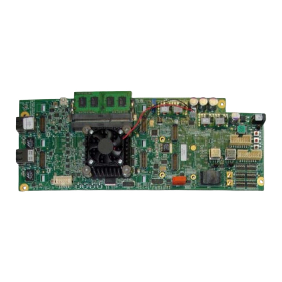
Page 7: Schematic Cs And Ps Views
MPC8569E-MDS-PB Schematic CS and PS Views MPC8569E-MDS-PB Schematic CS and PS Views Figure 2. MPC8569E-MDS-PB Component Side (CS) View DDR2 TRIG_OUT VDD_REG DDR3 CORE_VOLT VDD_OUT ASLEEP I_CORE 2V5_GETH FSEL0 FSEL1 5V_IN PS-ISP SSC0 SSC1 5V_IN SERDES CLK REG_CFG GETH2 CLK PLL0... -
Page 8: Switch Default Settings
Switch Default Settings Switch Default Settings The MPC8569E-MDS-PB has dual-in-line package (DIP) switches; see Figure 5. Default DIP switch positions establish MPC8569E-MDS-PB clock modes; see Table 4. NOTE! Ensure DIP switches are set according to default values. Table 4. MPC8569E-MDS-PB Default Configurations... - Page 9 SW5.8: Disables DDR2 Phase Reset Logic • ‘0’: DDR controller disables MCKE at reset; a few cycles later MCK is disabled. • ’1’: (Default) At reset, DDR controller simultaneously disables MCK and MCKE. MPC8569E-MDS-PB Hardware Getting Started, Rev. 3.1 Freescale Semiconductor...
- Page 10 • ’1’: (Default) QUICC Engine UCC1&3 GB Ethernet interface operates at 2.5V. SW6.8: QE UCC2 and UCC4 Voltage Select • ‘0’: QUICC Engine UCC2&4 GB Ethernet interface operates at 3.3V. • ’1’: (Default) QUICC Engine UCC2&4 GB Ethernet interface operates at 2.5V. MPC8569E-MDS-PB Hardware Getting Started, Rev. 3.1 Freescale Semiconductor...
- Page 11 (Default) 2:1 5:2 (2.5:1) 7:2 (3.5:1) SW7.8: SerDes Reference Clock Configuration • ‘0’: SerDes expects a 125 MHz reference clock frequency. • ’1’: (Default) SerDes expects a 100 MHz reference clock frequency. MPC8569E-MDS-PB Hardware Getting Started, Rev. 3.1 Freescale Semiconductor...
- Page 12 • Regardless of host/agent mode configuration, unconnected cfg_device_ID_1[n] inputs default to ‘1’. SW8.8: RapidIO System Size • ‘0’: Large system size with a maximum of 65,536 devices. • ‘1’: (Default) Small system size with a maximum of 256 devices. MPC8569E-MDS-PB Hardware Getting Started, Rev. 3.1 Freescale Semiconductor...
- Page 13 • 11: (Default) I C ROMs not accessed. Boot sequencer is disabled. SW9.8: Reset Configuration Source • ‘0’: RCW is read through I • ‘1’: (Default) RCW is read through IO pin sampling. MPC8569E-MDS-PB Hardware Getting Started, Rev. 3.1 Freescale Semiconductor...
- Page 14 • ‘1’: (Default) PLL parameters are controlled by plugs. SW10.8: Fuse Read Enable • ‘0’: Fuse reads are disabled during the reset sequence. • ‘1’: (Default) Fuse reads are enabled during reset sequence. MPC8569E-MDS-PB Hardware Getting Started, Rev. 3.1 Freescale Semiconductor...
-
Page 15: Connector Default Settings
Connector Default Settings Connector Default Settings The below table, Table 5, lists factory default connector, header, and socket settings for the MPC8569E-MDS-PB. Figure 6 marks the location of the listed connector types. Table 5. MPC8569E-MDS-PB Connector Default Settings Type Description... - Page 16 Connector Default Settings Table 5. MPC8569E-MDS-PB Connector Default Settings Type Description Function 16-pin Header CNTR ISP Used for BCSR programming. Socket NOR Flash Socket (Default) Insert NOR Flash device. U118 Socket NAND Flash Socket; located on PS. (Default) Insert NAND Flash device.
-
Page 17: Push Buttons
Push Buttons Push Buttons Table 6 lists the functioning of MPC8569E-MDS-PB push buttons. Table 6. MPC8569E-MDS-PB Push Buttons Push Button Position Description & Default • Press SW2 to Power-ON/OFF all PB components. SW2: POWER-ON/OFF • Powered from an external 5V power supply via the P2 power jack. -
Page 18: Led Lights
LED Lights LED Lights Table 7, below, lists the functioning of MPC8569E-MDS-PB LED lights. See Figure 8 for LED locations. Table 7. MPC8569E-MDS-PB LEDs Name Color LED ON LED OFF GETH2 Orange • GETH2 enabled. BCSR8-[0] is high. • BCSR8-[0] is low. -
Page 19: Board Control Status Registers (Bcsr)
• 1: DDR clock frequency is > or = 500MHz. • 1: At reset, DDR disables both MCK and MCKE. SW5[8] sampled at DDR_FIX • 0: DDR disables MCKE at reset; a few cycles later MCK HRESET [1] is disabled. MPC8569E-MDS-PB Hardware Getting Started, Rev. 3.1 Freescale Semiconductor... - Page 20 Boot Sequencer • Allows Boot Sequencer to load serial ROM (on I SW9[6:7] sampled [5:6] CFG_BOOT_SEQ[0:1] port) configuration data before the host configures the at HRESET [11] MPC8569E. MPC8569E-MDS-PB Hardware Getting Started, Rev. 3.1 Freescale Semiconductor...
- Page 21 • 0: Disable UPC1 OR enable TDM1A, TDM1B, UPC1_EN TDM1E, TDM1F, TDM1G, TDM1H, TDM2A, TDM2C, TDM2D, TDM2E, RMII5, RMII7, RMII8, TDM2G, TDM2F, and RMII6 • 1: Enable UPC1POS RUPC1POS_EN • 0: Disable UPC1POS OR enable TDM2A and TDM1B MPC8569E-MDS-PB Hardware Getting Started, Rev. 3.1 Freescale Semiconductor...
- Page 22 • 0: Reset (nMVRST) Marvel UCC1 and UCC2 • BRD (EEPROM I C Memory): write protected for I BRDWP Flash • 0: Not protected • 1: Not protected. BOOTWP • Boot write protected MPC8569E-MDS-PB Hardware Getting Started, Rev. 3.1 Freescale Semiconductor...
- Page 23 • If UCC3_GETH = 0 – then bit = 1 enables UCC3_RMII on PIB – then bit =0 enables TDM1C and UPC1_DEV2 UCC3_RMII • If UCC3_GETH = 1 – then bit has no effect MPC8569E-MDS-PB Hardware Getting Started, Rev. 3.1 Freescale Semiconductor...
- Page 24 • 0: Micrel PHY Reset on both UCC3- & UCC4-connected RnMICRST UEMs • 1: Normal operation • 1: Marvell PHY, UCC3 & UCC4 have 25MHz input on RMV_SEL_FREQ_34 • 0: Marvell PHY, UCC3 & UCC4 have 125MHz input on MPC8569E-MDS-PB Hardware Getting Started, Rev. 3.1 Freescale Semiconductor...
- Page 25 • 1: Enable RMII6 (on PIB) and TDM2F RMII6 • 0: Disable RMII6 AND enable ATM or POS • 1: Enable RMII8 (on PIB) RMII8 • 0: Disable RMII8 AND enable TDM1H MPC8569E-MDS-PB Hardware Getting Started, Rev. 3.1 Freescale Semiconductor...
- Page 26 • 0: Not present UEM inserted into J5 PRESENCE 4 • 1: Present • 0: Not present 10.16 BCSR15 Table 23. BCSR15 Register Config Signals Function Default • 1: Enable G3ENA_XC • 0: Disable MPC8569E-MDS-PB Hardware Getting Started, Rev. 3.1 Freescale Semiconductor...
- Page 27 • 1: Enable UPC1 Device2 • 0: Disable UPC1 Device 2 OR enable RMII3 on PIB,TDM1C and TDM2C TDM1C_DEV2 • If bit = 0 then RMII3 is enabled • Dev2- RxEN_B[2] • TDM2c-TSYNC • TDM1c RESERVED MPC8569E-MDS-PB Hardware Getting Started, Rev. 3.1 Freescale Semiconductor...
- Page 28 Table 26. BCSR18 Register Config Signals Function Value • BCSR revision [0:3] current version • Four bit revision coding • BCSR SUB revision [4:7] SUBREV sub version • Four bit revision coding MPC8569E-MDS-PB Hardware Getting Started, Rev. 3.1 Freescale Semiconductor...
-
Page 29: Memory Map
Access to MPC8569 memory slaves is controlled by the MPC8569 memory controller. Table 27 is only a recommended memory map; it is a "soft" map device. Users are free to move addresses around the map. MPC8569E-MDS-PB Memory Map (with NOR Flash as Boot Source Table 27. ADDRESS RANGE Block... -
Page 30: Working Environment
Working Environment 12 Working Environment Table 28. MPC8569E-MDS-PB Working Environment Modes Mode Optional Expansion Description Includes the noted modules: • PB powered, via P2, by an external • GETH3 & 4 UEM 5V power supply (included in kit). Standalone • SerDes Lane e, f SRIOx1 or UEM (SGMII mode) •... -
Page 31: Getting Started Procedures
Getting Started Procedures 13 Getting Started Procedures This section outlines “Getting Started” procedures for the MPC8569E-MDS-PB including use of the JTAG connectivity unit. Optional modules are detailed in Section 12. Procedure 1: Check hardware kit contents (Section 4). Procedure 2: Check PB default switch settings (Section 6). - Page 32 ETH cables with RJ45 connectors to the Ethernet ports: – J14 for GETH1 – J6 for GETH2 FSL Adaptor 5. Continue as per CodeWarrior Kit (with COM1/2) Configuration Guide instructions. RS-232 (male) MPC8569E-MDS-PB Hardware Getting Started, Rev. 3.1 Freescale Semiconductor...
-
Page 33: Serdes-Module Set-Ups
SGMII SGMII x2 PEX x2 PEX PEX at 2.5Gbaud PEX at 2.5Gbaud x1 SRIO2 x1 SRIO1 x1 PEX x1 PEX 2.5Gbaud 2.5Gbaud x1 SRIO2 x1 SRIO1 x2 PEX x2 PEX 2.5Gbaud 2.5Gbaud MPC8569E-MDS-PB Hardware Getting Started, Rev. 3.1 Freescale Semiconductor... - Page 34 SerDes Option 3: two UEM & one PEXx2 (x2 mode) a) Repeat first three steps of Option 2. See SerDes Option 2 photos. b) PEX slot now available as RC port x2. MPC8569E-MDS-PB Hardware Getting Started, Rev. 3.1 Freescale Semiconductor...
- Page 35 SerDes Option 5: two SRIOx1 & one PEXx2 (x2 mode) a) Repeat first three steps of Option 4. See SerDes Option 4 photos. b) PEX slot now available as RC port x2. MPC8569E-MDS-PB Hardware Getting Started, Rev. 3.1 Freescale Semiconductor...
- Page 36 SerDes Module Set-ups MPC8569E-MDS-PB Hardware Getting Started, Rev. 3.1 Freescale Semiconductor...
-
Page 37: How To Reach Us
Web Support: http://www.freescale.com/support Freescale Semiconductor reserves the right to make changes without further notice to any USA/Europe or Locations Not Listed: products herein. Freescale Semiconductor makes no warranty, representation or guarantee Freescale Semiconductor, Inc. - Page 38 SerDes Module Set-ups MPC8569E-MDS-PB Hardware Getting Started, Rev. 3.1 Freescale Semiconductor...
Need help?
Do you have a question about the MPC8569E-MDS-PB and is the answer not in the manual?
Questions and answers