Table of Contents
Advertisement
Quick Links
Mercury+ KX2 FPGA Module
Purpose
The purpose of this document is to present the characteristics of Mercury+ KX2 FPGA module to the user,
and to provide the user with a comprehensive guide to understanding and using the Mercury+ KX2 FPGA
module.
Summary
This document first gives an overview of the Mercury+ KX2 FPGA module followed by a detailed description
of its features and configuration options. In addition, references to other useful documents are included.
Product Information
Product
Document Information
Reference / Version / Date
Approval Information
Written by
Verified by
Approved by
User Manual
Code
ME-KX2
Reference
D-0000-430-002
Name
DIUN
GLAC
DIUN
Enclustra GmbH – Räffelstrasse 28 – CH-8045 Zürich – Switzerland
Name
Mercury+ KX2 FPGA Module
Version
06
Position
Design Engineer
Design Expert
Manager, BU SP
Phone +41 43 343 39 43 – www.enclustra.com
Date
25.07.2019
Date
10.06.2016
05.07.2016
25.07.2019
Advertisement
Chapters
Table of Contents

Subscribe to Our Youtube Channel
Related Manuals for Enclustra Mercury+ KX2


Summary of Contents for Enclustra Mercury+ KX2
- Page 1 Mercury+ KX2 FPGA Module User Manual Purpose The purpose of this document is to present the characteristics of Mercury+ KX2 FPGA module to the user, and to provide the user with a comprehensive guide to understanding and using the Mercury+ KX2 FPGA module.
- Page 2 Unauthorized duplication of this document, in whole or in part, by any means is prohibited without the prior written permission of Enclustra GmbH, Switzerland. Although Enclustra GmbH believes that the information included in this publication is correct as of the date of publication, Enclustra GmbH reserves the right to make changes at any time without notice.
-
Page 3: Table Of Contents
Table of Contents Overview General ........... 1.1.1 Introduction . - Page 4 3.11 Enclustra Module Configuration Tool ........40 I2C Communication Overview .
-
Page 5: Overview
Warning! It is possible to mount the Mercury+ KX2 FPGA module the wrong way round on the base board - always check that the mounting holes on the base board are aligned with the mounting holes of the Mercury+ KX2 FPGA module. -
Page 6: Electrostatic Discharge
ESD-protected environment. 1.1.7 Electromagnetic Compatibility The Mercury+ KX2 FPGA module is a Class A product and is not intended for use in domestic environments. The product may cause electromagnetic interference, for which appropriate measures must be taken. Features Xilinx Kintex-7 28 nm FPGA XC7K160T/XC7K325T/XC7K410T, FFG676/FBG676 package 256 user I/Os up to 3.3 V... -
Page 7: Mercury+ Pe1 Base Board
Xilinx Tool Support The FPGA devices equipped on the Mercury+ KX2 FPGA module are supported by the Vivado HL WebPACK Edition or by the Vivado HL Design Edition software, depending on the device’s density. Table 1 presents the correspondence between devices and tools. -
Page 8: Module Description
Figure 1: Hardware Block Diagram The main component of the Mercury+ KX2 FPGA module is the Xilinx Kintex-7 FPGA device. Most of its I/O pins are connected to the Mercury module connectors, making 216 regular user I/Os available to the user. -
Page 9: Module Configuration And Product Codes
Figure 2: Product Code Fields Please note that for the first revision modules or early access modules, the product code may not respect entirely this naming convention. Please contact Enclustra for details on this aspect. Article Numbers and Article Codes Every module is uniquely labeled, showing the article number and serial number. -
Page 10: Module Label
The correspondence between article number and article code is shown in Table 3. The article code repre- sents the product code, followed by the revision; the R suffix and number represent the revision number. The revision changes and product known issues are described in the Mercury+ KX2 FPGA Module Known Issues and Changes document [6]. -
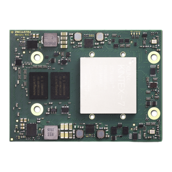
Page 11: Top And Bottom Views
Top and Bottom Views 2.4.1 Top View Figure 4: Module Top View 2.4.2 Bottom View Figure 5: Module Bottom View Please note that depending on the hardware revision and configuration, the module may look slightly dif- ferent than shown in this document. D-0000-430-002 11 / 48 Version 06, 25.07.2019... -
Page 12: Top And Bottom Assembly Drawings
Top and Bottom Assembly Drawings 2.5.1 Top Assembly Drawing Figure 6: Module Top Assembly Drawing 2.5.2 Bottom Assembly Drawing Figure 7: Module Bottom Assembly Drawing Please note that depending on the hardware revision and configuration, the module may look slightly dif- ferent than shown in this document. -
Page 13: Module Footprint
Figure 8: Module Footprint - Top View Warning! It is possible to mount the Mercury+ KX2 FPGA module the wrong way round on the base board - always check that the mounting holes on the base board are aligned with the mounting holes of the Mercury+ KX2 FPGA module. -
Page 14: Mechanical Data
Mechanical Data Table 4 describes the mechanical characteristics of the Mercury+ KX2 FPGA module. A 3D model (PDF) and a STEP 3D model are available [8], [9]. Symbol Value Size 54 mm Component height top 3.0 mm Component height bottom 1.3 mm... -
Page 15: User I/O
User I/O 2.9.1 Pinout Information on the Mercury+ KX2 FPGA module pinout can be found in the Enclustra Mercury Master Pinout [11], and in the additional document Enclustra Module Pin Connection Guidelines [10]. Warning! Please note that the pin types on the schematics symbol of the module connector and in the Master Pinout document are for reference only. -
Page 16: Differential I/Os
The information regarding the length of the signal lines from the FPGA device to the module connector is available in Mercury+ KX2 FPGA Module IO Net Length Excel Sheet [3]. This enables the user to match the total length of the differential pairs on the base board if required by the application. -
Page 17: Vref Usage
FPGA device, as well as other devices on the Mercury+ KX2 FPGA module. Do not leave a VREF pin floating when the used I/O standard requires a reference voltage, as this may damage the equipped FPGA device, as well as other devices on the Mercury+ KX2 FPGA module. 2.9.5... - Page 18 VCCO (if VCC_CFG_B14 is 2.5 V or 3.3 V). If the Mercury+ KX2 FPGA module is used in combination with a base board having only two module connectors, the VCC_IO_B13 pin that powers I/O bank 13 is connected to the on-board generated 1.8 V supply voltage.
-
Page 19: Signal Terminations
Internal differential termination is available only for certain VCCO voltages; please refer to Xilinx AR# 43989 for details. Single-Ended Outputs There are no series termination resistors on the Mercury+ KX2 FPGA module for single-ended outputs. If required, series termination resistors may be equipped on the base board (close to the module pins). 2.9.7 Analog Inputs The Kintex-7 FPGA devices provide a dual 12-bit ADC. -
Page 20: Multi-Gigabit Transceiver (Mgt)
Table 10: MGT Switching Characteristics on the Mercury+ KX2 FPGA module Warning! The maximum data rate on the MGT lines on the Mercury+ KX2 FPGA module depends on the routing path for these signals. Adequate signal integrity over the full signal path must be ensured when using MGTs at high performance rates. -
Page 21: Power
Power Generation Overview The Mercury+ KX2 FPGA module uses a 5 - 15 V DC power input for generating the on-board supply volt- ages (1.0 V, 1.2 V, 1.35 V/1.5 V, 1.8 V, 2.0 V, 2.5 V and 3.3 V). Some of these voltages (1.8 V, 2.5 V, 3.3 V) are accessible on the module connector. -
Page 22: Voltage Supply Inputs
Figure 10. 2.11.3 Voltage Supply Inputs Table 13 describes the power supply inputs on the Mercury+ KX2 FPGA module. The VCC voltages used as supplies for the I/O banks are described in Section 2.9.5. Pin Name Module Connector Pins... -
Page 23: Power Consumption
FPGA is adequately cooled. Table 15 lists the heat sink and thermal pad part numbers that are compatible with the Mercury+ KX2 FPGA module. Details on these parts and additional information that may assist in selecting a suitable heat sink for the Mercury+ KX2 FPGA module can be found in the Enclustra Modules Heat Sink Application Note [15]. -
Page 24: Clock Generation
Table 16: Voltage Monitoring Outputs 2.12 Clock Generation A 100 MHz single-ended oscillator and a 200 MHz LVDS oscillator are equipped on the Mercury+ KX2 FPGA module. The reference clock inputs for the MGT transceivers are available on the module connector pins. Signal Name... -
Page 25: Leds
DDR3 SDRAM The DDR3 SDRAM on the Mercury+ KX2 FPGA module is operated at 1.35 V (low power mode) or at 1.5 V, depending on a selection signal. Four 16-bit memory chips are used to build a 64-bit wide memory. -
Page 26: Signal Description
Please check the user manual regularly for updates. Any parts with different speed bins or temperature ranges that fulfill the requirements for the module variant may be used. 2.15.2 Signal Description Please refer to the Mercury+ KX2 FPGA Module FPGA Pinout Excel Sheet [4] for detailed information on the DDR3 SDRAM connections. 2.15.3 Termination Warning! No external termination is implemented for the data signals on the Mercury+ KX2 FPGA module. -
Page 27: Ddr3 Low Voltage Operation
512 Mbit Cypress (Spansion) Table 22: QSPI Flash Types Warning! Other flash memory devices may be equipped in future revisions of the Mercury+ KX2 FPGA module. Please check the user manual regularly for updates. D-0000-430-002 27 / 48 Version 06, 25.07.2019... -
Page 28: Signal Description
FPGA and the flash device. 2.17 Dual Gigabit Ethernet Two 10/100/1000 Mbit Ethernet PHYs are available on the Mercury+ KX2 FPGA module, connected to the FPGA via RGMII interfaces. 2.17.1 Ethernet PHY Type Table 24 describes the equipped Ethernet PHY device type on the Mercury+ KX2 FPGA module. -
Page 29: Signal Description
For the Ethernet PHY configuration via the MDIO interface, the MDC clock frequency must not exceed 1 MHz. 2.18 FTDI USB 2.0 Controller The Mercury+ KX2 FPGA module features an FTDI USB 2.0 controller, which allows data transfers to a host computer using speeds of up to 40 MB/s. D-0000-430-002 29 / 48... -
Page 30: Ftdi Type
Please note that when using the synchronous FIFO interface, in certain temperature conditions, the timing path requirement between FPGA and FTDI device is not met. For details on FTDI interface pinout, please refer to the Mercury+ KX2 FPGA Module FPGA Pinout Excel Sheet [4] and Mercury+ KX2 FPGA Module User Schematics [5]. -
Page 31: Device Configuration
3 Device Configuration Configuration Signals Table 28 describes the most important configuration pins. Some of the pins are connected to a user I/O, as well as to a special purpose configuration pin. This is done for compatibility with other Mercury modules, on which the configuration pins can be used as user I/Os after configuration. -
Page 32: Module Connector C Detection
All configuration signals except for FPGA_MODE must be high impedance as soon as the device is released from reset. Violating this rule may damage the equipped FPGA device, as well as other devices on the Mercury+ KX2 FPGA module. Module Connector C Detection Signal C_PRSNT# (pin C-167) must be connected to GND on the base board if the designed base board has three connectors. -
Page 33: Pull-Up During Configuration
Pull-Up During Configuration The Pull-Up During Configuration signal (PUDC) is pulled to GND on the module; as PUDC is an active-low signal, all FPGA I/Os will have the internal pull-up resistors enabled during device configuration. If the application requires the pull-up during configuration to be disabled, this can be achieved by removing R202 component and by mounting R203 - in this configuration the PUDC pin is connected to VCC_CFG_B14. -
Page 34: Jtag On Module Connector
Xilinx JTAG Adapter The Mercury+ KX2 FPGA module is equipped with a Xilinx JTAG adapter implemented using the FTDI device. Port A of the FTDI device can be configured in synchronous FIFO mode or in Xilinx JTAG mode; please refer to Section 3.10 for details. -
Page 35: Signal Description
3.6.1 Signal Description Signal Name Description FLASH_CLK_FPGA_CCLK Must be high impedance during configuration and operation FLASH_DO_FPGA_DIN Must be high impedance during configuration and operation FPGA_INIT# Is pulled low by the FPGA if any CRC error occurs during the configuration; it may be used as an input to delay the start of the FPGA configuration. -
Page 36: Qspi Flash Programming Via Jtag
Figure 13: QSPI Flash Programming from an External SPI Master - Signal Diagrams Warning! Accessing the QSPI flash directly without putting the FPGA device into reset may damage the equipped FPGA device, as well as other devices on the Mercury+ KX2 FPGA module. D-0000-430-002 36 / 48... -
Page 37: Signal Description
3.9.1 Signal Description Signal Name QSPI Flash Pin Description FLASH_CLK_FPGA_CCLK SPI CLK FLASH_DO_FPGA_DIN SO/IO1 SPI MISO FPGA_PROG# Must be pulled low during QSPI flash programming. When released, all other pins of the SPI interface must be high impedance. FLASH_DI SI/IO0 SPI MOSI FLASH_CS# SPI CS#... -
Page 38: Ftdi Port B Configuration
3.10.2 FTDI Port B Configuration FTDI_MODE1 FTDI_MODE0 FPGA_MODE FPGA_PROG# Configuration (BCBUS6) (BCBUS5) (BCBUS4) (BCBUS3) HiZ (1) Slave serial configuration via FTDI FTDI device pins connected to module I2C bus QSPI flash programming via FTDI HiZ (1) Master serial configuration (FPGA is configured from QSPI flash) HiZ (1) FTDI device pins connected to... -
Page 39: Fpga Slave Serial Configuration Via Ftdi
Accessing the QSPI flash directly without putting the FPGA device into reset may damage the equipped FPGA device, as well as other devices on the Mercury+ KX2 FPGA module. On revision 1 modules, this signal must have a value of 1. -
Page 40: Enclustra Module Configuration Tool
3.11 Enclustra Module Configuration Tool The QSPI flash on the Mercury+ KX2 FPGA module can be programmed via FTDI using the Enclustra Module Configuration Tool (MCT) [14]. Slave serial configuration is also supported by the Enclustra MCT software. D-0000-430-002 40 / 48... -
Page 41: I2C Communication
4 I2C Communication Overview The I2C bus on the Mercury+ KX2 FPGA module is connected to the FPGA device, EEPROM and FTDI USB 2.0 controller, and is available on the module connector. This allows external devices to read the module type and to connect more devices to the I2C bus. -
Page 42: Secure Eeprom
An example demonstrating how to read the module information from the EEPROM memory is included in the Mercury+ KX2 FPGA module reference design. Warning! The secure EEPROM is for Enclustra use only. Any attempt to write data to the secure EEPROM causes the warranty to be rendered void. 4.4.1... -
Page 43: Fpga Device Types
Module Configuration Addr. Bits Comment Min. Value Max. Value Comment FPGA Type See FPGA type table (Table 43) 0x08 FPGA device speed grade Temperature range 0 (Commercial) 1 (Industrial) Power grade 0 (Normal) 1 (Low Power) Gigabit Ethernet port count 0x09 Reserved RTC equipped... -
Page 44: Operating Conditions
5 Operating Conditions Absolute Maximum Ratings Table 44 indicates the absolute maximum ratings for Mercury+ KX2 FPGA module. The values given are for reference only; for details please refer to the Kintex-7 Datasheet [18]. Symbol Description Rating Unit VCC_MOD Supply voltage relative to GND -0.5 to 16... -
Page 45: Ordering And Support
6 Ordering and Support Ordering Please use the Enclustra online request/order form for ordering or requesting information: http://www.enclustra.com/en/order/ Support Please follow the instructions on the Enclustra online support site: http://www.enclustra.com/en/support/ D-0000-430-002 45 / 48 Version 06, 25.07.2019... - Page 46 ADC Parameters ..........20 MGT Switching Characteristics on the Mercury+ KX2 FPGA module ....20 Generated Power Supplies .
- Page 47 I2C Addresses ..........41 EEPROM Sector 0 Memory Map .
- Page 48 [1] Enclustra General Business Conditions http://www.enclustra.com/en/products/gbc/ [2] Mercury+ KX2 FPGA Module Reference Design Ask Enclustra for details [3] Mercury+ KX2 FPGA Module IO Net Length Excel Sheet Ask Enclustra for details [4] Mercury+ KX2 FPGA Module FPGA Pinout Excel Sheet Ask Enclustra for details...
Need help?
Do you have a question about the Mercury+ KX2 and is the answer not in the manual?
Questions and answers