
Subscribe to Our Youtube Channel
Related Manuals for ADLINK Technology DLAP-211-Nano Series


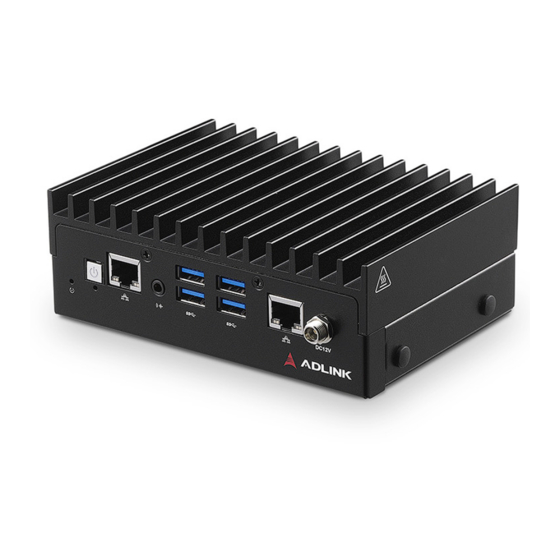
Summary of Contents for ADLINK Technology DLAP-211-Nano Series
- Page 1 DLAP-211-JNX / DLAP-211-JT2 / DLAP-211-Nano Series Edge Inference System User’s Manual Manual Rev.: Revision Date: November 9, 2022 Part No: 50M-00016-1010...
- Page 2 Revision History Revision Release Date Description of Change(s) 2021-12-06 Initial Release 2022-11-09 Added DLAP-211-JT2 Revision History...
-
Page 3: Preface
DLAP-211-JNX / DLAP-211-JT2 / DLAP-211-Nano Series Preface Copyright © 2022 ADLINK Technology, Inc. This document contains proprietary information protected by copy- right. All rights are reserved. No part of this manual may be repro- duced by any mechanical, electronic, or other means in any form without prior written permission of the manufacturer. - Page 4 Conventions Take note of the following conventions used throughout this manual to make sure that users perform certain tasks and instructions properly. Additional information, aids, and tips that help users perform tasks. NOTE: NOTE: Information to prevent minor physical injury, component dam- age, data loss, and/or program corruption when trying to com- plete a task.
-
Page 5: Table Of Contents
DLAP-211-JNX / DLAP-211-JT2 / DLAP-211-Nano Series Table of Contents Revision History..............ii Preface ..................iii List of Tables................. vii List of Figures ................ ix 1 Introduction ................ 1 Features................1 Specifications............... 2 Mechanical Dimensions............5 External Layout..............7 Pin Definitions..............10 1.5.1... - Page 6 VESA Mount ..............24 DIN Rail Mount..............25 AT Power Mode Switch (SW4) .......... 26 3 Using the System.............. 27 Software Configuration ............27 System Recovery............... 27 COM Port Configuration............. 29 SPI, I2C, and Relay Configuration ........30 3.4.1 GPIO................. 30 3.4.2 SPI, I2C, Relay ............
-
Page 7: List Of Tables
DLAP-211-JNX / DLAP-211-JT2 / DLAP-211-Nano Series List of Tables Table 1-1: Specifications ............. 2 Table 1-2: Front Panel I/O Connectors & Controls ...... 8 Table 1-3: Rear Panel I/O Connectors ........9 Table 1-4: NX/TX2NX/Nano Module & I210 LAN LED ....10 Table 1-5: RJ45 GbE Pin Definition........... - Page 8 This page intentionally left blank. viii List of Tables...
-
Page 9: List Of Figures
DLAP-211-JNX / DLAP-211-JT2 / DLAP-211-Nano Series List of Figures Figure 1-1: DLAP-211-Nano/JT2/NX Front View ......5 Figure 1-2: DLAP-211-Nano/JT2/NX Side View ......5 Figure 1-3: DLAP-211-NanoS/JT2S/NXS Front View....6 Figure 1-4: DLAP-211-NanoS/JT2S/NXS Side View ....6 Figure 1-5: DLAP-211-NanoS/JT2S/NXS Front Panel I/O Connec- tors 1................ - Page 10 This page intentionally left blank. List of Figures...
-
Page 11: Introduction
DLAP-211-JNX / DLAP-211-JT2 / DLAP-211-Nano Series Introduction ADLINK’s DLAP-211 Series Edge Inference System leverages the power of NVIDIA® Jetson™ Nano TX2NX, and NX modules to deliver artificial intelleigence (AI) at the edge. The DLAP-211 Edge AI Platforms with integrated NVIDIA Jetson accelerates deep... -
Page 12: Specifications
1.2 Specifications The DLAP-211 series come in six versions supporting Jetson Nano, TX2NX, and NX modules along with different I/O expansion options. DLAP-211- DLAP-211- DLAP-211- DLAP-211- DLAP-211- DLAP-211- Model JNXS JT2S NanoS NanoS System NVIDIA Maxwell 384-core NVIDIA Volta NVIDIA Pascal GPU with 48 Tensor Architecture GPU with architecture with 128... - Page 13 DLAP-211-JNX / DLAP-211-JT2 / DLAP-211-Nano Series DLAP-211- DLAP-211- DLAP-211- DLAP-211- DLAP-211- DLAP-211- Model JNXS JT2S NanoS NanoS Extension Slots Mini PCIe 1x Mini PCIe slot 1x M.2 B key 2242 socket SD Card Slot 1x SD card slot Power Supply...
- Page 14 DLAP-211- DLAP-211- DLAP-211- DLAP-211- DLAP-211- DLAP-211- Model JNXS JT2S NanoS NanoS Shock Operating 100G, half sine 11 ms duration w/ SD, mSATA Contact +/- 4kV, Air +/- 8kV CE & FCC class B, (EN61000-6-4/-6-2), CE-LVD & UL by CB, FCCID Regulatory (DLAP-211-JNXO &...
-
Page 15: Mechanical Dimensions
DLAP-211-JNX / DLAP-211-JT2 / DLAP-211-Nano Series 1.3 Mechanical Dimensions All dimensions shown in millimeters (mm). Figure 1-1: DLAP-211-Nano/JT2/NX Front View Figure 1-2: DLAP-211-Nano/JT2/NX Side View Introduction... -
Page 16: Figure 1-3: Dlap-211-Nanos/Jt2S/Nxs Front View
Figure 1-3: DLAP-211-NanoS/JT2S/NXS Front View Figure 1-4: DLAP-211-NanoS/JT2S/NXS Side View Introduction... -
Page 17: External Layout
DLAP-211-JNX / DLAP-211-JT2 / DLAP-211-Nano Series 1.4 External Layout DLAP-211-NanoS/JT2S/NXS Front Panel Figure 1-5: DLAP-211-NanoS/JT2S/NXS Front Panel I/O Connectors 1 DLAP-211-NanoS/JT2S/NXS Front Panel Figure 1-6: DLAP-211-NanoS/JT2S/NXS Front Panel I/O Connectors 2 Introduction... -
Page 18: Table 1-2: Front Panel I/O Connectors & Controls
Item Name Description The power button is a non-latched pushbutton with a blue LED power indicator. Press to power on/power off the system. The button LED lights up Power button when the system is turned on. If the system hangs, pressing and holding the button continuously for 5 seconds performs a hard shutdown on the system. -
Page 19: Table 1-3: Rear Panel I/O Connectors
DLAP-211-JNX / DLAP-211-JT2 / DLAP-211-Nano Series Rear Panel Figure 1-7: Rear Panel I/O Connectors Item Name Description CAN bus CAN 2.0B (backward compatible with 2.0A) COM port (DB-9 connector) Serial port RS-232/422/485 (software programmable) HDMI port HDMI 2.0 with lock USB 2.0... -
Page 20: Pin Definitions
1.5 Pin Definitions 1.5.1 Ethernet GbE Connectors The DLAP-211 series comes with two RJ45 connectors: NVIDIA® Jetson™ modules (LAN 1) Intel® I210 (LAN 2) LAN LED connection speed color indicators: Active & Link Speed (Left LED) (Right LED) 10 Mbps Yellow (Blinking) 100 Mbps... -
Page 21: Usb 3.0 Connectors
DLAP-211-JNX / DLAP-211-JT2 / DLAP-211-Nano Series 1.5.2 USB 3.0 Connectors The USB 3.0 ports support a USB Type-A connection, compatible with SuperSpeed, Hi-Speed, Full-speed, and Low-speed USB devices suitable for USB peripherals including USB cameras. Pin # Signal Name USB3.0_P5VA... -
Page 22: Controller Area Network (Can) Bus
1.5.4 Controller Area Network (CAN) Bus The Controller Area Network (CAN) enables communication among devices. Signal Description (Not connected) CAN0_Low Differential CAN signal negative level (Not connected) (Not connected) (Not connected) (Not connected) CAN0_High Differential CAN signal positive level (Not connected) (Not connected) Table 1-7: CAN Bus Pin Definition 1.5.5... -
Page 23: Hdmi Connectors
DLAP-211-JNX / DLAP-211-JT2 / DLAP-211-Nano Series 1.5.6 HDMI Connectors The rear panel HDMI connector supports HDMI 2.0. Pin # Signal Pin # Signal TMDS Data2+ TMDS Data2 Shield TMDS Data2– TMDS Data1+ TMDS Data1 Shield TMDS Data1– TMDS Data0+ TMDS Data0 Shield TMDS Data0–... -
Page 24: D-Sub 37-Pin Connector
1.5.8 D-sub 37-pin Connector Pin # Signal Voltage Pin # Signal Voltage OPEN Relay COM Relay SPI0_SCK 3.3V SPI0_CS1_1 3.3V SPI0_MOSI 3.3V SPI0_MISO 3.3V SPI0_CS0_L 3.3V (GPO1)GPIO_14 3.3V (GPO2)GPIO_12 3.3V (GPO3)GPIO_10 3.3V (GPO4)GPIO_06 3.3V (GPI1)GPIO_05 3.3V (GPI2)GPIO_04 3.3V (GPI3)GPIO_03 3.3V (GPI4)GPIO_02 3.3V JUMPER2_EN... -
Page 25: Side I/O Slots
DLAP-211-JNX / DLAP-211-JT2 / DLAP-211-Nano Series 1.5.9 Side I/O Slots The I/O connectors accessible from the right side panel of the DLAP-211 are described below. Figure 1-8: USIM / SD Side Door SD Card Slot For additional storage, use the side door to install or remove a user-provided SD card. - Page 26 Orientation Insert the SIM and SD cards with the orientations shown below. Introduction...
-
Page 27: Getting Started
DLAP-211-JNX / DLAP-211-JT2 / DLAP-211-Nano Series Getting Started 2.1 Unpacking Checklist Before unpacking, check the shipping carton for any damage. If the shipping carton and/or contents are damaged, inform your dealer immediately. Retain the shipping carton and packing materials for inspection. Obtain authorization from your dealer before returning any product to ADLINK. -
Page 28: Removing The Chassis Cover
2.3 Removing the Chassis Cover To access the DLAP-211’s internal components, remove the underside of the chassis as follows. 1. On the front panel, remove the nut and washer from the 12V DC connector and remove the two mounting screws, as indicated in the figure below. 2. - Page 29 DLAP-211-JNX / DLAP-211-JT2 / DLAP-211-Nano Series 3. Slide the cover in the direction indicated by the red arrow. 4. Lift the cover off of the chassis. Reverse the steps to replace the bottom cover. Getting Started...
-
Page 30: Installing An M.2 Ssd Module
2.4 Installing an M.2 SSD Module Use the following steps to install an M.2 SSD module. 1. Insert the M.2 2242 B or B+M key module into the indi- cated slot (under the wires) at an angle. Figure 2-1: M.2 2242 B Key Slot 2. -
Page 31: Installing A Mini Pcie Wi-Fi Module
DLAP-211-JNX / DLAP-211-JT2 / DLAP-211-Nano Series 2.5 Installing a Mini PCIe Wi-Fi Module Use the following steps to install a Mini PCIe Wi-Fi module. 1. Insert the Mini PCIe Wi-Fi module into the indicated slot at an angle. Figure 2-2: Mini PCIe Wi-Fi Slot 2. -
Page 32: Connecting Dc Power
2.6 Connecting DC Power Before providing DC power to the DLAP-211, ensure the volt- age and polarity provided are compatible with the DC input. Improper input voltage and/or polarity can be responsible for WARNING: system damage. Avant de connecter le PC DLAP-211 à une source de courant continu, veuillez vous assurer de la polarité... - Page 33 DLAP-211-JNX / DLAP-211-JT2 / DLAP-211-Nano Series Les sources d'alimentation CC doivent être conformes aux circuits LPS et SELV (ES1) avecaucun risque énergétique, ainsi que: CEI 62368-1, CEI 60950-1 et UL 62368-1 Tension de sortie: 12V DC Courant de sortie: 5.0A minimum ...
-
Page 34: Vesa Mount
2.7 VESA Mount The DLAP-211 controller ships with a VESA 100 mounting bracket and four M4 screws. Follow the steps below to mount the device. 1. Attach the VESA bracket to the wall (or other suitable mounting surface) such that its keyhole-shaped mount- ing holes are oriented with the wider openings at the top. -
Page 35: Din Rail Mount
DLAP-211-JNX / DLAP-211-JT2 / DLAP-211-Nano Series 2.8 DIN Rail Mount The DLAP-211 controller may optionally include a DIN rail mount kit, with its own six M4 screws, in addition to the standard VESA mount kit. Follow these steps to install the DIN rail bracket. -
Page 36: At Power Mode Switch (Sw4)
2.9 AT Power Mode Switch (SW4) The DLAP-211 is set in AT mode by default. By using the AT Power Mode Switch (SW4), users can set the system to be pow- ered-on with the power button. Figure 2-5: AT Power Mode Switch (SW4) AT mode can be configured as follows. -
Page 37: Using The System
DLAP-211-JNX / DLAP-211-JT2 / DLAP-211-Nano Series Using the System 3.1 Software Configuration The DLAP-211 ships with a customized NVIDIA Linux for Tegra (L4T) image pre-installed. The latest version of this custom L4T image and other relevant files are available on the ADLINK web- site. -
Page 38: Figure 3-1: Successful Client/Host Connection
Host PC: 6. Connect the host PC to the client via OTG cable. 7. Open a terminal on the host PC and run this command: # lsusb 8. Look for “NVidia Corp.” in the output (an example is cir- cled in red in the screenshot below). If found, the host PC recognizes the client and you may proceed. -
Page 39: Com Port Configuration
DLAP-211-JNX / DLAP-211-JT2 / DLAP-211-Nano Series 3.3 COM Port Configuration By default, the DLAP-211 is configured to support the RS-232 pro- tocol. Model COM Port Name DLAP-211-JNX/JNXS ttyTHS0 DLAP-211-JT2/JT2S ttyTHS2 DLAP-211-Nano/NanoS ttyTHS1 Table 3-1: COM Port Names Switching between RS-232/422/485: $ echo rs232 >... -
Page 40: Spi, I2C, And Relay Configuration
3.4 SPI, I2C, and Relay Configuration The DLAP-211-JT2S, DLAP-211-NanoS, and DLAP-211-JNXS support I2C, SPI, GPIO, and Relay functions through a 37-pin D- sub connector that can be accessed through the commands described in the following sections. 3.4.1 GPIO DLAP-211-JNXS GPIO map table: Signal GPIO Number Pin Signal... -
Page 41: Spi, I2C, Relay
DLAP-211-JNX / DLAP-211-JT2 / DLAP-211-Nano Series Examples. GPO set low command: $echo 0 > /sys/class/gpio/gpio345/value GPI get value command: $cat /sys/class/gpio/gpio266/value 3.4.2 SPI, I2C, Relay DLAP-211-JNXS/JT2S/NanoS SPI, I2C, Relay map table: Model I2C Name SPI Name Relay GPIO Number /dev/spidev0.0... - Page 42 This page intentionally left blank. Using the System...
-
Page 43: Important Safety Instructions
DLAP-211-JNX / DLAP-211-JT2 / DLAP-211-Nano Series Important Safety Instructions For user safety, please read and follow all instructions, Warnings, Cautions, and Notes marked in this manual and on the associated device before handling/operating the device, to avoid injury or damage. - Page 44 Never attempt to repair the device, which should only be ser- viced by qualified technical personnel using suitable tools A Lithium-type battery may be provided for uninterrupted backup or emergency power. Risk of explosion if battery is replaced with one of an incorrect type;...
- Page 45 DLAP-211-JNX / DLAP-211-JT2 / DLAP-211-Nano Series Consignes de Sécurité Importantes Pour la sécurité de l'utilisateur, veuillez lire et suivre toutes les instructions, avertissements, mises en garde et notes indiquées dans ce manuel et sur les l'appareil avant de manipuler/d'utiliser l'appareil, afin d'éviter toute blessure ou dommage.
- Page 46 Installez/fixez et utilisez l'appareil uniquement sur des surfaces stables et/ou sur les fixations recommandées L'ordinateur Smart Touch est alimenté par un adaptateur ou une source CC. Veuillez vous assurer que l'adapta- teur ou la source CC doit conserver la connexion à la terre s'il est doté...
-
Page 47: Getting Service
DLAP-211-JNX / DLAP-211-JT2 / DLAP-211-Nano Series Getting Service Ask an Expert: http://askanexpert.adlinktech.com ADLINK Technology, Inc. No. 66, Huaya 1st Rd., Guishan Dist., Taoyuan City 333411, Taiwan Tel: +886-3-216-5088 Fax: +886-3-328-5706 Email: service@adlinktech.com Ampro ADLINK Technology, Inc. 6450 Via Del Oro...
Need help?
Do you have a question about the DLAP-211-Nano Series and is the answer not in the manual?
Questions and answers