
ADLINK Technology DLAP-211-JNX Series Manuals
Manuals and User Guides for ADLINK Technology DLAP-211-JNX Series. We have 2 ADLINK Technology DLAP-211-JNX Series manuals available for free PDF download: User Manual
ADLINK Technology DLAP-211-JNX Series User Manual (49 pages)
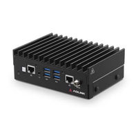
Edge Inference System
Brand: ADLINK Technology
|
Category: Computer Hardware
|
Size: 1 MB
Table of Contents
Advertisement
ADLINK Technology DLAP-211-JNX Series User Manual (47 pages)
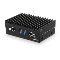
Edge Inference System
Brand: ADLINK Technology
|
Category: Desktop
|
Size: 4 MB
Table of Contents
Advertisement
Related Products
- ADLINK Technology DLAP-211-JNXS
- ADLINK Technology DLAP-211-JNXO
- ADLINK Technology DLAP-211-Nano Series
- ADLINK Technology DLAP-211-NanoO
- ADLINK Technology DLAP-211-Orin Series
- ADLINK Technology DLAP-211-Orin NX 8GB
- ADLINK Technology DLAP-211-Orin NX 16GB
- ADLINK Technology DLAP-211-Orin Nano 4GB
- ADLINK Technology DLAP-211-Orin NX S 8GB
- ADLINK Technology DLAP-211-Orin Nano S 4GB