Sign In
Upload
Manuals
Brands
ADLINK Technology Manuals
Desktop
DLAP-211-JT2
ADLINK Technology DLAP-211-JT2 Manuals
Manuals and User Guides for ADLINK Technology DLAP-211-JT2. We have
1
ADLINK Technology DLAP-211-JT2 manual available for free PDF download: User Manual
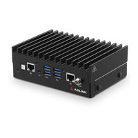
ADLINK Technology DLAP-211-JT2 User Manual (47 pages)
Edge Inference System
Brand:
ADLINK Technology
| Category:
Desktop
| Size: 4 MB
Table of Contents
Preface
3
Table of Contents
5
List of Tables
7
List of Figures
9
Introduction
11
Features
11
Specifications
12
Table 1-1: Specifications
12
Mechanical Dimensions
15
Figure 1-1: DLAP-211-Nano/Jt2/Nx Front View
15
Figure 1-2: DLAP-211-Nano/Jt2/Nx Side View
15
Figure 1-3: DLAP-211-Nanos/Jt2S/Nxs Front View
16
Figure 1-4: DLAP-211-Nanos/Jt2S/Nxs Side View
16
External Layout
17
Figure 1-5: DLAP-211-Nanos/Jt2S/Nxs Front Panel I/O Connec
17
Figure 1-6: DLAP-211-Nanos/Jt2S/Nxs Front Panel I/O Connec
17
Table 1-2: Front Panel I/O Connectors & Controls
18
Table 1-3: Rear Panel I/O Connectors
19
Figure 1-7: Rear Panel I/O Connectors
19
Pin Definitions
20
Ethernet Gbe Connectors
20
Table 1-4: Nx/Tx2Nx/Nano Module & I210 LAN LED
20
Table 1-5: RJ45 Gbe Pin Definition
20
USB 3.0 Connectors
21
DC Connector
21
Table 1-6: USB 3.0 Pin Definition
21
Controller Area Network (CAN) Bus
22
COM Port
22
Table 1-7: CAN Bus Pin Definition
22
Table 1-8: RS-232/422/485 Connector Pin Definition
22
HDMI Connectors
23
USB 2.0 OTG Connector
23
Table 1-9: HDMI Connector Pin Definition
23
Table 1-10: USB 2.0 OTG Connector Pin Information
23
D-Sub 37-Pin Connector
24
Table 1-11: D-Sub 37-Pin Pin Definition
24
Side I/O Slots
25
Figure 1-8: USIM / SD Side Door
25
Getting Started
27
Unpacking Checklist
27
Cooling Considerations
27
Removing the Chassis Cover
28
Installing an M.2 SSD Module
30
Figure 2-1: M.2 2242 B Key Slot
30
Installing a Mini Pcie Wi-Fi Module
31
Figure 2-2: Mini Pcie Wi-Fi Slot
31
Connecting DC Power
32
VESA Mount
34
Figure 2-3: VESA Mount
34
DIN Rail Mount
35
Figure 2-4: DIN Rail Mount
35
AT Power Mode Switch (SW4)
36
Table 2-1: at Mode Switch Configuration
36
Figure 2-5: at Power Mode Switch (SW4)
36
Using the System
37
Software Configuration
37
System Recovery
37
Figure 3-1: Successful Client/Host Connection
38
COM Port Configuration
39
Table 3-1: COM Port Names
39
SPI, I2C, and Relay Configuration
40
Gpio
40
Table 3-2: DLAP-211-JNXS GPIO Map Table
40
Table 3-3: DLAP-211-JT2S GPIO Map Table
40
Table 3-4: DLAP-211-Nanos GPIO Map Table
40
Table 3-5: DLAP-211-Nanos GPIO Map Table
40
SPI, I2C, Relay
41
Important Safety Instructions
43
Getting Service
47
Advertisement
Advertisement
Related Products
ADLINK Technology DLAP-211-JT2S
ADLINK Technology DLAP-401-Xavier
ADLINK Technology DLAP-3000-CF Series
ADLINK Technology DLAP-3000-CFP12
ADLINK Technology DLAP3100-CFP1
ADLINK Technology DLAP3100-CFP2
ADLINK Technology DLAP3100-CFT1
ADLINK Technology DLAP-3100-CFP12
ADLINK Technology DLAP-3100-CFP35
ADLINK Technology DLAP-211-JNX Series
ADLINK Technology Categories
Computer Hardware
Motherboard
PCI Card
Control Unit
Desktop
More ADLINK Technology Manuals
Login
Sign In
OR
Sign in with Facebook
Sign in with Google
Upload manual
Upload from disk
Upload from URL