Table of Contents
Advertisement
Quick Links
FEATURES
24-bit stereo audio ADC and DAC: >98 dB SNR
Sampling rates from 8 kHz to 96 kHz
Low power: 17 mW record, 18 mW playback, 48 kHz
6 analog input pins, configurable for single-ended or
differential inputs
Flexible analog input/output mixers
Stereo digital microphone input
Analog outputs: 2 differential stereo, 2 single-ended stereo,
1 mono headphone output driver
PLL supporting input clocks from 8 MHz to 27 MHz
Analog automatic level control (ALC)
Microphone bias reference voltage
Analog and digital I/O: 3.3 V
2
I
C and SPI control interfaces
Digital audio serial data I/O: stereo and time-division
multiplexing (TDM) modes
Software-controllable clickless mute
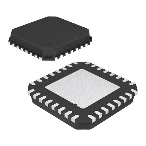
32-lead, 5 mm × 5 mm LFCSP
−40°C to +105°C operating temperature range
Qualified for automotive applications
APPLICATIONS
Automotive head units
Automotive amplifiers
Navigation systems
Rear-seat entertainment systems
Rev. 0
Information furnished by Analo
responsibility is assumed by Ana
rights of third parties that may re
license is granted by implication
Trademarks and registered trad
Downloaded from
Elcodis.com
electronic components distributor
FUNCTIONAL BLOCK DIAGRAM
JACKDET/MICIN
LAUX
LINP
INPUT
LINN
MIXERS
RINP
ALC
RINN
RAUX
MICROPHONE
MICBIAS
BIAS
MCLK ADC_SDATA
g Devices is believed to be accurate and reliable. However, no
log Devices for its use, nor for any infringements of patents or other
sult from its use. Specifications subject to change without notice. No
or otherwise under any patent or patent rights of Analog Devices.
emarks are the property of their respective owners.
Stereo, Low Power, 96 kHz, 24-Bit
Audio Codec with Integrated PLL
GENERAL DESCRIPTION
The ADAU1961 is a low power, stereo audio codec that supports
stereo 48 kHz record and playback at 35 mW from a 3.3 V analog
supply. The stereo audio ADCs and DACs support sample rates
from 8 kHz to 96 kHz as well as a digital volume control.
The record path includes an integrated microphone bias circuit
and six inputs. The inputs can be mixed and muxed before the
ADC, or they can be configured to bypass the ADC. The
ADAU1961 includes a stereo digital microphone input.
The ADAU1961 includes five high power output drivers (two
differential and three single-ended), supporting stereo head-
phones, an earpiece, or other output transducer. AC-coupled
or capless configurations are supported. Individual fine level
controls are supported on all analog outputs. The output mixer
stage allows for flexible routing of audio.
The serial control bus supports the I
serial audio bus is programmable for I
and TDM modes. A programmable PLL supports flexible clock
generation for all standard integer rates and fractional master
clocks from 8 MHz to 27 MHz.
HP JACK
REGULATOR
DETECTION
ADC
ADC
DAC
DIGITAL
DIGITAL
FILTERS
FILTERS
ADC
SERIAL DATA
PLL
INPUT/OUTPUT PORTS
DAC_SDATA
ADDR0/
CLATCH
Figure 1.
One Technology Way, P.O. Box 9106, Norwood,
Tel: 781.329.4700
Fax: 781.461.3113
ADAU1961
2
C and SPI protocols. The
2
S, left-/right-justified,
ADAU1961
LOUTP
LOUTN
DAC
LHP
OUTPUT
MONOOUT
MIXERS
RHP
DAC
ROUTP
ROUTN
2
I
C/SPI
CONTROL PORT
ADDR1/
SCL/
SDA/
CDATA
CCLK
COUT
MA 02062-9106, U.S.A.
©2010 Analog Devices,
www.analog.com
Inc. All rights reserved.
Advertisement
Table of Contents

Related Manuals for Analog Devices ADAU1961


Summary of Contents for Analog Devices ADAU1961
-
Page 1: Features
ADAU1961 FEATURES GENERAL DESCRIPTION The ADAU1961 is a low power, stereo audio codec that supports 24-bit stereo audio ADC and DAC: >98 dB SNR Sampling rates from 8 kHz to 96 kHz stereo 48 kHz record and playback at 35 mW from a 3.3 V analog Low power: 17 mW record, 18 mW playback, 48 kHz supply. -
Page 2: Table Of Contents
ADAU1961 TABLE OF CONTENTS Features ....................1 Sampling Rates ................24 Applications ..................1 PLL ....................25 General Description ................. 1 Record Signal Path ................. 27 Functional Block Diagram .............. 1 Input Signal Paths ............... 27 ... -
Page 3: Specifications
ADAU1961 SPECIFICATIONS Supply voltage (AVDD) = 3.3 V, T = 25°C, master clock = 12.288 MHz (48 kHz f , 256 × f mode), input sample rate = 48 kHz, measurement bandwidth = 20 Hz to 20 kHz, word width = 24 bits, C... - Page 4 ADAU1961 Parameter Test Conditions/Comments Unit Mute Attenuation PGA muted LDMUTE, RDMUTE = 0 −76 −73 RDBOOST[1:0], LDBOOST[1:0] = 00 −87 −82 Interchannel Gain Mismatch −0.6 −0.073 +0.6 Offset Error −6 Gain Error −24 −14 −3 Interchannel Isolation Common-Mode Rejection Ratio 100 mV rms, 1 kHz −58...
-
Page 5: Analog Performance Specifications, −40°C < T A < +105°C
ADAU1961 Parameter Test Conditions/Comments Unit Total Harmonic Distortion + Noise 0 dBFS, 10 kΩ load Line Output Mode −92 −77 Headphone Output Mode −89 −79 Signal-to-Noise Ratio Line output mode With A-Weighted Filter (RMS) No Filter (RMS) Mute Attenuation Mixer 3 and Mixer 4 Muted MX3RM, MX3LM, MX4RM, MX4LM = 0, −85... - Page 6 ADAU1961 Parameter Test Conditions/Comments Unit PSEUDO-DIFFERENTIAL PGA INPUT Dynamic Range 20 Hz to 20 kHz, −60 dB input With A-Weighted Filter (RMS) No Filter (RMS) Total Harmonic Distortion + Noise −1 dBFS −75 PGA Boost Gain Error 20 dB gain setting (RDBOOST[1:0], −11...
-
Page 7: Power Supply Specifications
ADAU1961 Parameter Test Conditions/Comments Unit Interchannel Gain Mismatch −0.3 +0.3 Offset Error −22 Gain Error −10 DAC TO HEADPHONE/EARPIECE LOUTx, ROUTx, LHP, RHP in headphone OUTPUT output mode; P = output power per channel Total Harmonic Distortion + Noise Capless Headphone Mode −2 dBFS, 16 Ω... -
Page 8: Digital Filters
ADAU1961 DIGITAL FILTERS Table 4. Parameter Mode Factor Unit ADC DECIMATION FILTER All modes, typ @ 48 kHz Pass Band 0.4375 f Pass-Band Ripple ±0.015 Transition Band 0.5 f Stop Band 0.5625 f Stop-Band Attenuation Group Delay 22.9844/f μs DAC INTERPOLATION FILTER... -
Page 9: Digital Timing Specifications
ADAU1961 DIGITAL TIMING SPECIFICATIONS −40°C < T < +105°C, IOVDD = 3.3 V ± 10%. Table 6. Digital Timing Limit Parameter Unit Description MASTER CLOCK MCLK period, 256 × f mode. MCLK period, 512 × f mode. 24.7 162.7 MCLK period, 768 × f mode. -
Page 10: Digital Timing Diagrams
ADAU1961 DIGITAL TIMING DIAGRAMS BCLK LRCLK DAC_SDATA LEFT-JUSTIFIED MSB – 1 MODE DAC_SDATA S MODE DAC_SDATA RIGHT-JUSTIFIED MODE 8-BIT CLOCKS (24-BIT DATA) 12-BIT CLOCKS (20-BIT DATA) 14-BIT CLOCKS (18-BIT DATA) 16-BIT CLOCKS (16-BIT DATA) Figure 2. Serial Input Port Timing... - Page 11 ADAU1961 CLPH CCPL CCPH CLATCH CCLK CDATA COUT Figure 4. SPI Port Timing SCLH SCLL Figure 5. I C Port Timing DATA1/ DATA2 DATA1 DATA2 DATA1 DATA2 Figure 6. Digital Microphone Timing Rev. 0 | Page 11 of 76 Downloaded from Elcodis.com...
-
Page 12: Absolute Maximum Ratings
ADAU1961 ABSOLUTE MAXIMUM RATINGS THERMAL RESISTANCE Table 7. θ represents thermal resistance, junction-to-ambient; θ repre- Parameter Rating sents thermal resistance, junction-to-case. All characteristics are Power Supply (AVDD) −0.3 V to +3.65 V for a 4-layer board. Input Current (Except Supply Pins) ±20 mA... -
Page 13: Pin Configuration And Function Descriptions
AVDD 17 LOUTN NOTES 1. THE EXPOSED PAD IS CONNECTED INTERNALLY TO THE ADAU1961 GROUNDS. FOR INCREASED RELIABILITY OF THE SOLDER JOINTS AND MAXIMUM THERMAL CAPABILITY, IT IS RECOMMENDED THAT THE PAD BE SOLDERED TO THE GROUND PLANE. Figure 7. Pin Configuration Table 9. - Page 14 SPI Clock (CCLK). This pin can run continuously or be gated off between SPI transactions. Exposed Pad Exposed Pad. The exposed pad is connected internally to the ADAU1961 grounds. For increased reliability of the solder joints and maximum thermal capability, it is recommended that the pad be soldered to the ground plane.
-
Page 15: Typical Performance Characteristics
ADAU1961 TYPICAL PERFORMANCE CHARACTERISTICS –30 –35 –40 –45 –50 –55 –60 –65 –70 –75 –80 –85 –90 –95 –100 –105 –60 –50 –40 –30 –20 –10 –60 –50 –40 –30 –20 –10 DIGITAL 1kHz INPUT SIGNAL (dBFS) DIGITAL 1kHz INPUT SIGNAL (dBFS) Figure 8. - Page 16 ADAU1961 0.10 −10 0.08 −20 0.06 −30 0.04 −40 0.02 −50 −0.02 −60 −70 −0.04 −80 −0.06 −0.08 −90 −100 −0.10 0.05 0.10 0.15 0.20 0.25 0.30 0.35 0.40 0.45 0.50 FREQUENCY (NORMALIZED TO FREQUENCY (NORMALIZED TO Figure 14. ADC Decimation Filter, 128× Oversampling, Normalized to f Figure 17.
- Page 17 ADAU1961 0.05 −10 0.04 −20 0.03 −30 0.02 −40 0.01 −50 −60 −0.01 −70 −0.02 −80 −0.03 −90 −0.04 −100 −0.05 0.05 0.10 0.15 0.20 0.25 0.30 0.35 0.40 0.45 0.50 FREQUENCY (NORMALIZED TO FREQUENCY (NORMALIZED TO Figure 20. DAC Interpolation Filter, 128× Oversampling, Normalized to f Figure 23.
-
Page 18: System Block Diagrams
ADAU1961 SYSTEM BLOCK DIAGRAMS FROM VOLTAGE REGULATOR (1.8V TO 3.3V) 10µF 0.1µF 10µF 10µF 0.1µF 0.1µF 0.1µF 1.2nH 9.1pF THE INPUT CAPACITOR VALUE DEPENDS ON THE INPUT IMPEDANCE, WHICH VARIES WITH THE VOLUME SETTING. DVDDOUT IOVDD AVDD AVDD 10µF LOUTP... - Page 19 ADAU1961 FROM VOLTAGE REGULATOR (1.8V TO 3.3V) 10µF 0.1µF 10µF 10µF 0.1µF 0.1µF 0.1µF 1.2nH 9.1pF THE INPUT CAPACITOR VALUE DEPENDS ON THE INPUT IMPEDANCE, WHICH VARIES WITH THE DVDDOUT IOVDD AVDD AVDD VOLUME SETTING. MICBIAS LOUTP EARPIECE SPEAKER LOUTN 10µF...
- Page 20 ADAU1961 FROM VOLTAGE REGULATOR (1.8V TO 3.3V) 10µF 0.1µF 10µF 10µF 0.1µF 0.1µF 0.1µF 1.2nH 9.1pF CAPLESS DVDDOUT IOVDD AVDD AVDD HEADPHONE OUTPUT MICBIAS BCLK 2.5V TO 5.0V MONOOUT DIGITAL LINP MICROPHONE 0.1µF 10µF LINN DATA 0.1µF RINN 22nF L/R SELECT...
-
Page 21: Theory Of Operation
The PLL accepts inputs from 8 MHz to 27 MHz. can also be implemented to keep the recording volume constant. The ADAU1961 is provided in a small, 32-lead, 5 mm × 5 mm LFCSP with an exposed bottom pad. Rev. 0 | Page 21 of 76 Downloaded from Elcodis.com... -
Page 22: Startup, Initialization, And Power
POWER REDUCTION MODES the ADAU1961. The following sequence provides a high level Sections of the ADAU1961 chip can be turned on and off as approach to the proper initiation of the system. needed to reduce power consumption. These include the ADCs, Apply power to the ADAU1961. - Page 23 Start the PLL. in Register R0 (clock control register, Address 0x4000). This bit Poll the lock bit. enables the core clock to all the internal blocks of the ADAU1961. Assert the core clock enable bit after the PLL lock is acquired.
-
Page 24: Clocking And Sampling Rates
ADAU1961 CLOCKING AND SAMPLING RATES SERIAL DATA ADCs DACs INPUT/OUTPUT R0: CLOCK R17: CONVERTER R1: PLL CONTROL REGISTER PORT CONTROL REGISTER CONTROL 0 REGISTER MCLK ÷ X CORE × (R + N/M) INFREQ[1:0] CLOCK CONVSR[2:0] 256 × , 512 ×... -
Page 25: Pll
ADAU1961 Fractional Mode Fractional mode is used when the MCLK is a fractional The PLL uses the MCLK as a reference to generate the core (R + (N/M)) multiple of the PLL output. clock. PLL settings are set in Register R1 (PLL control register, Address 0x4002). - Page 26 ADAU1961 Table 15. Fractional PLL Parameter Settings for f = 44.1 kHz (PLL Output = 45.1584 MHz = 1024 × f MCLK Input (MHz) Input Divider (X) Integer (R) Denominator (M) Numerator (N) R2: PLL Control Setting (Hex) 0x0271 0193 2901...
-
Page 27: Record Signal Path
Signals are inverted through the PGAs and the mixers. The result of this inversion is that differential signals input through The ADAU1961 can accept both line level and microphone the PGA are output from the ADCs at the same polarity as they inputs. - Page 28 ADAU1961 Analog Microphone Inputs Analog Line Inputs For microphone inputs, configure the part in either stereo Line input signals can be accepted by any analog input. It is pseudo-differential mode or stereo full differential mode. possible to route signals on the RINN, RINP, LINN, and LINP...
-
Page 29: Analog-To-Digital Converters
AVDD = 3.3 V. This full-scale analog input will output a digital The digital microphone signal bypasses record path mixers and signal at −1.38 dBFS. This gain offset is built into the ADAU1961 ADCs and is routed directly into the decimation filters. The to prevent clipping. -
Page 30: Automatic Level Control (Alc)
ADAU1961 AUTOMATIC LEVEL CONTROL (ALC) • The ADAU1961 contains a hardware automatic level control ALCATCK[3:0]: The ALC attack time sets how fast the (ALC). The ALC is designed to continuously adjust the PGA ALC starts attenuating after a sudden increase in input gain to keep the recording volume constant as the input level level above the ALC target. -
Page 31: Noise Gate Function
OUTPUT close rapidly. This causes an unpleasant sound. To reduce this effect, the noise gate in the ADAU1961 uses a combination of a timeout period and hysteresis. The timeout Figure 40. Noise Gate Mode 1 (Digital Mute) period is set to 250 ms, so the signal must consistently be below Rev. - Page 32 100 ms to the minimum PGA gain performed. In general, this mode is the best-sounding mode, value. The ADAU1961 does not do a hard mute after the fade is because the audible effect of the digital hard mute is reduced by complete, so some small background noise will still exist.
-
Page 33: Playback Signal Path
OUTPUT SIGNAL PATHS Routing Flexibility The playback path contains five mixers (Mixer 3 to Mixer 7) The outputs of the ADAU1961 can be configured as a variety of that perform the following functions: differential or single-ended outputs. All analog output pins are capable of driving headphone or earpiece speakers. -
Page 34: Headphone Output
ADAU1961 HEADPHONE OUTPUT Headphone Output Power-Up/Power-Down Sequencing To prevent pops when turning on the headphone outputs, the The LHP and RHP pins can be driven by either a line output user must wait at least 4 ms to unmute these outputs after driver or a headphone driver by setting the HPMODE bit in enabling the headphone output with the HPMODE bit. -
Page 35: Pop-And-Click Suppression
ADAU1961 Jack Detection LINE OUTPUTS When the JACKDET/MICIN pin is set to the jack detect func- The line output pins (LOUTP, LOUTN, ROUTP, and ROUTN) tion, a flag on this pin can be used to mute the line outputs can be used to drive both differential and single-ended loads. In when headphones are plugged into the jack. -
Page 36: Control Ports
• SPI control map can be written to or read from without consequence. In The ADAU1961 has both a 4-wire SPI control port and a the ADAU1961, these address holes exist at Address 0x4001, 2-wire I C bus control port. Both ports can be used to set the Address 0x4003 to Address 0x4007, Address 0x402E, and registers. - Page 37 If the user exceeds the highest subaddress while in autoincrement takes place until a stop condition is encountered. A stop mode, one of two actions is taken. In read mode, the ADAU1961 condition occurs when SDA transitions from low to high while outputs the highest subaddress register contents until the master SCL is held high.
- Page 38 ADAU1961 C Read and Write Operations This causes the ADAU1961 SDA to reverse and begin driving data back to the master. The master then responds every ninth Figure 50 shows the format of a single-word write operation. pulse with an acknowledge pulse to the ADAU1961.
-
Page 39: Spi Port
Bit 5 Bit 6 Bit 7 the IC. The ADAU1961 can be taken out of SPI mode only by a full reset initiated by power-cycling the IC. The SPI port uses a 4-wire interface, consisting of the CLATCH , Subaddress CCLK, CDATA, and COUT signals, and it is always a slave port. -
Page 40: Serial Data Input/Output Ports
LRCLK frame. The LRCLK in TDM mode 4-channel TDM stream to interface to external ADCs or DACs. can be input to the ADAU1961 either as a 50% duty cycle clock Data is processed in twos complement, MSB first format. The or as a bit-wide pulse. - Page 41 ADAU1961 LEFT CHANNEL LRCLK RIGHT CHANNEL BCLK SDATA Figure 57. I S Mode—16 Bits to 24 Bits per Channel RIGHT CHANNEL LEFT CHANNEL LRCLK BCLK SDATA Figure 58. Left-Justified Mode—16 Bits to 24 Bits per Channel RIGHT CHANNEL LEFT CHANNEL...
-
Page 42: Applications Information
EXPOSED PAD PCB DESIGN no vias. For maximum effectiveness, locate the capacitor equi- The ADAU1961 has an exposed pad on the underside of the distant from the power and ground pins or, when equidistant LFCSP. This pad is used to couple the package to the PCB for placement is not possible, slightly closer to the power pin. -
Page 43: Control Registers
ADAU1961 CONTROL REGISTERS Table 25. Register Map Address Name Bit 7 Bit 6 Bit 5 Bit 4 Bit 3 Bit 2 Bit 1 Bit 0 Default 0x4000 Clock control Reserved CLKSRC INFREQ[1:0] COREN 00000000 0x4002 PLL control M[15:8] 00000000 M[7:0]... -
Page 44: Control Register Details
ADAU1961 CONTROL REGISTER DETAILS All registers except for the PLL control register are 1-byte write and read registers. R0: Clock Control, 16,384 (0x4000) Bit 7 Bit 6 Bit 5 Bit 4 Bit 3 Bit 2 Bit 1 Bit 0 Reserved... - Page 45 ADAU1961 Byte Bits Bit Name Description [6:3] R[3:0] PLL integer setting. Setting Value of R 0010 2 (default) 0011 0100 0101 0110 0111 1000 [2:1] X[1:0] PLL input clock divider. Setting Value of X 1 (default) Type Type of PLL. When set to integer mode, the values of M and N are ignored.
- Page 46 ADAU1961 R2: Digital Microphone/Jack Detection Control, 16,392 (0x4008) Bit 7 Bit 6 Bit 5 Bit 4 Bit 3 Bit 2 Bit 1 Bit 0 JDDB[1:0] JDFUNC[1:0] Reserved JDPOL Table 28. Digital Microphone/Jack Detection Control Register Bits Bit Name Description [7:6] JDDB[1:0] Jack detect debounce time.
- Page 47 ADAU1961 R5: Record Mixer Left (Mixer 1) Control 1, 16,395 (0x400B) This register controls the gain boost of the left channel differential PGA input and the gain for the left channel auxiliary input in the record path. The left channel record mixer is referred to as Mixer 1.
- Page 48 ADAU1961 R6: Record Mixer Right (Mixer 2) Control 0, 16,396 (0x400C) This register controls the gain of single-ended inputs for the right channel record path. The right channel record mixer is referred to as Mixer 2. Bit 7 Bit 6...
- Page 49 ADAU1961 R7: Record Mixer Right (Mixer 2) Control 1, 16,397 (0x400D) This register controls the gain boost of the right channel differential PGA input and the gain for the right channel auxiliary input in the record path. The right channel record mixer is referred to as Mixer 2.
- Page 50 ADAU1961 R9: Right Differential Input Volume Control, 16,399 (0x400F) This register enables the differential path and sets the volume control for the right differential PGA input. Bit 7 Bit 6 Bit 5 Bit 4 Bit 3 Bit 2 Bit 1...
- Page 51 ADAU1961 R11: ALC Control 0, 16,401 (0x4011) Bit 7 Bit 6 Bit 5 Bit 4 Bit 3 Bit 2 Bit 1 Bit 0 PGASLEW[1:0] ALCMAX[2:0] ALCSEL[2:0] Table 36. ALC Control 0 Register Bits Bit Name Description [7:6] PGASLEW[1:0] PGA volume slew time when the ALC is off. The slew time is the period of time that a volume increase or decrease takes to ramp up or ramp down to the target volume set in Register R8 (left differential input volume control) and Register R9 (right differential input volume control).
- Page 52 ADAU1961 R12: ALC Control 1, 16,402 (0x4012) Bit 7 Bit 6 Bit 5 Bit 4 Bit 3 Bit 2 Bit 1 Bit 0 ALCHOLD[3:0] ALCTARG[3:0] Table 37. ALC Control 1 Register Bits Bit Name Description [7:4] ALCHOLD[3:0] ALC hold time. The ALC hold time is the amount of time that the ALC waits after a decrease in input level before increasing the gain to achieve the target level.
- Page 53 ADAU1961 R13: ALC Control 2, 16,403 (0x4013) Bit 7 Bit 6 Bit 5 Bit 4 Bit 3 Bit 2 Bit 1 Bit 0 ALCATCK[3:0] ALCDEC[3:0] Table 38. ALC Control 2 Register Bits Bit Name Description [7:4] ALCATCK[3:0] ALC attack time. The attack time sets how fast the ALC starts attenuating after an increase in input level above the target.
- Page 54 ADAU1961 R14: ALC Control 3, 16,404 (0x4014) Bit 7 Bit 6 Bit 5 Bit 4 Bit 3 Bit 2 Bit 1 Bit 0 NGEN NGTYP[1:0] NGTHR[4:0] Table 39. ALC Control 3 Register Bits Bit Name Description [7:6] NGTYP[1:0] Noise gate type. When the input signal falls below the threshold for 250 ms, the noise gate can hold a constant PGA gain, mute the ADC output, fade the PGA gain to the minimum gain value, or fade then mute.
- Page 55 ADAU1961 R16: Serial Port Control 1, 16,406 (0x4016) Bit 7 Bit 6 Bit 5 Bit 4 Bit 3 Bit 2 Bit 1 Bit 0 ADTDM DATDM MSBP BPF[2:0] LRDEL[1:0] Table 41. Serial Port Control 1 Register Bits Bit Name Description...
- Page 56 ADAU1961 R17: Converter Control 0, 16,407 (0x4017) Bit 7 Bit 6 Bit 5 Bit 4 Bit 3 Bit 2 Bit 1 Bit 0 Reserved DAOSR ADOSR DAPAIR[1:0] CONVSR[2:0] Table 42. Converter Control 0 Register Bits Bit Name Description [6:5] DAPAIR[1:0] On-chip DAC serial data selection in TDM mode.
- Page 57 ADAU1961 R19: ADC Control, 16,409 (0x4019) Bit 7 Bit 6 Bit 5 Bit 4 Bit 3 Bit 2 Bit 1 Bit 0 Reserved ADCPOL DMPOL DMSW INSEL ADCEN[1:0] Table 44. ADC Control Register Bits Bit Name Description ADCPOL Invert input polarity.
- Page 58 ADAU1961 R21: Right Input Digital Volume, 16,411 (0x401B) Bit 7 Bit 6 Bit 5 Bit 4 Bit 3 Bit 2 Bit 1 Bit 0 RADVOL[7:0] Table 46. Right Input Digital Volume Register Bits Bit Name Description [7:0] RADVOL[7:0] Controls the digital volume attenuation for right channel inputs from either the right ADC or the right digital microphone input.
- Page 59 ADAU1961 R23: Playback Mixer Left (Mixer 3) Control 1, 16,413 (0x401D) Bit 7 Bit 6 Bit 5 Bit 4 Bit 3 Bit 2 Bit 1 Bit 0 MX3G2[3:0] MX3G1[3:0] Table 48. Playback Mixer Left (Mixer 3) Control 1 Register Bits...
- Page 60 ADAU1961 R24: Playback Mixer Right (Mixer 4) Control 0, 16,414 (0x401E) Bit 7 Bit 6 Bit 5 Bit 4 Bit 3 Bit 2 Bit 1 Bit 0 Reserved MX4RM MX4LM MX4EN MX4AUXG[3:0] Table 49. Playback Mixer Right (Mixer 4) Control 0 Register...
- Page 61 ADAU1961 R25: Playback Mixer Right (Mixer 4) Control 1, 16,415 (0x401F) Bit 7 Bit 6 Bit 5 Bit 4 Bit 3 Bit 2 Bit 1 Bit 0 MX4G2[3:0] MX4G1[3:0] Table 50. Playback Mixer Right (Mixer 4) Control 1 Register Bits...
- Page 62 ADAU1961 R27: Playback L/R Mixer Right (Mixer 6) Line Output Control, 16,417 (0x4021) Bit 7 Bit 6 Bit 5 Bit 4 Bit 3 Bit 2 Bit 1 Bit 0 Reserved MX6EN MX6G4[1:0] MX6G3[1:0] Table 52. Playback L/R Mixer Right (Mixer 6) Line Output Control Register...
- Page 63 ADAU1961 R29: Playback Headphone Left Volume Control, 16,419 (0x4023) Bit 7 Bit 6 Bit 5 Bit 4 Bit 3 Bit 2 Bit 1 Bit 0 LHPVOL[5:0] LHPM HPEN Table 54. Playback Headphone Left Volume Control Register Bits Bit Name Description...
- Page 64 ADAU1961 R31: Playback Line Output Left Volume Control, 16,421 (0x4025) Bit 7 Bit 6 Bit 5 Bit 4 Bit 3 Bit 2 Bit 1 Bit 0 LOUTM LOMODE LOUTVOL[5:0] Table 56. Playback Line Output Left Volume Control Register Bits Bit Name...
- Page 65 ADAU1961 R33: Playback Mono Output Control, 16,423 (0x4027) Bit 7 Bit 6 Bit 5 Bit 4 Bit 3 Bit 2 Bit 1 Bit 0 MONOM MOMODE MONOVOL[5:0] Table 58. Playback Mono Output Control Register Bits Bit Name Description [7:2] MONOVOL[5:0] Mono output volume control.
- Page 66 ADAU1961 R36: DAC Control 0, 16,426 (0x402A) Bit 7 Bit 6 Bit 5 Bit 4 Bit 3 Bit 2 Bit 1 Bit 0 DACPOL DEMPH DACMONO[1:0] Reserved DACEN[1:0] Table 61. DAC Control 0 Register Bits Bit Name Description [7:6] DACMONO[1:0] DAC mono mode.
- Page 67 ADAU1961 R38: DAC Control 2, 16,428 (0x402C) Bit 7 Bit 6 Bit 5 Bit 4 Bit 3 Bit 2 Bit 1 Bit 0 RDAVOL[7:0] Table 63. DAC Control 2 Register Bits Bit Name Description [7:0] RDAVOL[7:0] Controls the digital volume attenuation for right channel inputs from the right DAC. Each bit corresponds to a 0.375 dB step with slewing between settings.
- Page 68 ADAU1961 R40: Control Port Pad Control 0, 16,431 (0x402F) The optional pull-up/pull-down resistors are nominally 250 kΩ. When enabled, these pull-up/pull-down resistors set the control port signals to a defined state when the signal source becomes three-state. Bit 7 Bit 6...
- Page 69 ADAU1961 R42: Jack Detect Pin Control, 16,433 (0x4031) With IOVDD set to 3.3 V, the low and high drive strengths of the JACKDET/MICIN pin are approximately 2.0 mA and 4.0 mA, respectively. The optional pull-up/pull-down resistors are nominally 250 kΩ. When enabled, these pull-up/pull-down resistors set the input signals to a defined state when the signal source becomes three-state.
- Page 70 ADAU1961 Table 69. R8 and R9 Volume Settings Binary Value Volume Setting (dB) Binary Value Volume Setting (dB) 000000 −12 110011 26.25 000001 −11.25 110100 000010 −10.5 110101 27.75 000011 −9.75 110110 28.5 000100 −9 110111 29.25 000101 −8.25 111000 000110 −7.5...
- Page 71 ADAU1961 Table 71. R20, R21, R37, and R38 Volume Settings Binary Value Volume Attenuation (dB) Binary Value Volume Attenuation (dB) 00000000 00110000 −18 00000001 −0.375 00110001 −18.375 00000010 −0.75 00110010 −18.75 00000011 −1.125 00110011 −19.125 00000100 −1.5 00110100 −19.5 00000101 −1.875...
- Page 72 ADAU1961 Binary Value Volume Attenuation (dB) Binary Value Volume Attenuation (dB) 01100000 −36 10010001 −54.375 01100001 −36.375 10010010 −54.75 01100010 −36.75 10010011 −55.125 01100011 −37.125 10010100 −55.5 01100100 −37.5 10010101 −55.875 01100101 −37.875 10010110 −56.25 01100110 −38.25 10010111 −56.625 01100111 −38.625...
- Page 73 ADAU1961 Binary Value Volume Attenuation (dB) Binary Value Volume Attenuation (dB) 11000010 −72.75 11110011 −91.125 11000011 −73.125 11110100 −91.5 11000100 −73.5 11110101 −91.875 11000101 −73.875 11110110 −92.25 11000110 −74.25 11110111 −92.625 11000111 −74.625 11111000 −93 11001000 −75 11111001 −93.375 11001001 −75.375...
- Page 74 ADAU1961 Binary Value Volume Setting (dB) 100001 −24 100010 −23 100011 −22 100100 −21 100101 −20 100110 −19 100111 −18 101000 −17 101001 −16 101010 −15 101011 −14 101100 −13 101101 −12 101110 −11 101111 −10 110000 −9 110001 −8 110010 −7...
-
Page 75: Outline Dimensions
W = Qualified for Automotive Applications. AUTOMOTIVE PRODUCTS The ADAU1961 models are available with controlled manufacturing to support the quality and reliability requirements of automotive applications. Note that these automotive models may have specifications that differ from the commercial models; therefore, designers should review the Specifications section of this data sheet carefully. - Page 76 ADAU1961 NOTES ©2010 Analog Devices, Inc. All rights reserved. Trademarks and registered trademarks are the property of their respective owners. D08915-0-10/10(0) Rev. 0 | Page 76 of 76 Downloaded from Elcodis.com electronic components distributor...
Need help?
Do you have a question about the ADAU1961 and is the answer not in the manual?
Questions and answers