Table of Contents
Advertisement
Quick Links
Advertisement
Table of Contents

Related Manuals for Alinx ACU4EV


Summary of Contents for Alinx ACU4EV
- Page 1 ZYNQ UltraScale+ FPGA SoM Core Board ACU4EV User Manual...
-
Page 2: Version Record
Rachel Zhou First Release The English version was translated by Shanghai Tianhui Trading Company. They has not been officially Review by ALINX and are for reference only. If there are any errors, please send email feedback to rachel.zhou@aithtech.com for correction. -
Page 3: Table Of Contents
ZYNQ Ultrascale + FPGA Core Board ACU4EV User Manual Table of Contents Version Record .....................2 Part 1: ACU4EV Core Board Introduction ........... 4 Part 2: ZYNQ Chip ..................5 Part 3: DDR4 DRAM ..................7 Part 4: QSPI Flash ..................14 Part 5: eMMC Flash ................... -
Page 4: Part 1: Acu4Ev Core Board Introduction
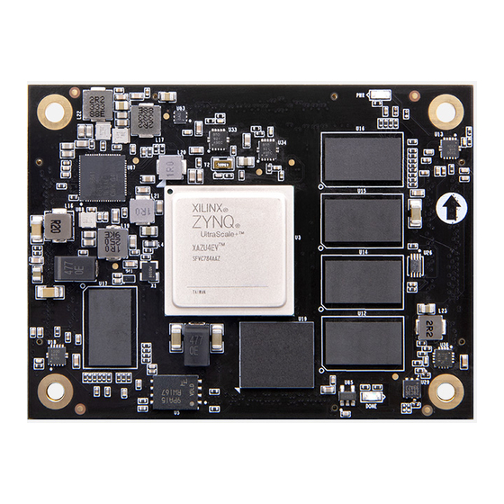
ZYNQ Ultrascale + FPGA Core Board ACU4EV User Manual Part 1: ACU4EV Core Board Introduction ACU4EV (core board model, the same below) FPGA core board, ZYNQ chip is based on XCZU4EV-1SFVC784I of XILINX company Zynq UltraScale+ MPSoCs EV Family. This core board uses 5 Micron DDR4 chips MT40A512M16GE, of which 4 DDR4 chips are mounted on the PS side to form a 64-bit data bus bandwidth and 4GB capacity. -
Page 5: Part 2: Zynq Chip
Figure 1-1: ACU4EV Core Board (Front View) Part 2: ZYNQ Chip The FPGA core board ACU4EV uses Xilinx's Zynq UltraScale+ MPSoCs EV family chip, module XCZU4EV-1SFVC784I. The PS system of the ZU4EV chip integrates 4 ARM Cortex™-A53 processors with a speed of up to 1.2Ghz and supports Level 2 Cache;... - Page 6 ZYNQ Ultrascale + FPGA Core Board ACU4EV User Manual Figure 2-1: Overall Block Diagram of the ZYNQ ZU4EV Chip The main parameters of the PS system part are as follows: ARM quad-core Cortex ™ -A53 processor, speed up to 1.5GHz, each...
-
Page 7: Part 3: Ddr4 Dram
SFVC784 Part 3: DDR4 DRAM The ACU4EV core board is equipped with 5 Micron (Micron) 1GB DDR4 chips, model MT40A512M16LY-062E, of which 4 DDR4 chips are mounted on the PS side to form a 64-bit data bus bandwidth and 4GB capacity. One DDR4... - Page 8 ZYNQ Ultrascale + FPGA Core Board ACU4EV User Manual of 1GB. The maximum operating speed of the DDR4 SDRAM on the PS side can reach 1200MHz (data rate 2400Mbps), and the 4 DDR4 storage systems are directly connected to the memory interface of the PS BANK504. The...
- Page 9 ZYNQ Ultrascale + FPGA Core Board ACU4EV User Manual The hardware connection of DDR4 SDRAM on the Pl Side is shown in Figure 3-2: Figure 3-2: DDR3 DRAM schematic diagram PS Side DDR4 DRAM pin assignment: Signal Name Pin Name...
- Page 10 ZYNQ Ultrascale + FPGA Core Board ACU4EV User Manual PS_DDR4_DQS6_N PS_DDR_DQS_N6_504 PS_DDR4_DQS7_P PS_DDR_DQS_P7_504 PS_DDR4_DQS7_N PS_DDR_DQS_N7_504 PS_DDR4_DQ0 PS_DDR_DQ0_504 AD21 PS_DDR4_DQ1 PS_DDR_DQ1_504 AE20 PS_DDR4_DQ2 PS_DDR_DQ2_504 AD20 PS_DDR4_DQ3 PS_DDR_DQ3_504 AF20 PS_DDR4_DQ4 PS_DDR_DQ4_504 AH21 PS_DDR4_DQ5 PS_DDR_DQ5_504 AH20 PS_DDR4_DQ6 PS_DDR_DQ6_504 AH19 PS_DDR4_DQ7 PS_DDR_DQ7_504 AG19 PS_DDR4_DQ8...
- Page 11 ZYNQ Ultrascale + FPGA Core Board ACU4EV User Manual PS_DDR4_DQ31 PS_DDR_DQ31_504 AC28 PS_DDR4_DQ32 PS_DDR_DQ32_504 PS_DDR4_DQ33 PS_DDR_DQ33_504 PS_DDR4_DQ34 PS_DDR_DQ34_504 PS_DDR4_DQ35 PS_DDR_DQ35_504 PS_DDR4_DQ36 PS_DDR_DQ36_504 PS_DDR4_DQ37 PS_DDR_DQ37_504 PS_DDR4_DQ38 PS_DDR_DQ38_504 PS_DDR4_DQ39 PS_DDR_DQ39_504 PS_DDR4_DQ40 PS_DDR_DQ40_504 PS_DDR4_DQ41 PS_DDR_DQ41_504 PS_DDR4_DQ42 PS_DDR_DQ42_504 PS_DDR4_DQ43 PS_DDR_DQ43_504 PS_DDR4_DQ44 PS_DDR_DQ44_504 PS_DDR4_DQ45 PS_DDR_DQ45_504...
- Page 12 ZYNQ Ultrascale + FPGA Core Board ACU4EV User Manual PS_DDR4_DM1 PS_DDR_DM1_504 AE23 PS_DDR4_DM2 PS_DDR_DM2_504 AE25 PS_DDR4_DM3 PS_DDR_DM3_504 AE28 PS_DDR4_DM4 PS_DDR_DM4_504 PS_DDR4_DM5 PS_DDR_DM5_504 PS_DDR4_DM6 PS_DDR_DM6_504 PS_DDR4_DM7 PS_DDR_DM7_504 PS_DDR4_A0 PS_DDR_A0_504 PS_DDR4_A1 PS_DDR_A1_504 PS_DDR4_A2 PS_DDR_A2_504 AB28 PS_DDR4_A3 PS_DDR_A3_504 AA28 PS_DDR4_A4 PS_DDR_A4_504 PS_DDR4_A5 PS_DDR_A5_504...
- Page 13 ZYNQ Ultrascale + FPGA Core Board ACU4EV User Manual PS_DDR4_CLK0_N PS_DDR_CK0_N_504 PS_DDR4_CKE0 PS_DDR_CKE0_504 PL Side DDR4 DRAM pin assignment: Signal Name Pin Name Pin Number PL_DDR4_DQS0_P IO_L22P_T3U_N6_DBC_AD0P_64 PL_DDR4_DQS0_N IO_L22N_T3U_N7_DBC_AD0N_64 PL_DDR4_DQS1_P IO_L16P_T2U_N6_QBC_AD3P_64 PL_DDR4_DQS1_N IO_L16N_T2U_N7_QBC_AD3N_64 PL_DDR4_DQ0 IO_L24N_T3U_N11_64 PL_DDR4_DQ1 IO_L24P_T3U_N10_64 PL_DDR4_DQ2 IO_L23N_T3U_N9_64 PL_DDR4_DQ3...
-
Page 14: Part 4: Qspi Flash
PL_DDR4_OTD IO_L19N_T3L_N1_DBC_AD9N_64 Part 4: QSPI Flash The FPGA core board ACU4EV is equipped with one 256MBit Quad-SPI FLASH chip to form an 8-bit bandwidth data bus, the flash model is MT25QU256ABA1EW9, which uses the 1.8V CMOS voltage standard. Due to the non-volatile nature of QSPI FLASH, it can be used as a boot device for the system to store the boot image of the system. -
Page 15: Part 5: Emmc Flash
PS_MIO5_500 AD16 Part 5: eMMC Flash The ACU4EV core board is equipped with a large-capacity 8GB eMMC FLASH chip, the model is MTFC8GAKAJCN-4M, it supports the HS-MMC interface of the JEDEC e-MMC V5.0 standard, and the level supports 1.8V or 3.3V. - Page 16 ZYNQ Ultrascale + FPGA Core Board ACU4EV User Manual as a large-capacity storage device in the ZYNQ system, such as storing ARM applications, system files and other user data files The specific models and related parameters of eMMC FLASH are shown in Table 5-1.
-
Page 17: Part 6: Clock Configuration
ZYNQ Ultrascale + FPGA Core Board ACU4EV User Manual MMC_DAT5 PS_MIO18_500 AC19 MMC_DAT6 PS_MIO19_500 AE19 MMC_DAT7 PS_MIO20_500 AD19 MMC_CMD PS_MIO21_500 AC21 MMC_CCLK PS_MIO22_500 AB20 MMC_RSTN PS_MIO23_500 AB18 Part 6: Clock Configuration The core board provides reference clock and RTC real-time clock for PS system and PL logic respectively, so that PS system and PL logic can work independently. - Page 18 ZYNQ Ultrascale + FPGA Core Board ACU4EV User Manual Figure 6-2: Passive Crystal Oscillator for RTC Clock pin assignment: Signal Name PS_PADI_503 PS_PADO_503 PS System Clock Source The X1 crystal on the core board provides a 33.333MHz clock input for the PS part.
-
Page 19: Part 7: Led
Part 7: LED There is a red power indicator (PWR) and a configuration LED (DONE) on the ACU4EV core board. When the core board is powered on, the power indicator will light up; after the FPGA configuration program, the configuration LED light will light up. -
Page 20: Part 8: Power Supply
Figure 7-1: LED Schematic in the Core Board Part 8: Power Supply The power supply voltage of the ACU4EV core board is DC12V, which is supplied by connecting the carrier board. The core board uses a PMIC chip TPS6508641 to generate all the power required by the XCZU4EV chip. For the TPS6508641 power supply design, please refer to the power supply chip manual. - Page 21 ZYNQ Ultrascale + FPGA Core Board ACU4EV User Manual In addition, the VCCIO power supply of BANK65 and BANK66 of XCZU4EV chip is provided by the carrier board, which is convenient for users to modify, but the maximum power supply cannot exceed 1.8V.
-
Page 22: Part 9: Acu4Ev Core Board Form Factors
ZYNQ Ultrascale + FPGA Core Board ACU4EV User Manual Part 9: ACU4EV Core Board Form Factors Figure 9-1: ACU4EV Core Board Form Factors Part Board Board Connectors Assignment The core board has a total of four high-speed expansion ports. It uses four 120-pin inter-board connectors (J29/J30/J31/J32) to connect to the carrier board. - Page 23 ZYNQ Ultrascale + FPGA Core Board ACU4EV User Manual level standard of BANK65 and BANK66 is determined by the VCCO_65 and VCCO_66 power supply of the carrier board, but cannot exceed +1.8V; the level standard of MIO is also 1.8V.
- Page 24 ZYNQ Ultrascale + FPGA Core Board ACU4EV User Manual B66_L3_P B65_L12_P B66_L3_N B65_L12_N B66_L1_P B65_L13_N B66_L1_N B65_L13_P B66_L6_P B65_L21_P B66_L6_N B65_L21_N B66_L16_P B65_L23_P B66_L16_N B65_L23_N B66_L15_P B66_L5_N B66_L15_N B66_L5_P B66_L4_P B66_L2_P B66_L4_N B66_L2_N B66_L11_P B66_L20_P B66_L11_N B66_L20_N B66_L12_P B66_L7_P B66_L12_N...
- Page 25 ZYNQ Ultrascale + FPGA Core Board ACU4EV User Manual B66_L14_N FPGA_TCK B66_L22_P FPGA_TDO B66_L22_N FPGA_TMS B66_L19_N B66_L21_N B66_L19_P B66_L21_P B66_L24_P B66_L17_P B66_L24_N B66_L17_N B66_L23_N B25_L9_P B66_L23_P B25_L9_N B25_L5_N B25_L10_P B25_L5_P B25_L10_N B66_L18_N B25_L12_P B66_L18_P B25_L12_N B25_L4_N B25_L11_P B25_L4_P B25_L11_N B26_L11_P...
- Page 26 ZYNQ Ultrascale + FPGA Core Board ACU4EV User Manual B26_L5_P B26_L4_P B26_L1_P B26_L12_P B26_L1_N B26_L12_N 505_CLK2_P 505_CLK1_P 505_CLK2_P 505_CLK1_P 505_CLK0_P 505_CLK3_P 505_CLK0_N 505_CLK3_N 505_TX3_P 505_TX1_P 505_TX3_N 505_TX1_N 505_RX3_P 505_TX0_P 505_RX3_N 505_TX0_N 505_TX2_P 505_RX1_P 505_TX2_N 505_RX1_N 505_RX2_P 505_RX0_P 505_RX2_N 505_RX0_N Pin assignment of board to board connector J31...
- Page 27 ZYNQ Ultrascale + FPGA Core Board ACU4EV User Manual B24_L1_P AE15 B44_L8_N AC11 B24_L1_N AE14 B44_L8_P AB11 B24_L12_P B24_L2_P AG14 B24_L12_N AA12 B24_L2_N AH14 B24_L3_P AG13 B24_L3_N AH13 B44_L12_N B44_L9_P AA11 B44_L12_P AB10 B44_L9_N AA10 B44_L10_N B44_L3_P AH12 B44_L10_P B44_L3_N...
- Page 28 ZYNQ Ultrascale + FPGA Core Board ACU4EV User Manual 224_CLK0_P 224_CLK1_P 224_CLK0_N 224_CLK1_N 224_RX3_P 224_TX3_P 224_RX3_N 224_TX3_N 224_RX2_P 224_TX2_P 224_RX2_N 224_TX2_N 224_RX1_P 224_TX1_P 224_RX1_N 224_TX1_N 224_RX0_P 224_TX0_P 224_RX0_N 224_TX0_N Pin assignment of board to board connector J32 J32 Pin Signal Name...
- Page 29 ZYNQ Ultrascale + FPGA Core Board ACU4EV User Manual PS_MIO76 PS_MIO60 PS_MIO61 PS_MIO39 PS_MIO62 PS_MIO38 PS_MIO63 PS_MIO65 PS_MIO40 PS_MIO66 PS_MIO44 PS_MIO67 PS_MIO45 PS_MIO68 PS_MIO47 PS_MIO64 PS_MIO48 PS_MIO69 PS_MIO41 PS_MIO74 PS_MIO32 PS_MIO73 PS_MIO46 PS_MIO72 PS_MIO50 PS_MIO71 PS_MIO49 PS_MIO75 PS_MIO34 PS_MIO70 PS_MIO26...
- Page 30 ZYNQ Ultrascale + FPGA Core Board ACU4EV User Manual +12V +12V +12V +12V +12V +12V +12V +12V +12V +12V +12V +12V +12V +12V Amazon Store: https://www.amazon.com/alinx 30 / 30 Sales Email: rachel.zhou@aithtech.com...
Need help?
Do you have a question about the ACU4EV and is the answer not in the manual?
Questions and answers