Table of Contents
Advertisement
Quick Links
Advertisement
Table of Contents

Related Manuals for Comtech EF Data PCB-4000A


Summary of Contents for Comtech EF Data PCB-4000A
- Page 1 PCB-4000A 1+1 Phase Combiner Installation and Operation Manual Part Number MN-PCB-4000A Revision 2 IMPORTANT NOTE: The information contained in this document supersedes all previously published information regarding this product. Product specifications are subject to change without prior notice.
- Page 2 PCB-4000A 1+1 Phase Combiner Revision 2 Copyright © 2018 Comtech EF Data. All rights reserved. Printed in the USA. Comtech EF Data, 2114 West 7th Street, Tempe, Arizona 85281 USA, 480.333.2200, FAX: 480.333.2161 Revision History Date Description 5-2017 Initial Release.
-
Page 3: Table Of Contents
Recommended Standard Designations ..................... ii Metric Conversion ............................ii Safety and Compliance ..........................iii Electrical Safety Notice ..........................iii Product Support ............................iv Comtech EF Data Headquarters ....................... iv Warranty Policy ............................v Limitations of Warranty ..........................v Exclusive Remedies ..........................vi CHAPTER 1. - Page 4 PCB-4000A 1+1 Phase Combiner Revision 2 3.2.3 System Component Installation and Interconnection ............... 3–4 3.2.4 LED Status Operation ....................... 3–6 Initial System Setup and Verification ..................3–8 Gain or Amplitude Balance Verification and Alignment ............3–9 Amplitude Alignment (as necessary) ..................3–10 Phase Alignment ........................
-
Page 5: Table Of Contents
PCB-4000A 1+1 Phase Combiner Revision 2 A.3.1 HPOD 1:1 Redundancy Pole Mount Kit (PL/12319-1)............A–13 A.3.2 1:2 Redundant HPOD Mounting Kit (KT-0000017) ..............A–15 A.3.3 Uni-Strut Mount HPOD Mounting Bracket Kit (KT/12300-1) ........... A–17 A.3.4 Vertical Frame Uni-Strut Mount HPOD Mounting Bracket Kit (KT-0021261) ......A–19... - Page 6 Figure 1-3. Combining Loss vs. Phase Imbalance Summary of Specifications........1–4 Figure 1-4. PCB-4000A Dimensional Envelope ..................1–6 Figure 3-1. PCB-4000A 1+1 Phase Combiner System Assembly Example ..........3–2 Figure 3-2. PCB-4000A External Connectors - Front ................3–3 Figure 3-3. PCB-4000A External Connectors – Right Side ..............3–3 Figure 3-4.
- Page 7 PCB-4000A 1+1 Phase Combiner Revision 2 LIST OF TABLES Table 2-1. External Connectors ......................... 2–1 Table 2-2. Connector J1 Pinouts ....................... 2–2 Table 2-3. Connectors J2 and J3 Pinouts ....................2–3 Table 2-4. Connector J5 Pinouts ....................... 2–4 Table 2-5. Connector J6 Pinouts ....................... 2–5 Table 3-1.
- Page 8 PCB-4000A 1+1 Phase Combiner Revision 2 Acronym List Acronym Description Amplitude Offset Electronic Industries Association Ground HPOD High Powered Outdoor Amplifier Light Emitting Diode M&C Monitor and Control Network Management System Object Identifiers Printed Circuit Board PCCB Phase Combiner Control Box...
-
Page 9: Preface
1+1 Phase Combiner. This is an informational document intended for the persons responsible for the operation and maintenance of the PCB-4000A. Comtech EF Data has reviewed this manual thoroughly in order to provide an easy-to-use guide to your equipment. All statements, technical information, and recommendations in this manual... -
Page 10: Warnings, Cautions, And Notes
A NOTE: gives you important information about a task or the equipment. A REFERENCE directs you to important operational information or details furnished elsewhere, either in the manual or in adjunct Comtech EF Data publications. Examples of Multi-Hazard Notices... -
Page 11: Safety And Compliance
Double pole / neutral fusing is used on the prime power supply input. This equipment is designed to minimize exposure of personnel to hazards. For further information, contact the Comtech EF Data Customer Support Department. The persons responsible for the operation and maintenance of the PCB-4000A must: •... -
Page 12: Product Support
PCB-4000A 1+1 Phase Combiner Revision 2 Product Support For all product support, please call: +1.240.243.1880 +1.866.472.3963 (toll free USA) By email: techsupport@comtechefdata.com Comtech EF Data Headquarters http://www.comtechefdata.com Comtech EF Data Corp. 2114 West 7th Street Tempe, Arizona USA 85281 +1.480.333.2200... -
Page 13: Warranty Policy
Comtech EF Data Corporation, would affect the reliability or detracts from the performance of any part of the product, or is damaged as the result of use in a way or with equipment that had not been previously approved by Comtech EF Data Corporation. -
Page 14: Exclusive Remedies
The buyer shall pass on to any purchaser, lessee, or other user of Comtech EF Data Corporation’s products, the aforementioned warranty, and shall indemnify and hold harmless Comtech EF Data... -
Page 15: Chapter 1. Introduction
Solid State Power Amplifiers (SSPAs), form a complete 1+1 phase combined system that doubles the available output power. The PCB-4000A also features a “soft fail” configuration; i.e., if one SSPA experiences a failure, the total output power will be reduced by only 3 dB, rather than 6 dB. -
Page 16: Functional Description
Revision 2 Functional Description The PCB-4000A is available in a C-Band version. Contact Comtech EF Data for X-band and Ku- band versions. The box may be included in a top-level system assembly or as a subassembly kit. For application examples, see Appendix A. ASSEMBLY KITS. - Page 17 PCB-4000A 1+1 Phase Combiner Revision 2 The block diagrams shown in Figure 1-2 depict the major components of the 1:1 phase combined system. (These diagrams employ High Powered Outdoor Amplifiers (HPODs) as the designated SSPAs.) The Phase Combiner Control Box (PCCB) contains a microprocessor-based Monitor and Control (M&C) circuit board to control the system.
-
Page 18: Theory Of Operation
Naturally, two separate amplifiers are likely to have different phase and gain characteristics. The PCB-4000A 1+1 system is designed such that the phase difference between the two amplifier paths is compensated by adjusting the phase shifter in the PCCB. This is done at the factory for the full amplifier bandwidth, and should not normally require further adjustment in the field unless an amplifier has been replaced. -
Page 19: System Gain
1.3.4 Soft Fail Protection In the event of a failure of one of the SSPAs, the PCB-4000A controls the waveguide switches such that the good unit’s power is routed around the “Magic-Tee” combiner directly to the output port. This results in only a 3 dB power loss, or “soft failure”. Without the waveguide switches, a failure in one unit would result in a 6 dB power loss. -
Page 20: Dimensional Envelope
PCB-4000A 1+1 Phase Combiner Revision 2 Dimensional Envelope All dimensions are in English units; metric units are shown in parentheses. This figure is typical for the C-Band versions of the PCB-4000A. Figure 1-4. PCB-4000A Dimensional Envelope Introduction 1–6 MN-PCB-4000A... -
Page 21: Chapter 2. External Connectors
M&C. This chapter summarizes the connectors provided for all necessary external connections between the PCB-4000A and other equipment. Table 2-1 lists the external connectors grouped according to service function. Refer to Figure 3-2 for External Connectors illustration. Table 2-1. External Connectors... -
Page 22: Monitor And Control (M&C) Interface Connectors
PCB-4000A 1+1 Phase Combiner Revision 2 Monitor and Control (M&C) Interface Connectors All M&C connectors are found on the front panel of the PCCB box. 2.2.1 SYSTEM COM | J1 Connector The 19-pin circular SYSTEM COM | J1 connector, type MS3112E14-19S, serves as the primary input between the user and the PCCB for controlling and monitoring both SSPAs. -
Page 23: Sspa Com 1 | J2 And Sspa Com 2 | J3 Connectors
PCB-4000A 1+1 Phase Combiner Revision 2 2.2.2 SSPA COM 1 | J2 and SSPA COM 2 | J3 Connectors The 19-pin circular SSPA COM 1 | J2 and SSPA COM 2 | J3 connectors, type MS3112E14-19S, serve as the primary input/output interfaces between the PCCB and its specified SSPA. -
Page 24: Sspa Sw Out | J5 Connector
PCB-4000A 1+1 Phase Combiner Revision 2 SSPA SW OUT | J5 Connector The 19-pin circular SSPA SW OUT | J5 connector, type MS3112E14-19S, connects via a “Y” cable to the SSPA #1 and SSPA #2 waveguide switches. The typical pinout specification is provided in Table 2-4. -
Page 25: Rf Input Switch | J6 Connector
PCB-4000A 1+1 Phase Combiner Revision 2 2.3.1 RF INPUT SWITCH | J6 Connector The PCCB contains a built-in selector switch – a latching 28 VDC coaxial unit. The switch position is selected by the 6-pin circular RF INPUT SWITCH | J6 connector (P/N CN/MS-PT07M6PC). Its pinout specification is provided in Table 2-5. -
Page 26: Rf Interface Connectors
PCB-4000A 1+1 Phase Combiner Revision 2 RF Interface Connectors 2.4.1 RF IN 1 | J7 and RF IN 2 | J8 Connectors The Type ‘N’ RF IN 1 | J7 and RF IN 2 | J8 connectors serve as RF signal input interfaces to the PCCB. Note that: •... -
Page 27: Power And Ground Interfaces
2.5.1 AC Power The PCB-4000A derives its power from the SSPAs. Each SSPA provides a +24V signal line via cables interconnecting the SSPAs to the SSPA COM 1 | J2 and SSPA COM 2 | J3 connectors (Pin ‘R’ – see Table 2-3). These two signals are “diode OR’ed” to provide redundancy. - Page 28 PCB-4000A 1+1 Phase Combiner Revision 2 Notes: External Connectors 2–8 MN-PCB-4000A...
-
Page 29: Chapter 3. Operation And Adjustment Procedures
However, if an amplifier or other critical system component is replaced (e.g., the PCB-4000A unit), the procedures provided in this chapter explain the steps necessary to restore proper system operation. -
Page 30: System Assembly, Cabling Connections, And Installation
3.2.1 1+1 Phase Combiner System Assembly Figure 3-1 shows an example of the PCB-4000A deployed in a typical 1+1 phase combined system (see Appendix A. ASSEMBLY KITS for details on band-specific system applications). Figure 3-1. PCB-4000A 1+1 Phase Combiner System Assembly Example Operation and Adjustment Procedures 3–2... -
Page 31: Pccb Cabling Connections
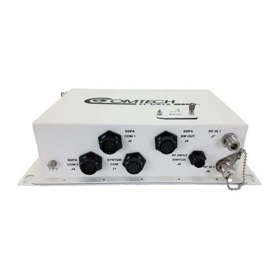
PCB-4000A 1+1 Phase Combiner Revision 2 3.2.2 PCCB Cabling Connections Figure 3-2. PCB-4000A External Connectors - Front Figure 3-3. PCB-4000A External Connectors – Right Side Operation and Adjustment Procedures 3–3 MN-PCB-4000A... -
Page 32: System Component Installation And Interconnection
It may be necessary to slightly adjust each SSPA to prevent undue stress on the waveguide structure. Tighten all hardware when proper alignment is achieved. Assemble the PCB-4000A PCCB to the mounting structure. Install the Type ‘N’ RF Phase Matched Coaxial Cables (CEFD P/N CA/RF11872-1). Each cable is labeled according to its destination SSPA: Connect the cable labeled “SSPA1”... - Page 33 PCB-4000A 1+1 Phase Combiner Revision 2 Step Procedure Install the “COM” Cable (CEFD P/N CA/WR11966-2) between each of the following PCCB connectors and their corresponding SSPA “COM” ports: (PCCB) “SSPA COM 1 | J2” to SSPA #1 • (PCCB) “SSPA COM 2 | J3” to SSPA #2 •...
-
Page 34: Led Status Operation
Each LED provides visual cues to the operational, online, and offline status of the system. Figure 3-5 illustrates the location of the LED indicators. Located on the top of the PCB-4000A enclosure under a pivoting protective plate, view the LEDs by first loosening the captive screw that keeps the plate in place, and then swiveling the plate to reveal the LED display window. -
Page 35: Table 3-1. Led Descriptions
PCB-4000A 1+1 Phase Combiner Revision 2 The behavior of the LEDs, as they appear under varying operational conditions, is as follows: Table 3-1. LED Descriptions LED * Color / Behavior Description Green Phase Combiner has no summary fault. (LED 1) A Summary Fault has occurred. -
Page 36: Initial System Setup And Verification
PCB-4000A 1+1 Phase Combiner Revision 2 Initial System Setup and Verification Verify that the system has been assembled, that all cables have been connected, and that the output port is terminated in a broadband high power load as depicted in Figure 1-2 block diagram in Chapter 1. -
Page 37: Gain Or Amplitude Balance Verification And Alignment
PCB-4000A 1+1 Phase Combiner Revision 2 Gain or Amplitude Balance Verification and Alignment This procedure is generally not necessary if all parameters of Section 3.3 have been met. As a result of the configuration of the waveguide switches in a 1+1 system, it is possible to measure the individual gain of each SSPA path by switching each SSPA individually to the output load. -
Page 38: Amplitude Alignment (As Necessary)
PCB-4000A 1+1 Phase Combiner Revision 2 Amplitude Alignment (as necessary) Even if the difference of each individual SSPA path is greater than ±1 dB, amplitude adjustment may not be necessary to meet all parameters of Section 0. However, if these parameters have not been met, then fine tuning adjustment is advisable. -
Page 39: Phase Alignment
PCB-4000A 1+1 Phase Combiner Revision 2 Phase Alignment As the system is aligned at the factory, this step is typically not required unless it is necessary to replace one of the SSPAs or other critical path components. Make sure to meet all parameters of Section 0 before performing this adjustment. -
Page 40: System Online And Transmitting
PCB-4000A 1+1 Phase Combiner Revision 2 System Online and Transmitting This procedure assumes that the system installation is complete and that access to the system output port is unavailable due to current system traffic. To check for proper operation, measure and compare the difference in power transmitted versus the power dissipated in the load termination. -
Page 41: Chapter 4. Updating Firmware
Revision 2 Chapter 4. UPDATING FIRMWARE Update Firmware via the Internet To ensure optimal performance, it is important to operate the PCB-4000A with its latest available firmware. The PCB-4000A 1+1 Phase Combiner is factory-shipped with the latest version of operating firmware. -
Page 42: Ethernet Ftp Upload Procedure
CEFD Customer Support for ordering information. Figure 4-1. Typical Unit to PC Connection a. Connect the user PC serial port to the PCB-4000A “SYSTEM COM | J1” port. b. On the PC: Open the terminal emulator program. Refer to your terminal emulator program HELP feature or user guide for operating and configuration instructions. -
Page 43: Figure 4-2. Temporary Folder Setup Using Windows Desktop
On the PC: Via serial remote control, obtain the firmware number by using the <1/FRW? query. See Chapter 5. SERIAL REMOTE CONTROL for information and instructions on using remote commands and queries via the PCB-4000A Serial Interface. 4. Create a temporary folder (subdirectory) on the user PC for the firmware archive download. -
Page 44: Figure 4-3. Temporary Folder Setup Using Windows Explorer
PCB-4000A 1+1 Phase Combiner Revision 2 b. Use Windows Explorer to create and rename the temporary folder. • Select File > New > Folder to create the temporary folder. The new folder will be created in the active folder. •... -
Page 45: Figure 4-5. Temporary Folder Setup Using Windows Command Line
PCB-4000A 1+1 Phase Combiner Revision 2 d. Use Windows Command-line to create the temporary folder. • First, click [Start] on the Windows taskbar, and then click the ‘Run...’ icon (or, depending on Windows OS versions prior to Windows 95, click the ‘MS-DOS Prompt’... -
Page 46: Download And Extract The Firmware Update
Revision 2 Download and Extract the Firmware Update 1. First, download the firmware update file from the Comtech EF Data Web site: a. Go online to www.comtechefdata.com. b. On the Main page – under Support Information or the Support tab, select the Software Downloads hyperlink. -
Page 47: Figure 4-6. Download Firmware Archive File
Command-line. • Type “dir” to list the files extracted to the temporary directory from the downloaded archive file. The firmware files have been successfully downloaded and are now available for transfer to the PCB-4000A. Updating Firmware 4–7 MN-PCB-4000A... -
Page 48: Firmware Upgrade
RED (faulted) to indicate the current status of the PCCB, SSPA1, and SSPA2 operations. See Chapter 3. OPERATION and ADJUSTMENT PROCEDURES, Section 3.2.4, for additional information on the LED operation states. The PCB-4000A Firmware Update Process is now complete. Updating Firmware 4–8... -
Page 49: Chapter 5. Serial Remote Control
Overview Remote monitor and control of the PCB-4000A 1+1 Phase Combiner is available only through an EIA-232 connection, and data is transmitted in asynchronous serial form using ASCII characters. Control and status information is transmitted in packets of variable length, in accordance with the structure and protocol defined in later sections. -
Page 50: Remote Commands And Queries Ovierview
PCB-4000A 1+1 Phase Combiner Revision 2 Remote Commands and Queries Ovierview 5.2.1 Basic Protocol All data is transmitted as asynchronous serial characters, suitable for transmission and reception by a UART. The asynchronous character is fixed at 8-N-1 (8 data bits, no parity, one stop bit). Only two baud rates are supported: 9600 baud and 19200 baud. -
Page 51: Packet Structure
PCB-4000A 1+1 Phase Combiner Revision 2 5.2.2 Packet Structure Controller-to-Target Start of Packet Target Address Address Delimiter Instruction Code Code Qualifier Optional Arguments End of Packet < = or ? Carriage Return ASCII code 60 ASCII code 47 ASCII codes 61 or 63... -
Page 52: 5.2.2.2 Target (Base) Address
PCB-4000A 1+1 Phase Combiner Revision 2 5.2.2.2 Target (Base) Address Up to 9,999 devices can be uniquely addressed. In the EIA-232 application, the permissible range of values is 1 to 9999. It is programmed into a Target unit using serial remote control. The factory default target address is 1. -
Page 53: 5.2.2.4 Address Delimiter
PCB-4000A 1+1 Phase Combiner Revision 2 5.2.2.4 Address Delimiter This is the “forward slash” character '/' (ASCII code 47). 5.2.2.5 Instruction Code This three-character alphabetic sequence identifies the subject of the message. Wherever possible, the instruction codes have been chosen to have some significance. This aids in the readability of the message if seen in its raw ASCII form. Upper and lower case alphabetic characters (i.e., A-Z [ASCII codes 65-90], and a-z [ASCII codes 97-122]) may be used. -
Page 54: Optional Message Arguments
PCB-4000A 1+1 Phase Combiner Revision 2 Symbol Definition The ? code is only used as follows: (ASCII code 63) If the Controller sends an instruction to set a parameter to a particular value, then, if the value sent in the argument is not valid, the Target will acknowledge the message by replying (for example) with MUT? (with no message arguments). -
Page 55: Remote Commands / Queries
PCB-4000A 1+1 Phase Combiner Revision 2 Remote Commands / Queries Index Notes: Column ‘C’ = Command; Column ‘Q’ = Query; columns marked ‘X’ designate instruction code as Command only, Query only, or Command/Query. CODE PAGE CODE PAGE CODE PAGE CODE PAGE 5–8... - Page 56 PCB-4000A 1+1 Phase Combiner Revision 2 Command Command Arguments for Response to Query Response to Description of Arguments Query Valid Parameter Command Query (Instruction Valid for Command or (Instruction for PCB or (Note that all arguments are ASCII numeric codes – i.e.,...
- Page 57 PCB-4000A 1+1 Phase Combiner Revision 2 Command Command Arguments for Response to Query Response to Description of Arguments Query Valid Parameter Command Query (Instruction Valid for Command or (Instruction for PCB or (Note that all arguments are ASCII numeric codes – i.e.,...
- Page 58 PCB-4000A 1+1 Phase Combiner Revision 2 Command Command Arguments for Response to Query Response to Description of Arguments Query Valid Parameter Command Query (Instruction Valid for Command or (Instruction for PCB or (Note that all arguments are ASCII numeric codes – i.e.,...
- Page 59 PCB-4000A 1+1 Phase Combiner Revision 2 Command Command Arguments for Response to Query Response to Description of Arguments Query Valid Parameter Command Query (Instruction Valid for Command or (Instruction for PCB or (Note that all arguments are ASCII numeric codes – i.e.,...
- Page 60 Equipment alphanumeric The unit returns a string indicating the Model Number and the (see Type value of internal software revision installed. Description of Arguments for Example: PCB-4000A Phase Combiner Ver: 1.1.1 details) Retrieve 42 bytes, Query only. RMS? RMS=x….x alphanumeric Maintenance Used to Query the maintenance status of the unit.
- Page 61 PCB-4000A 1+1 Phase Combiner Revision 2 Command Command Arguments for Response to Query Response to Description of Arguments Query Valid Parameter Command Query (Instruction Valid for Command or (Instruction for PCB or (Note that all arguments are ASCII numeric codes – i.e.,...
- Page 62 PCB-4000A 1+1 Phase Combiner Revision 2 Command Command Arguments for Response to Query Response to Description of Arguments Query Valid Parameter Command Query (Instruction Valid for Command or (Instruction for PCB or (Note that all arguments are ASCII numeric codes – i.e.,...
- Page 63 PCB-4000A 1+1 Phase Combiner Revision 2 Command Command Arguments for Response to Query Response to Description of Arguments Query Valid Parameter Command Query (Instruction Valid for Command or (Instruction for PCB or (Note that all arguments are ASCII numeric codes – i.e.,...
- Page 64 PCB-4000A 1+1 Phase Combiner Revision 2 Command Command Arguments for Response to Query Response to Description of Arguments Query Valid Parameter Command Query (Instruction Valid for Command or (Instruction for PCB or (Note that all arguments are ASCII numeric codes – i.e.,...
-
Page 65: Chapter 6. Ethernet-Based Remote Product Management
The PCB-4000A is operating with the latest version firmware files. • The PCB-4000A is connected to a user-supplied, Windows-based PC, and: The PC Ethernet port is connected to the PCB-4000A SYSTEM COM | J1 connector. Ethernet Management Interface Protocols The user PC facilitates access to Ethernet-based remote monitor and control (M&C) of the PCB-4000A through the Simple Network Management Protocol (SNMP). -
Page 66: 6.3.1 Management Information Base (Mib) Files
The Read and Write Community Strings can be configured using serial remote command RCM and WCM when remote state is at Serial Remote. For proper SNMP operation, the PCB-4000A MIB files must be used with the associated version of the unit. Refer to the PCB-4000A FW Release Notes for information on the required FW/SW compatibility. -
Page 67: Appendix A. Assembly Kits
4000A 1+1 Phase Combined System – an example is shown as Figure A-1. The PCB-4000A 1+1 Phase Combiner stand alone unit is available in a C-Band version only. Contact Comtech EF Data for X-Band or Ku-Band versions. The PCCB may be available as a top assembly line item or as a kit subassembly item. -
Page 68: Figure A-1. Pcb-4000A 1+1 Phase Combined System
PCB-4000A 1+1 Phase Combiner Revision 2 Figure A-1. PCB-4000A 1+1 Phase Combined System Assembly Kits A–2 MN-PCB-4000A... -
Page 69: Summary Of Available Assemblies
Summary of Available Assemblies Table A-1 outlines availability of assembly kits for the PCB-4000A. This includes common subassemblies that may be shared amongst the available configurations. Note that since the model of the SSPA pair deployed within a 1+1 Phase Combined System may vary, the illustrations provided herein either show installed SSPAs for reference purposes only, or otherwise intentionally omit the depiction of any installed SSPA. - Page 70 PCB-4000A 1+1 Phase Combiner Revision 2 BLANK PAGE Assembly Kits A–4 MN-PCB-4000A...
-
Page 71: C-Band Unit Assemblies
PCB-4000A 1+1 Phase Combiner Revision 2 C-Band Unit Assemblies A.2.1 C-Band 1+1 Phase Combined HPOD Top Assembly Kit (KT-0000055) Figure A-2. C-Band 1+1 Phase Combined HPOD Top Assembly Kit (KT-0000055) Assembly Kits A–5 MN-PCB-4000A... -
Page 72: Table A-2. C-Band 1+1 Phase Combined Hpod Top Assembly Kit - Bom (Kt-0000055
PCB-4000A 1+1 Phase Combiner Revision 2 Table A-2. C-Band 1+1 Phase Combined HPOD Top Assembly Kit - BOM (KT-0000055) Figure A-2 Item CEFD Part No. Description KT-0000017 1:2 Unistrut Mounting Kit KT/12300-1 HPOD Mounting Bracket Kit KT-0021171 C-Band Phase Combiner Box and Bracket Kit... -
Page 73: Phase Combiner Box And Bracket Kit (Kt-0021171
PCB-4000A 1+1 Phase Combiner Revision 2 A.2.2 Phase Combiner Box and Bracket Kit (KT-0021171) Figure A-3. Phase Combiner Box and Bracket Kit (KT-0021171) Assembly Kits A–7 MN-PCB-4000A... -
Page 74: Table A-3. Phase Combiner Box And Bracket Kit - Bom (Kt-0021171
PCB-4000A 1+1 Phase Combiner Revision 2 Table A-3. Phase Combiner Box and Bracket Kit – BOM (KT-0021171) See Figure A-3 Item CEFD Part No. Description FP-0022138 Bracket, HPOD Phase Combiner HW/1/4-20HEXNUT 1/4-20 HEXNUT,SS HW/1/4-20X1SHCS 1/4X20X1 Socket HD Cap Screws HW/1/4-FLT... -
Page 75: C-Band 1:1 Phase Combined Waveguide And Switches, Hpod (Kt-0000054
PCB-4000A 1+1 Phase Combiner Revision 2 A.2.3 C-Band 1:1 Phase Combined Waveguide and Switches, HPOD (KT-0000054) Figure A-4. C-Band 1:1 Phase Combined Waveguide and Switches, HPOD (KT-0000054) Assembly Kits A–9 MN-PCB-4000A... -
Page 76: Table A-4. C-Band 1:1 Phase Combined Waveguide And Switches, Hpod - Bom (Kt-0000054
PCB-4000A 1+1 Phase Combiner Revision 2 Table A-4. C-Band 1:1 Phase Combined Waveguide and Switches, HPOD - BOM (KT-0000054) See Figure A-4 Item CEFD Part No. Description FP-0000414 MOUNTING BRACKET, DUAL VERTICAL SWITCHES, CPR-137 HW/3/8SPRINGNUT SPRINGNUT, 3/8-16, SHORT SPRING, SS (P3300) -
Page 77: Vertical Mounting Frame Kit (Kt-0021179
PCB-4000A 1+1 Phase Combiner Revision 2 A.2.4 Vertical Mounting Frame Kit (KT-0021179) Figure A-5. Vertical Mounting Frame Kit (KT-0021179) Assembly Kits A–11 MN-PCB-4000A... -
Page 78: Table A-5. Vertical Mounting Frame Kit - Bom (Kt-0021179
PCB-4000A 1+1 Phase Combiner Revision 2 Table A-5. Vertical Mounting Frame Kit – BOM (KT-0021179) See Figure A-5 Item CEFD Part No. Description KT-0021175 MOUNTING KIT, 1:2 REDUNDANT HPOD, INDOOR MTG FRAME, VERTICAL WITH POST BASES KT-0021261 MOUNTING BRACKET KIT, UNI STRUT MOUNT HPOD... -
Page 79: Common Kit Subassemblies
PCB-4000A 1+1 Phase Combiner Revision 2 Common Kit Subassemblies A.3.1 HPOD 1:1 Redundancy Pole Mount Kit (PL/12319-1) Figure A-6. HPOD 1:1 Redundancy Pole Mount Kit (PL/12319-1) Assembly Kits A–13 MN-PCB-4000A... -
Page 80: Table A-6. Hpod 1:1 Redundancy Pole Mount Kit - Bom (Pl/12319-1
PCB-4000A 1+1 Phase Combiner Revision 2 Table A-6. HPOD 1:1 Redundancy Pole Mount Kit - BOM (PL/12319-1) See Figure A-6 Item CEFD Part No. Description Strut (Shown for reference only) Bracket, Strap Tensioner FP/BR0072 Strap, Termination, Pole Mounting Kit FP/BR0070... -
Page 81: 1:2 Redundant Hpod Mounting Kit (Kt-0000017
PCB-4000A 1+1 Phase Combiner Revision 2 A.3.2 1:2 Redundant HPOD Mounting Kit (KT-0000017) Figure A-7. 1:2 Redundant HPOD Mounting Kit (KT-0000017) Assembly Kits A–15 MN-PCB-4000A... -
Page 82: Table A-8. 1:2 Redundant Hpod Mounting Kit - Bom (Kt-0000017
PCB-4000A 1+1 Phase Combiner Revision 2 Table A-8. 1:2 Redundant HPOD Mounting Kit - BOM (KT-0000017) See Figure A-7 Item No. CEFD Part No. Description FP-0000134 Unistrut, Dual Channel, 74.13” LG FP/BR11932-1 Bracket, Unistrut, SS, 26.25” LG HW/3/8SPRINGNUT Spring Nut, 3/8-16, Short Spring, SS (P3300) -
Page 83: Uni-Strut Mount Hpod Mounting Bracket Kit (Kt/12300-1
PCB-4000A 1+1 Phase Combiner Revision 2 A.3.3 Uni-Strut Mount HPOD Mounting Bracket Kit (KT/12300-1) Figure A-8. Uni-Strut Mount HPOD Mounting Bracket Kit (KT/12300-1) Assembly Kits A–17 MN-PCB-4000A... -
Page 84: Table A-9. Uni-Strut Mount Hpod Mounting Bracket Kit - Bom (Kt/12300-1
PCB-4000A 1+1 Phase Combiner Revision 2 Table A-9. Uni-Strut Mount HPOD Mounting Bracket Kit - BOM (KT/12300-1) See Figure A-8 Item CEFD Part No. Description FP/BR12239-1 Bracket, Unistrut HW/3/8SPRINGNUT Spring Nut, 3/8-16, Short Spring, SS (P3300) HW/3/8-FLT Washer, Flat, 3/8... -
Page 85: Vertical Frame Uni-Strut Mount Hpod Mounting Bracket Kit (Kt-0021261
PCB-4000A 1+1 Phase Combiner Revision 2 A.3.4 Vertical Frame Uni-Strut Mount HPOD Mounting Bracket Kit (KT-0021261) Figure A-9. Vertical Frame Uni-Strut Mount HPOD Mounting Bracket Kit (KT-0021261) Assembly Kits A–19 MN-PCB-4000A... -
Page 86: Table A-10. Vertical Frame Uni-Strut Mount Hpod Mounting Bracket Kit (Kt-0021261
PCB-4000A 1+1 Phase Combiner Revision 2 Table A-10. Vertical Frame Uni-Strut Mount HPOD Mounting Bracket Kit (KT-0021261) See Figure A-9 Item CEFD Part No. Description FP-0022325 Mounting Bracket, HPOD & LPOD PS-2, with Gussets HW/3/8SPRINGNUT Spring Nut, 3/8-16, Short Spring, SS (P3300 Channel) HW/3/8-16X1BLT Bolt, Hex Head, 3/8-16 x 1”... - Page 88 2114 85281 WEST TH STREET TEMPE ARIZONA 480 • 333 • 2200 PHONE 480 • 333 • 2161...
Need help?
Do you have a question about the PCB-4000A and is the answer not in the manual?
Questions and answers