Table of Contents

Related Manuals for JVC GY-DV5000U


Summary of Contents for JVC GY-DV5000U
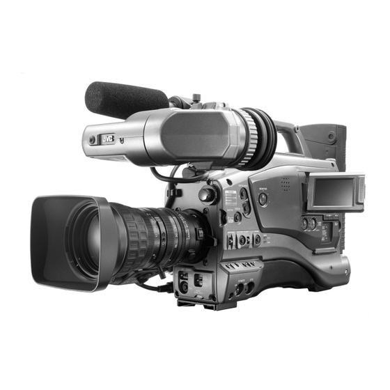
- Page 1 SERVICE MANUAL DV CAMCORDER GY-DV5000U/GY-DV5000E The photo shows the GY-DV500 DV camcorder with an optional lens, viewfinder,microphone and mic holder. No. 60148 November 2002 100% recycled paper COPYRIGHT © 2002 VICTOR COMPANY OF JAPAN, LTD.
-
Page 2: Table Of Contents
TABLE OF CONTENTS Section Title Page Section Title Page Important Safety Precautions SECTION 4 CHARTS AND DIAGRAMS INSTRUCTIONS 4.1 INDEX TO PAGES OF MAIN BOARDS AND CIRCUIT BOARD LOCATION ........... 4-3 SECTION 1 SERVICE CAUTIONS AND DISASSEMBLY 4.1.1 Circuit board location ............4-3 1.1 RESETTING THE POWER CIRCUIT PROTECTION BREAKER . -
Page 3: Important Safety Precautions
Important Safety Precautions Prior to shipment from the factory, JVC products are strictly inspected to conform with the recognized product safety and electrical codes of the countries in which they are to be sold. However, in order to maintain such compliance, it is equally important to implement the following precautions when a set is being serviced. - Page 4 Safety Check after Servicing Examine the area surrounding the repaired location for damage or deterioration. Observe that screws, parts and wires have been returned to original positions, Afterwards, perform the following tests and confirm the specified values in order to verify compli- ance with safety standards.
-
Page 5: Resetting The Power Circuit Protection Breaker
SECTION 1 SERVICE CAUTIONS AND DUSASSEMBLY RESETTING THE POWER CIRCUIT PROTECTION 1.2.2 Opening the Right side cover BREAKER (1) Loosen the 4 screws This unit employs a power circuit protection breaker in place a fuse to disconnect from the main power and to thus protect the internal circuitry from damage caused by any current overload. -
Page 6: Layouts The Major Boards
LAYOUTS THE MAJOR BOARDS PSIF XLRF Fig. 1-3-1 Fig. 1-3-2 TGDF MECHA MDA/DC DBCP MRELAY Fig. 1-3-3 XLRR PJUNC DV/CPU Fig. 1-3-4 Fig. 1-3-5... -
Page 7: Removing The Optical Block Assembly And The Optical Filter Assembly
REMOVING THE OPTICAL BLOCK ASSEMBLY AND (4) Remove the 4 screws , then remove the TGDF board and THE OPTICAL FILTER ASSEMBLY mounting bracket. (1) Remove the right side cover (see section 1.2.2). (2) Remove the 4 screws Fig.1-4-3 (5) Flip open CN1,CN2 and CN3 and unplug the FFC cable. Fig. -
Page 8: Removing Major Boards From The Camera
(7) Removing the 4 screws and separate the optical block 1.5 REMOVING MAJOR BOARDS FROM THE CAMERA assembly from the front panel. 1.5.1 Removing the TGDF board. (1) Remove the optical block assembly together with TGDF front panel. (see section 1.4) (2) Remove the 4 screws . -
Page 9: Removing The Dbcp Board
1.5.2 Removing the DBCP board REMOVING THE LCD MONITOR (1) Open the right side cover (see section 1.2.2). (1) Open the right side cover (see section 1.2.2). And remove (2) Remove the 2 screws , Now the DBCP board can be the each wire assembly and FFC cable from ALS board side. -
Page 10: Removing The Vcr Unit
(6) TURN the LCD monitor screen so that the face upward, and REMOVING THE VCR UNIT push it toward the inner side of the right side cover as shown (1) Remove the left side cover (see section1.2.1) in figure. (2) Remove the 4 screws fixed on VCR unit. -
Page 11: Removing The Battery Case And If Board
(5) If it will be required to repair or maintenance at the VCR unit (3) Remove the 3 screws . Now the IF board can be removed. which is removed, refer to the section 2. Fig.1-7-4 Fig.1-8-2 REMOVING THE BATTERY CASE AND IF BOARD 1.9 SERVICE MENUS ASSEMBLY 1.9.1 Modes required in servicing... -
Page 12: Operation In The First-Level Of The Service Menu
1.9.2 Operation in the first-level of the service menu 1.9.3 CAMERA 1 menu (1) While holding down the specified button(s) (FAS, LOLUX), (1) In a service menu, place the cursor ( 3) on “CAMERA 1” press and hole the MENU button for more than 1 second. and push the SHUTTER dial to display the CAMERA1 menu. -
Page 13: Camera 2 Menu
White blemish detection Details on correctable white blemish Move the cursor at the item "ERROR DETECT CANCEL" and Up to 32 errors with composite video levels of 50mV or more select "EXECUTE", then push the SHUTTER dial then CCD can be corrected. However, the maximum number of errors white blemish detect operation start automaticaly. -
Page 14: Camera 3 Menu
1.9.5 CAMERA 3 menu 1.9.7 VTR 2 menu In a service menu, place the cursor on “CAMERA 3” and push In a service menu, place the cursor on “VTR 2” and push the the SHUTTER dial to display the CAMERA3 menu. SHUTTER dial to display the VTR 2 menu. -
Page 15: Vtr 3 Menu
1.9.8 VTR 3 menu Operation ways are almost same as CAMERA 1 menu, so please refer it In a service menu, place the cursor on “VTR 3” and push the SHUTTER dial to display the VTR 3 menu. All DIP Switches setting which are shown below will –... -
Page 16: Hour Meter
ERROR RATE MONITOR screen Operation ways are almost same as CAMERA 1 menu, so please By setting "DIP SW 0" to "1", error rate and each CPU port infor- refer it mation display screen will appair on the LCD monitor, View finder Item Parameter and monitor. -
Page 17: Error History
1.9.11 ERROR HISTORY 1.9.12 Detail indication of ERROR HISTORY In a service menu, place the cursor on “ERROR HISTORY ” and In a ERROR HISTORY display, place a cursor onto the item and push the SHUTTER dial to display the ERROR HISTORY menu. push SHUTTER dial, then detail display (MECHANISM INFO) picture will be shown. - Page 18 Item Content Displayed Content P.TM POWER HOUR METER Power hour meter is display. SYS MODE SYSCON CPU mode when error occurred SFF/SREW parameter is speed display. PLAY (03, 00) (Refer to Table 1-9-11 (2) Speed parameter) Parameters of other modes are irrelevant. MODE DATA Parameter EJECT (01) : Eject...
- Page 19 Item Content Displayed Content MCV/SPD Loading/cassette housing control voltage [00-FF] : 0—8V (Displays mode motor control voltage (when error code 4xxx and error code 3xxx during error code 3xxx) is displayed.) (Displays cassette motor control voltage during error code 4xxx) Tape speed (When the code excepting [00-FA] : 0—25X (FF is displayed when the speed is faster...
- Page 20 Error code Display Content of occurrence Method of detection Detected signal 0201 CONDENSATION ON DRUM DEW detected If DEW sensor detects IC302 (MSD) –detects condensation voltage of pin 318 3200 LOADING FAILURE Does not load If mechanism position does IC302 (MSD) –detects output not move in loading direction of pin 354, rotary encoder within 5 seconds...
-
Page 21: Others Menu
1.9.13 OTHERS menu In a service menu, place the cursor on “OTHERS” and push the SHUTTER dial to display the OTHERS menu. – – – OT HERS – – – M E M O R Y SW L O A D : O F F M E M O R Y SW S A V E... -
Page 22: Cpu Version Menu
1.9.14 CPU version menu Displays version of SYSCON CPU, Camera CPU , VTR CPU, FPGA1 and FPGA2. – – – M E N U – – – C A M E R A 1 M E N U V T R M E N U E X I T <... -
Page 23: Switches On Dbcp Board
Setting procedure 1.10 SWITCHES ON DBCP BOARD (1) Rotate the SHUTTER dial to move the cursor to MEM. S401,S402 and CN401 are prepared to use for factory produc- EDIT. tion line, usually never use for adjustment after repair or main- (2) Push the SHUTTER dial to make the ADR parameter blink. -
Page 24: How To Take Out The Cassette Tape In Case Of Emergency
1.11 HOW TO TAKE OUT THE CASSETTE TAPE IN CASE (3) Repeat steps (1) and (2) alternately and little by little until the OF EMERGENCY tape is wound completely into the cassette. An emergency system on this unit enables the cassette tape to be taken out manually. -
Page 25: Before Adjustments
SECTION 2 MECHANICAL ADJUSTMENTS BEFORE ADJUSTMENTS 2.1.1 Precautions 2.1.2 Measuring instruments required for adjustments 1) Be sure to apply a screw securing torque when attaching a Instrument Condition part. Oscilloscope Calibrated instrument with measuring The securing torque should be 0.14 N/m (1.4 kgf/cm) unless bandwidth of 100 MHz or more. -
Page 26: Disassembly/Assembly Of The Mechanism
DISASSEMBLY/ASSEMBLY OF THE MECHANISM 2.2.1 Mechanism position for disassembly/assembly 2.2.2 Mode transition The mechanism should basically be disassembled and assem- To change the mechanism mode manually, rotate the emergency bled in the unloading end (No Cassette) position. gear of the mode motor assembly shown in Fig. 2.2.1 as below. However, other mechanism position is sometimes required for The mechanism mode can be changed by applying 3 V DC to disassembly or assembly. -
Page 27: Mechanism Timing Chart
MECHANISM TIMING CHART See Table 2-3-1 below. Table 2-3-1... -
Page 28: Maintenance And Inspection Of Major Parts
2.4 MAINTENANCE AND INSPECTION OF MAJOR PARTS Periodical inspection and maintenance are requisite to maintain the product will not only reduce considerably but other the initial performance and reliability of the product. Table 2-4-1 unfavorable influences may produce. (Maintenance & Inspection List) has been compiled assuming Rubber parts may deform or degrade after long period of stor- standard operating conditions, and the specifications in the ta- age even if they are not used in this period. -
Page 29: Maintenance/Inspection Table
2.4.2 Maintenance/inspection table 1)Replace the whole mechanism assembly in the 6000H maintenance. 2)The SUP/TU tension arm assemblies, sub-deck assembly (ENT. G. roller section) and EGR ARM assembly have undergone per- pendicularity management after being assembled. If any of the above assemblies needs replacement, the whole mechanism assembly should be replaced. -
Page 30: Cleaning
2.4.3 Cleaning 3) Stain of the tape transport system leads to tape damage. When magnetic dust or dirt penetrates inside the rollers, a The tape transport system should be cleaned periodically. Be rotation malfunction may affect the video. Clean the tape sure to clean the tape transport system upon receipt of a set for transport parts carefully using a cleaning cloth or cotton swab servicing, etc. -
Page 31: Periodical Maintenance
PERIODICAL MAINTENANCE Perform maintenance at the correct times in accordance with the maintenance table. Fig. 2-5-1 shows the flow chart of periodical maintenance procedures at different operating hours. Every 2000-hour maintenance 6000-hour maintenance Start Start Replaced parts Replaced parts ° Mechanism assembly SUP. -
Page 32: Replacement Of Major Parts
Item Ref. Illustration Procedure REPLACEMENT OF MAJOR PARTS ⋅ The disassembly procedures shown in oder of disassembly. To remove the part, it is necessary to have completed all the stages before it. ⋅ Always use a torque driver and the specified securing torque to tighten screws. ⋅... - Page 33 Item Ref. Illustration Procedure <Disassembly> Pinch roller arm assembly 1) While pushing the hook on the pinch plate, lift the pinch roller arm assembly upward to remove. Pinch roller arm assembly <Assembly> 1) Reverse the disassembly procedure. Please pay attention not to damage these roller part.
- Page 34 Item Ref. Illustration Procedure Cassette guide assembly/ M.I.C guide <Disassembly> Cassette guide assembly: ( S1 ) 1)Remove the screws (S1) (S4) and remove the cas- sette guide assembly. Cassette guide assembly M.I.C guide: ( S4 ) 1)While pushing the hook on the M.I.C guide, lift it upward to remove.
- Page 35 Item Ref. Illustration Procedure <Disassembly> Idler arm assembly 1) Remove the two screws (S2) and remove the idler cover. ( S2 ) 2) Remove the idler arm. ( S2 ) 3) Remove the emergency gear. Idler cover 4) Remove the spring (P2). <Assembly>...
- Page 36 Item Ref. Illustration Procedure <Disassembly> Supply tension band assembly/ Supply tension arm assembly Supply tension band assembly: 1) Remove the slit washer (W2). ( W2 ) 2) Slide the tension band plate in the direction of ar- Plate section Supply tension band row 1 and remove the plate from the tension arm ( P3 ) assembly...
- Page 37 Item Ref. Illustration Procedure <Disassembly> Take-up tension band assembly/ Take-up tension arm assembly Take-up tension band assembly: ( W2 ) 1) Remove the slit washer (W2). 2) Slide the plate section of tension band in the direc- Plate section TU tension band tion of arrow 1 and remove the plate from the ten- assembly sion arm stud.
- Page 38 Item Ref. Illustration Procedure & <Disassembly> CONN gear assembly/ SUP reel disk assembly/ TU reel disk CONN. gear assembly assembly 1) Lift the two CONN gears upward to remove. SUP reel disk ( W2 ) assembly SUP and TU reel disk assemblies: ( W2 ) 1) Remove the two slit washers (W2) and lift the SUP ( W6 )
- Page 39 Item Ref. Illustration Procedure 12 Switch lever <Disassembly> 1) Unhook the spring (P5). 2) Slide the switch lever in the direction of the arrow ( P5 ) and then lift it upward to remove. <Assembly> 1) Reverse the disassembly procedure. Switch lever Fig.
- Page 40 Item Ref. Illustration Procedure 14 F-lock lever <Disassembly> 1) Slide the F-lock lever in the direction of the arrow to remove. <Assembly> 1) Reverse the disassembly procedure. F-lock lever Long Hole Cross-section Multemp SH-P in section 5. Fig. 2.6.14 15 Dew sensor/ E.G. roller arm assembly <Disassembly>...
- Page 41 Item Ref. Illustration Procedure fl ‡ <Disassembly> 16 Sub-deck/ Pinch plate/ Capstan motor Sub-deck/pin plate: 1) Remove the three screws (S2) and slide the sub- deck in the direction of arrow then remove it. The Pinch plate Sub-deck pinch plate also detaches at this time. ( S2 ) Capstan motor: ( S6 )
- Page 42 Item Ref. Illustration Procedure ° · <Disassembly> Supply pole base assembly/ Take-up pole base assembly Do this procedure in the loading end position. SUP pole base assembly Supply pole base assembly: TU pole base 1) Remove the two slit washers (W4) and remove the assembly supply pole base assembly.
- Page 43 Item Ref. Illustration Procedure 19 Supply reel lock/ Take-up reel lock <Disassembly> Supply reel lock: ( P6 ) 1) Unhook the spring (P6) and lift the supply reel lock Take-up reel lock upward to remove. ( P6 ) Take-up reel lock: 1) Unhook the spring (P6) and lift the take-up reel lock Supply reel lock upward to remove.
- Page 44 Item Ref. Illustration Procedure § ¶ <Disassembly> Arm gear/ Control arm Arm gear: Control arm Arm gear 1) Remove the main cam as described in No. 20 and remove the arm gear. Multemp SH-P Control arm: in section 5. 1) Place the main deck upside down. Stud 2) Bend the control plate slightly, disengage the con- trol arm’s stud from the groove on the plate and...
- Page 45 Item Ref. Illustration Procedure 23 Leaf plate <Disassembly> 1) Push the supply side of the leaf plate in the direc- Leaf plate tion of arrow 1 to release the lock. 2) Push the take-up side of the leaf plate in the direc- tion of arrow 2 to release the lock.
- Page 46 Item Ref. Illustration Procedure <Disassembly> FPC1 assembly 1) Remove the M.I.C connector and idler arm assem- Idler cover bly as described in section 2.6.7. 2) Remove solder from the M.I.C connector (6 posi- tions). 3) Remove the FPC1 assembly by performing the Match the hole to the boss same operation as peeling adhesive tape off for of an idler cover.
- Page 47 Item Ref. Illustration Procedure 27 Cassette LED/ LED holder/ MECHA board assembly <Disassembly> Cassette LED: 1) Remove solder from LD1 on the mechanism board and remove the cassette LED. Cassette LED and LED holder LED holder: 1) While pushing the three claws locking the LED holder, remove it.
-
Page 48: Guide Roller Replacement Method
Item Ref. Illustration Procedure GUIDE ROLLER REPLACEMENT METHOD Since the SUP/TU tension arm assembly, sub deck assembly (ENT, G, roller section), and E.G.R. arm, have all undergone perpendicu- larity management after being assembled respectively, assembly replacement of these is not possible. For maintenance, only the guide roller can be replaced. -
Page 49: Torque Adjustment
Measuring point ( * ) Measuring Adjustment parts ( - ) Item instruments & Mode Adjustment procedure Adjustment level ( + ) Input signals TORQUE ADJUSTMENT * Supply side reading Supply back Cassette torque Play 1) Insert the torque cassette meter YTU94150A torque meter of cassette torque... - Page 50 Measuring point ( * ) Measuring Adjustment parts ( - ) Item instruments & Mode Adjustment procedure Adjustment level ( + ) Input signals * Take-up side reading Take-up back Cassette torque REV x 1 1) Insert the torque cassette meter KLJ0312 and torque meter KLJ0312 of cassette torque...
-
Page 51: Interchangeability Adjustment
INTERCHANGEABILITY ADJUSTMENT 2.9.1 Interchangeabilty adjustment flow chart Fig. 2-8-1 shows the flow chart of compatibility adjustment. Start Connect the REWRITE board. Enter modes PLAY → SEARCH REV → Set the RF envelope adjusted waveform flat. SEARCH FWD → PLAY in this sequence, and ensure that tape is not damaged by wrinkles. -
Page 52: Tape Transport Restriction
2.9.2 Tape Transport Restriction The unit uses only the SUP guide roller and TU guide roller to restrict the tape transport. The tape is free (no restriction) from SUP slant pole TU guide roller other parts. TU slant SUP guide roller pole Capstan shaft SUP tension roller... -
Page 53: Interchangeability Adjustment
Measuring point ( * ) Measuring Adjustment parts ( - ) Item instruments & Mode Adjustment procedure Adjustment level ( + ) Input signals 2.9.3 Interchangeability adjustment Preparation (1) Connect a REWRITE board to the CN801 on the DBCP board. Refer to section 3 for more details. - Page 54 Measuring point ( * ) Measuring Adjustment parts ( - ) Item instruments & Mode Adjustment procedure Adjustment level ( + ) Input signals * ENV OUT Waveform • Oscilloscope, Eject →Play (1) Switch the mode from Eject → Play and en- rise check alignment tape Search FWD...
-
Page 55: Functions Required For Adjustments, Setup
SECTION 3 ELECTRICAL ADJUSTMENTS 3.1 FUNCTIONS REQUIRED FOR ADJUSTMENTS, SETUP 3.1.1 General instruments necessary for adjustment Instrument Condition Instrument Condition Oscilloscope Calibrated instrument with a measuring Frequency counter Instrument calibrated for 8 digits or more. bandwidth of 100 MHz or more. Stability of 0.1 ppm or 1x10 or better is Vectorscope... -
Page 56: Standard Setup
3.2 STANDARD SETUP Color video monitor Waveform monitor (WFM) Oscilloscope Vectorscope 75 Ø resistor for termination 75 Ø resistor for termination LINE OUT CH-1 Y/C OUT MONITOR OUT Filter 1 (3200 K) CH-2 Test pattern OPEN EDITSEARCH MONITOR FILTER 3200K 5600K 5600K 2 m or more... - Page 57 For AUDIO adjustment Item name Indication Adjustment value Remarks AUDIO LEVEL (CH1) adjustment AUDIO LEVEL (CH1) 0 ~ 255 AUDIO LEVEL (CH2) adjustment AUDIO LEVEL (CH2) 0 ~ 255 For LCD adjustment Item name Indication Adjustment value Remarks SUB-BRIGHT R adjustment SUB-BRIGHT R 0x1b ~ 0x6b Unnecessary...
-
Page 58: Adjustment Menu
3.3 ADJUSTMENT MENU 3.3.1 Switches and Functions Used in Adjustments Most of the adjustment items employ microcomputer-controlled adjustments using electric potentiometers. The adjustment data is stored in EEPROM. The switches used in the adjustments and their functions are as follows. •... -
Page 59: Camera Adjustments
Measuring point (*) Measuring Item instruments & Mode Adjustment parts (-) Adjustment procedure Input signals Adjustment level (+) 3.4 CAMERA ADJUSTMENTS 3.4.1 Camera adjustments ADJUST MENU * TP[FH] Rewrite Frequency (1) Press the EDIT SEARCH+/- button to select adjustment counter ADJUST MENU No.0, ”FH”.(Color bar signal will be output automatically) - SHUTTER dial... - Page 60 Measuring point (*) Measuring Adjustment parts (-) Item instruments & Mode Adjustment procedure Input signals Adjustment level (+) ADJUST MENU * MONITOR OUT BLACK Vectorscope (1) Press the EDIT SEARCH+/- button to select - SHUTTER dial adjustment Lens cap ADJUST MENU No.4.”FPGA BLACK (B)”. + Position the noise (2) Rotate the SHUTTER dial to adjust to the speci- on the B-Y...
- Page 61 Measuring point (*) Measuring Item instruments & Mode Adjustment parts (-) Adjustment procedure Input signals Adjustment level (+) ADJUST MENU * On screen value FLARE-2 Gray scale char (1) Press the EDIT SEARCH+/- button to select - Lens iris adjustment (just scanned) ADJUST MENU No.12.
- Page 62 Measuring point (*) Measuring Adjustment parts (-) Item instruments & Mode Adjustment procedure Input signals Adjustment level (+) ADJUST MENU * On screen value LOLUX Oscilloscope (1) Press the EDIT SEARCH+/- button to select - SHUTTER dial MASTER Gray scale chart ADJUST MENU No.15.”LOLUX MASTER + ”10”...
- Page 63 Measuring point (*) Measuring Item instruments & Mode Adjustment parts (-) Adjustment procedure Input signals Adjustment level (+) 3.4.3 MONITOR LCD adjustment For the MONITOR LCD adjustment, the following adjustment are required only. Other adjustment items should be default value. ADJUST MENU * MONITOR LCD COMMON DC (1) Press the EDIT SEARCH+/- button to select...
- Page 64 3.4.4 DVC UNIT ADJUSTMENTS Preparation : Connect the Rewrite board (CK453800B) to CN801 on the DBCD board. Connect it in the ori- entation shown in Fig. 3.4, so that the test point surface (component mounting surface) faces up- ward. REWRITE BOARD Fig.
- Page 65 Measuring point ( * ) Measuring Adjustment parts ( - ) Item instruments & Mode Adjustment procedure Adjustment level ( + ) Input signals (4) Measure TP6 (SPA) by triggering TP5 (HID) and confirm that the values a and b are within the specified ranges.
- Page 66 Measuring point ( * ) Measuring Adjustment parts ( - ) Item instruments & Mode Adjustment procedure Adjustment level ( + ) Input signals * MONITOR LCD ME SP VCO Recording tape • Self-REC/ (Notes) - SHUTTER dial offset (brand-new tape) PLAY •...
- Page 67 Measuring point ( * ) Measuring Adjustment parts ( - ) Item instruments & Mode Adjustment procedure Adjustment level ( + ) Input signals * TP4 (FS PLL) FS PLL 48 No input. (1) Press the EDIT SEARCH +/– button to select kHz adjust- Frequency ADJUST...
- Page 68 VICTOR COMPANY OF JAPAN, LIMITED is a registered Trademark owned by VICTOR COMPANY OF JAPAN, LTD. is a registered Trademark in Japan, the U.S.A., the U.K. and many other countries. Printed in Japan...
- Page 69 SECTION 4 CHARTS AND DIAGRAMS SCHEMATIC DIAGRAM NOTES REPLACING SURFACE MOUNT “CHIP” COMPONENTS • Schematic safety precaution • Some resistors, shorting jumpers (0 resistance), ceramic ! Parts are safety related parts. capacitors, transistors, and diodes are chip parts. These chip When replacing them, be sure to use the specified parts.
- Page 70 • Transistors, diodes, etc. CHIP PARTS PIN ARRANGEMENT i) Melt solder at the side of single lead. [1] Digital transistors DTC 1 DTA 1 DTB 1 ii) Lift the unsolderd side upwards. (Top view) (Top view) Two digits show resistance of R1 in abbreviation. 43 : 4.7 kΩ...
-
Page 71: Index To Pages Of Main Boards And Circuit Board Location
4.1 INDEX TO PAGES OF MAIN BOARDS AND CIRCUIT BOARD LOCATION 4.1.1 Circuit board location TGDF MECHA MDA/DC DBCP PSIF XLRF MRELAY XLRR Page of diagram Page of diagram Board Board Board Name Board Name Schematic diagram Circuit board Schematic diagram Circuit board MECHA CONN 4-28... -
Page 72: Overall Wiring Diagram
OVERALL WIRING DIAGRAM (Page 4-36 to 4-37) (Page 4-5) (Page 4-6) (Page 4-8) (Page 4-39) (Page 4-9 to 4-15) (Page 4-6) (Page 4-40) (Page 4-6) (Page 4-40) (Page 4-40) (Page 4-42) (Page 4-40) (Page 4-40) (Page 4-30 to 4-33) (Page 4-42) (Page 4-40) (Page 4-40) -
Page 73: Dv Unit Overall Wiring Diagram
DV UNIT OVERALL WIRING DIAGRAM ( Page 4-21 to 4-27 ) ( Page 4-28 ) ( Page 4-18 to 4-21 ) ( Page 4-28 ) -
Page 74: Isb/G/R Schematic Diagram
ISB/G/R SCHEMATIC DIAGRAM B ch CLAMP TGDF ( Page 4-8 ) G ch or R ch CLAMP TGDF CN2 ( G ch ) CN3 ( R ch ) ( Page 4-8 ) -
Page 75: Isr/G/B Circuit Board
ISR/G/B CIRCUIT BOARDS TGDF CIRCUIT BOARD SIDE A SIDE A SIDE B SIDE A SIDE B SIDE B SIDE A SIDE B... -
Page 76: Tgdf Schematic Diagram
TGDF SCHEMATIC DIAGRAM FROM/TO CN4 ( Page 4-9 ) FROM PJNC CN16 ( Page 4-39 ) B ch G ch FROM FROM FROM ( Page 4-6 ) R ch ( Page 4-6 ) ( Page 4-6 ) TGDF... -
Page 77: Dbcp Schematic Diagram
DBCP SCHEMATIC DIAGRAM 1/7 FROM/TO DV/CPU CN103 ( Page 4-21 ) FROM/TO CAM CPU ( 6/7 ) FROM/TO FROM/TO CAM CPU ( 6/7 ) FPGA ( 3/7 ) FROM/TO DV/CPU FROM/TO CN103 SYS CPU ( 7/7 ) ( Page 4-19 ) TO AUDIO DAC &... - Page 78 DBCP SCHEMATIC DIAGRAM 2/7 FROM/TO FPGA (3/7) TO FPGA & TG (1/7, 3/7) TO FPGA (3/7) DV Interface TO ANALOG VIDEO (5/7) FROM Serial RESIZER (7/7) FROM FPGA (7/7) ENCORDER CAMERA Process Over Sampling FROM CN14 (1/7) DE MUX FROM FPGA (3/7) FROM/TO CAM CPU (6/7) 4-10...
- Page 79 DBCP SCHEMATIC DIAGRAM 3/7 TO SYS CPU (7/7) TO ANALOG VIDEO (5/7) TO CN26 (4/7) TO AUD DAC (4/7) TO DV UNIT & AUD ADC (1/7, 4/7) TO CN103 (1/7) PBDATA0 FROM AUD ADC (4/7) PBDATA1 FROM/TO PBDATA2 DV CPU FROM CN103 PBDATA3 CN102...
- Page 80 DBCP SCHEMATIC DIAGRAM 4/7 FROM/TO FPGA (3/7) FROM FPGA (3/7) FROM FPGA (3/7) FROM/TO SYS CPU (7/7) FROM/TO CN26 (Page 4-31) TO FPGA (3/7) TO CN21 (5/7) FROM/TO FPGA (3/7) FROM CN103 (1/7) FROM SYS CPU (7/7) 4-12 4-12...
- Page 81 DBCP SCHEMATIC DIAGRAM 5/7 FROM DBE ( 2/7 ) FROM DBE TO CN27 ( 2/7 ) ( 7/7 ) FROM FPGA ( 3/7 ) FROM Serial DAC ( 7/7 ) TO View finder FROM DBE ( 2/7 ) FROM SYS CPU ( 7/7 ) FROM FPGA ( 3/7 )
- Page 82 DBCP SCHEMATIC DIAGRAM 6/7 TO SYS CPU TO ANALOG VIDEO (5/7) (7/7) FROM FPGA (3/7) FROM FPGA (3/7) TO CN4 (1/7) TO FPGA (3/7) TO CN4 (1/7) FROM/TO SYS CPU (7/7) FROM/TO SYS CPU (7/7) TO CN4, FPGA (1/7, 3/7) TO CN4 (1/7) FROM NC4, FPGA (1/7, 3/7)
- Page 83 DBCP SCHEMATIC DIAGRAM 7/7 FROM OPE CN34 (Page 4-40) TO CAM CPU (6/7) FROM/TO FPGA (3/7) TO ANALOG VIDEO (5/7) FROM/TO CN27 (Page 4-32) FROM/TO CN33 (Page 4-40) TO ANALOG VIDEO (5/7) FROM FPGA (3/7) FROM CAM CPU (6/7) TO FPGA (3/7) FROM FROM CN103 (1/7) CN35...
-
Page 84: Dbcp Circuit Board
DBCP CIRCUIT BOARD SIDE A IC201 A-3C IC705 B-6B Q506 B-4C Q702 B-7B D505 B-2D R106 A-7C R130 A-1D R221 A-4B R245 A-3B R324 A-1C R408 A-5D R519 B-4C R545 B-3C R569 B-3D R595 B-4C R718 B-8C R744 B-6A R809 B-5A R833 B-4B... - Page 85 SIDE B R858 B-1C R889 A-6C R915 A-5B R985 B-2D C108 A-8C C223 A-3D C247 B-6C C305 B-7C C526 B-5D C553 B-2D C617 A-5B C802 B-5B C826 B-1D TP702 A-1C TP801 A-6C A-2A K207 A-1D LC701 B-5B To IC503 pin16 C562 R859 B-1B...
-
Page 86: Dv/Cpu Schematic Diagram
4.10 DV/CPU SCHEMATIC DIAGRAM 1/4 2/4, 3/4, 4/4 BIAS AGC OUT GAIN 2/4, 4/4 3/4, 4/4 4-18 4-18... - Page 87 DV/CPU SCHEMATIC DIAGRAM 2/4 FROM/TO DBCP CN102 (Page 4-11) COMP SHUFF DE COMP DE SHUFF DE FORMAT R104 FROM/TO FORMAT DBCP CN103 (Page 4-9) R108 1.8k VITERBI DV EQ C106 FROM/TO DBCP CN102 (Page 4-11) 1/4, 3/4, 4/4 R501 FROM PJNC CN101 (Page 4-39)
- Page 88 DV/CPU SCHEMATIC DIAGRAM 3/4 IC302 MN103SF33N 4-20 4-20...
- Page 89 DV/CPU SCHEMATIC DIAGRAM 4/4 FROM MDA/DC CN108 (Page 4-27) FROM MDA/DC CN105 (Page 4-25) FROM MECHA CN104 (Page 4-28) FROM/TO DBCP CN103 (Page 4-9) 1/4, 2/4, 3/4 2/4, 3/4 FROM MECHA CN106 (Page 4-28) 1/4, 2/4 1/4, 3/4 4-21 4-21...
-
Page 90: Dv/Cpu Circuit Board
4.11 DV/CPU CIRCUIT BOARD ADDRESS TABLE OF BOARD PARTS Each address may have an address error by one interval. SIDE A A-1C Side Y axis X axis A-2D R136 A-2C R339 A-2G R473 B-1G C119 A-2E C439 A-1B A-2C R137 A-2C R340 A-2G... -
Page 91: Mda/Dc Circuit Board
4.12 MDA/DC CIRCUIT BOARD ADDRESS TABLE OF BOARD PARTS Each address may have an address error by one interval. SIDE A A-1C Side Y axis X axis IC11 B-2D R120 B-2D R328 A-3G C142 B-2D C422 A-3A IC12 B-2A R121 B-2D R329 B-2G... -
Page 92: Mda/Dc Schematic Diagram
4.13 MDA/DC SCHEMATIC DIAGRAM 1/4 MECHA CONN CN112 (Page 4-28) 4-24 4-24... - Page 93 MDA/DC SCHEMATIC DIAGRAM 2/4 CN105 (Page 4-21) CN116 (Page 4-28) 4-25 4-25...
- Page 94 MDA/DC SCHEMATIC DIAGRAM 3/4 FROM PJNC CN111 F1 : 1.6A (Page 4-39) R327 1.5k 4-26 4-26...
- Page 95 MDA/DC SCHEMATIC DIAGRAM 4/4 CN108 ( Page 4-21 ) C404 0.01 C402 0.01 4-27 4-27...
-
Page 96: Mecha & Mecha Conn Schematic Diagrams
4.14 MECHA & MECHA CONN SCHEMATIC DIAGRAMS MECHA CONN CN112 (Page 4-24) CN104 (Page 4-21) MECHA CONN CN116 (Page 4-25) CN106 (Page 4-21) MECHA 4-28 4-28... -
Page 97: Mecha & Mecha Conn Circuit Boards
4.15 MECHA & MECHA CONN CIRCUIT BOARDS MECHA CIRCUIT BOARD MECHA CONN CIRCUIT BOARD SIDE A SIDE B SIDE A 4-29 4-29... -
Page 98: Als Schematic Diagram
4.16 ALS SCHEMATIC DIAGRAM 1/4 FROM XLRF CN30 (Page 4-40) FROM XLRR CN31 (Page 4-40) 4-30 4-30... - Page 99 ALS SCHEMATIC DIAGRAM 2/4 FROM PJNC CN29 FROM/TO (Page 4-39) DBCP CN26 (Page 4-12) R585 4.7k R567 TO SPEAKER C586 R568 C587 CN38 R596 (Page 4-40) 4.7k 4-31 4-31...
- Page 100 ALS SCHEMATIC DIAGRAM 3/4 FROM CN28 (Page 4-40) FROM CN41 (Page 4-40) FROM/TO DBCP CN27 (Page 4-15) 4-32 4-32...
- Page 101 ALS SCHEMATIC DIAGRAM 4/4 FROM/TO M. RELAY CN303 ( Page 4-42 ) 4-33 4-33...
-
Page 102: Als Circuit Board
4.17 ALS CIRCUIT BOARD SIDE A B-8B IC505 A-8F A-9A Q304 B-10F Q908 A-12F A-9A A-9B A-10A R105 B-9C R135 B-8C R166 B-10C R195 B-7B R384 B-10G R526 B-9E R557 B-5E R588 A-4C R618 B-10D R653 A-15A A-8B IC506 B-8F A-16A Q305 B-10F... - Page 103 SIDE B R717 B-18B R941 A-12F A-8B A-9B B-13B B-10A C125 A-7A C329 A-10F C506 B-16B C535 B-9E C564 A-7D C593 A-7F C622 B-9D C961 A-13E TP15 B-12A CN30 B-8A S713 A-3B TL320 B-9F R718 B-18B R942 A-12F A-8B A-9A B-10B B-6C C126...
-
Page 104: Psif Schematic Diagram
4.18 PSIF SCHEMATIC DIAGRAM 1/2 FROM/TO PJNC CN18 ( Page 4-39 ) PJNC CN15 ( Page 4-39 ) PSIF 4-36 4-36... - Page 105 PSIF SCHEMATIC DIAGRAM 2/2 FROM/TO DBCP CN14 ( Page 4-11 ) FROM/TO NETWORK ADAPTOR KA-DV5000 ( Option ) 4-37 4-37...
-
Page 106: Psif & Pjnc Circuit Boards
4.19 PSIF & PJNC CIRCUIT BOARDS PSIF PJNC SIDE A SIDE A SIDE B SIDE B 4-38 4-38... -
Page 107: Pjnc Schematic Diagram
4.20 PJNC SCHEMATIC DIAGRAM MDA/DC CN111 ( Page 4-26 ) FROM DC IN CONNECTOR TGDF CN16 BATTERY CONNECTOR ( Page 4-8 ) BATTERY CONNECTOR DBCP ( Page 4-9 ) TO DC OUT CONNECTOR FROM PSIF CN18 ( Page 4-36 ) FROM PSIF CN29... -
Page 108: Ope, Swm, Swb, Swf, Ear, Avo, Xlrf & Xlrr Schematic Diagrams
OPE , SWM , SWB , SWF , EAR , AVO , XLRF & XLRR SCHEMATIC DIAGRAMS 4.21 CN34 ( Page 4-15 ) CN28 ( Page 4-32 ) FROM CN41 CN38 ( Page 4-32 ) ( Page 4-31 ) FROM FILTER FROM/TO FROM... -
Page 109: Ope, Swm, Swb, Swf, Ear, Avo, Xlrf & Xlrr Circuit Boards
OPE , SWM , SWB , SWF , EAR , AVO , XLRF & XLRR CIRCUIT BOARDS 4.22 XLRF SIDE A SIDE B SIDE B SIDE B XLRR SIDE A SIDE B SIDE B SIDE B SIDE A SIDE B SIDE A SIDE B 4-41... -
Page 110: M. Bl & M. Relay Schematic Diagram
4.23 M. BL & M. RELAY SCHEMATIC DIAGRAMS M. BL M. RELAY FROM/TO FROM/TO CN303 ( Page 4-33 ) M. BL CN912 ( Page 4-42 ) FROM/TO M. RELAY CN911 ( Page 4-42 ) MONITOR LCD M. RELAY M. BL 4-42 4-42... -
Page 111: M. Bl & M. Relay Circuit Boards
4.24 M. BL & M. RELAY CIRCUIT BOARDS M. BL SIDE A SIDE B M. RELAY SIDE A SIDE B 4-43 4-43... -
Page 112: Ic Block Diagrams
4.25 IC BLOCK DIAGRAMS AD9849AKST-W [ANALOG DEVICES] AK4363VF-X [ASAHI KASEI] (CCD Signal Processors with Integrated Timing Driver) (Stereo CMOS D/A Converter and Phase Locked Loop) Block Diagram BLOCK DIAGRAM Pin Layout MCKO MCKI MCKO CAD1 CAD0 CCLK CDTI VREF 4 ± 6dB 2dB TO 36dB DVDD AVDD... - Page 113 BA10358F-XE [ROHM] BA3314F-X [ROHM] BA6862FS-X [ROHM] (Dual Ground Sense Op.Amp) (Dual Pre-Amp. for Audio Signal) (Motor Driver) BA6417F-X [ROHM] BA10393F-XE [ROHM] (Reversible Motor Driver) (Dual Comparator) BA9743AFV-X [ROHM] (2-channel Switching Regulator Controller) Block Diagram BA6138F-X [ROHM] (1/2 square-law compression amplifiers) (Top View) 4-45 4-45...
- Page 114 BA6865KV [ROHM] ICS570B-X [ICS] BU4094BCFV-X [ROHM] (Motor Driver Controller) (Multiplier and Zero Delay Buffer) (8-Stage Shift/Store Register) CLK/2 (Top View) ICLK FBIN Pin Descriptions Number Name Type Description Select 1 for output clock. Connect to GND, VDD, or float per decoding table above. Connect to +3.3V.
- Page 115 HD64F2238RFA13 [HITACHI] M95320-WMN6-X [ST MICROELECTRONICS] (16-Bit Single Chip Micro Computer) (64/32 Kbit Serial SPI Bus EEPROM) Block diagram M95xxx 7 HOLD Port D Port E PA3 / A19/SCK2 PA2 / A18/RxD2 (Top View) PA1 / A17/TxD2 PA0 / A16 P30/TxD0 EXTAL P42/AN2 PB7 / A15/TIOCB5...
- Page 116 JCY0132 [SONY] MB3785APFV [FUJITSU] Pin description (REC/PLAY amplifier for digital VCR) (4channel Switching Regulator Controller) Description Description PIN ASSIGNMENT Block diagram name name ATF_GND Ground terminal DUMP HEAD resonance control terminal at MUSIN_EVR EVR terminal for non-signal detection playback mode level adjustment of AGC circuit VDD power supply terminal PB_GND...
- Page 117 M62366GP-X [MITSUBISHI] MB3886PFV [FUJITSU] (8bit 12channel D/A converter) (2-Channel DC/DC converter) (TOP VIEW) Pin description (VrefL) 20 GND Pin No. Symbol Function PSIG1 : 1 30 : PSIG2 Serial data input terminal to input 12-bit long serial data 19 A Pin No.
- Page 118 MBV200BC90PT [FUJITSU] MT48LC2M32B2-X [MICRON] (2M Bit Flash Memory) (64Mb (2Meg x 32) SDRAM) BYTE N.C. N.C. RESET N.C. N.C. RY/BY N.C. N.C. (TOP VIEW) Function Function – A Address Inputs RY/BY Ready/Busy Output – DQ Data Inputs/Outputs BYTE Selects 8-bit or 16-bit mode Chip Enable Device Ground Output Enable...
- Page 119 NJM78L12UA-X [JRC] NJM78L03UA-X [JRC] NJM79L05UA-X [JRC] SIP1250LC [NuCORE TECHNOLOGY] (3-Terminal Positive Voltage Regulator (+12V)) (3-Terminal Positive Voltage Regulator) (3-Terminal Negative Voltage Regulator (-5V)) (Smart image processor for DVC) 1. OUT 2. GND 3. IN NuCORE TECHNOLOGY SiP1250LC Block Diagram SN74AHC1G04K-X [TEXAS INSTRUMENTS] (Single Inverter Gate) FUNCTION TABLE INPUT...
- Page 120 RS5C314-X [RICHO] SN74AHC245DGV-X [TEXAS INSTRUMENTS] TA75S01F-X [TOSHIBA] (CMOS Realtime Clock) (Octal Bus Transceivers with 3-State Outputs) (Single Op.Amp.) Block diagram FUNCTION TABLE (each transceiver) INPUTS OPERATION OPERATION SCLK OSCIN B data to A bus OSCOUT A data to B bus Isolation INTR (Top view)
- Page 121 SN74LV138ADGV-X [TEXAS INSTRUMENTS] TC4053BF-W [TOSHIBA] TC4S66F-X [TOSHIBA] (1 OF 8 Decoders/Demultiplexers) (Triple 2-Channel Multiplexer/Demultiplexer) (Analog Switch) BLOCK DIAGRAM TC4051BF-X [TOSHIBA] TC7W00FU-X [TOSHIBA] TC7W08FU-X [TOSHIBA] (Single 8-Channel Multiplexer/Demultiplexer) (2 Input Dual NAND Gate) (2 Input Dual AND Gate) BLOCK DIAGRAM SN74LV165ADGV-X [TEXAS INSTRUMENTS] (8-Bit Serial or Parallel-In/Serial Out Shift Registers) FUNCTION TABLE TC7W14FU-X [TOSHIBA]...
- Page 122 TC74HC4538AFT-X [TOSHIBA] TC7W53FU-X [TOSHIBA] UPD6467GR-533-X [NEC] (Dual Retriggerable Monostable Multivibrator) (2-Channel Multiplexer/Demultiplexer) (ON-SCREEN CHARACTER DISPLAY) COMMON Hsync Vsync ch 0 DATA ch 1 CMDCT (BBLK) (TOP VIEW) (GBLK) LOGIC DIAGRAM BLK2 (RBLK) TEST BLK1 LOGIC LEVEL CONVERTER (Top View) BLOCK DIAGRAM CMDCT TEST DATA...
-
Page 123: Comparison With Previous Models
SECTION 8 TECHNICAL INFORMATION 8.1 COMPARISON WITH PREVIOUS MODELS PART ITEMS GY-DV5000 GY-DV500 GY-DV300 CAMERA HORIZONTAL RESOLUTION >700TVL 550TVL 700TVL VERTICAL RESOLUTION 450(V.MAX) ← ← 380(NORMAL) SYNCHRONIZE SYSTEM Not available Not available (53dB) 53dB (53dB) IMAGE DEVICE 1/2"IT 3CCD 1/3"IT CCD ←... - Page 124 None MULTI-PIN INTERFACE Unique for KA-DV5000 None Unique for KA-DV300 VF OUT(WITH TALLY/BATT.IND) 6PIN 6PIN None CASSETTE DOOR Casette window None None Provided ← ← Provided TRIPOD BASE JVC origin None (Sony compatibility) STORAGE TEMPARATURE -20 to 60°C ← ←...
-
Page 125: Exploded View And Parts List
SECTION 5 EXPLODED VIEW AND PARTS LIST SAFETY PRECATION Parts identified by the ! symbol are critical for safety. Replace only with specified parts numbers. NOTE Parts not denoted by parts numbers are not supplied by JVC. - Page 126 CAMERA HEAD ASSEMBLY PARTS LIST M 1 M 1 M M ` ` ` ` Symbol Part No. Part Name Description 1 LW10065-001B FRONT FRAME 2 SC46668H-001 CABLE HOLDER 3 SC42550H-011 C.HOLDER 4 SC31363H-011 FILTER KNOB 5 SC46517H-001 GEAR HOLDER 6 LW30322-001A-H TG.BRACKET(1) 7 LW30323-001A-H...
-
Page 127: Camera Head Assembly M 1
5.1 CAMERA HEAD ASSEMBLY M 1 DRAWING FROM DIRECTION A TGDF BOARD ASSEMBLY How to mount F. SHAFT 10-15mm F. SHAFT Brown 45˚ Clear Orange Clear D.brown Flat side F. COVER 34 , Lens side Big reflection F. SHEET side Small reflection TGDF BOARD 15mm... -
Page 128: Cabinet Assembly M 2
5.2 CABINET ASSEMBLY M 2 Apply the screw lock Included by RIGHT SIDE COVER ASSEMBLY CHASSIS ASSEMBLY CAMERA HEAD ASSEMBLY... - Page 129 CABINET ASSEMBLY PARTS LIST M 2 M 2 M M ` ` ` ` Symbol Part No. Part Name Description 1 LW10070-002C L.SIDE COVER – MARK (JVC) LW40363-001A 3 QYNSS2000P P SPRING NUT 4 LL40390-002A LABEL 5 LW30329-001A-H ESCUT.PLATE 6 SC46410-225...
- Page 130 RIGHT SIDE COVER ASSEMBLY PARTS LIST M 3 M 3 M M ` ` ` ` Symbol Part No. Part Name Description 1 LW10069-001B R.SIDE COVER 2 LW10073-001A-H CHEEK PAD 3 SC46410-370 GASKET 4 SC46410-340 GASKET 5 SC46410-120 GASKET 6 SC46228H-001 SHEET 7 QAS0063-001 SPEAKER...
-
Page 131: Right Side Cover Assembly M 3
5.3 RIGHT SIDE COVER ASSEMBLY M 3 ALS BOARD ASSEMBLY MONITOR LCD ASSEMBLY *Note : How to mount KNOB SHAFT first, rotate VRs clockwise fully, next, face the cut portion to left side, finally mount them. SWM BOARD ASSEMBLY SWB BOARD ASSEMBLY... -
Page 132: Chassis Assembly M 4
5.4 CHASSIS ASSEMBLY M 4 Plate 20mm PSIF board PSIF BOARD ASSEMBLY Fold DV VTR UNIT ASSEMBLY M 6 - 15 - 14 Long side AVO BOARD Do not clamp ASSEMBLY the white wire EAR BOARD ASSEMBLY OPE BOARD Included by XLRR BOARD ASSEMBLY EAR.Jack... - Page 133 CHASSIS ASSEMBLY PARTS LIST M 4 M 4 M M ` ` ` ` Symbol Part No. Part Name Description 1 LW10067-001B TOP FRAME 2 LW30342-001B VF S BASE 3 LW30343-001B VF H BASE 4 LW40386-001A-H 5 LW40350-001A-H PIPE 6 LW40351-001A-H L SCREW 7 LW40352-001A-H STOPPER...
- Page 134 M 3 M M ` ` ` ` Symbol Part No. Part Name Description 66 WJM0325-001B WIRE CN22 PJNC-DCOUT 67 QWTA13H-015 VINYL TUBE 68 QJJ020-101210 WIRE CN29 PJNC-ALS 69 WJN0100-001A WIRE CN30 ALS-XLRF 70 QJN017-032401 WIRE CN31 ALS-XLRR 71 QJJ031-053020 WIRE CN38 ALC-EAR 72 QJJ025-020812...
-
Page 135: Monitor Lcd Assembly M 5
5.5 MONITOR LCD ASSEMBLY M 5 5.6 DV VTR UNIT ASSEMBLY M 6 DV/CPU BOARD Wind it around ASSEMBLY the core 2.5 times. Plate MONITOR BL BOARD ASSEMBLY MECHANISM ASSEMBLY HINGE ASS'Y Plate Wrap with glass tape (3 cm). Step 1: Align the FPCs so that “A”... -
Page 136: Mechanism Assembly M 7
5.7 MECHANISM ASSEMBLY M 7 MECHA CONN BOARD ASSEMBLY 1 4 Apply the screw lock Apply the screw lock Apply the Red marking screw lock Apply the screw lock Fold to shaft of No.24 Bottom side Bottom side MECHA BOARD ASSEMBLY 1 3 Bottom side Bottom side... - Page 137 MECHANISM ASSEMBLY PARTS LIST M 7 M 7 M M ` ` ` ` Symbol Part No. Part Name Description 1 LL30247-001A MECHANISM ASS’Y 2 LL20081-001A TAPE GUARD 3 WJT0085-001A WIRE 4 LL40370-001A P.ARM F.ASS’Y 4A LL40357-001A TEN.SPRING(P.A) 4B LL40313-001A PINCH ROLLER 4C LY40382-001A P.ROLLER CAP...
- Page 138 M 7 M M ` ` ` ` Symbol Part No. Part Name Description 47E LL40248-001A WORM ASSEMBLY 47F LL40252-001A E.GEAR(MODE) 48 LL20087-001B CA.GUIDE ASS’Y 49 NAL0014-001A FPC 1 ASSEMBLY 50 CNB1001001V1-X I.C.(PH SENSOR) 51 QNZ0586-001 M.I.C.CONNECTOR 52 LL10067-001B IDLE COVER 53 LL40356-001A TORSION SPRING 54 LL40316-001A...
-
Page 139: Electrical Parts List
Parts identified by the ! symbol are criticaI for safety. Replace only with specified parts numbers. For maximum reliability and performance, all other replacement parts should be identical to those specified. NOTE: ● Parts not denoted by parts numbers are not supplied by JVC. ● Abbreviations in this list are as follows: RESISTORS CAPACITORS In the “Description”... - Page 140 6.1 ISB BOARD ASSEMBLY PARTS LIST 6.2 ISG BOARD ASSEMBLY PARTS LIST 01`````` 02`````` CK269800B1 CK269800B2 Symbol Symbol Part No. Part Name Description Part No. Part Name Description AD9849AKST-W I.C.(M) ANALOG DEVICES QNV0027-010 IC SOCKET FOR IC1 MN3112SA-X I.C.(M) MATSUSHITA AD9849AKST-W I.C.(M) ANALOG DEVICES...
- Page 141 6.3 ISR BOARD ASSEMBLY PARTS LIST 6.4 TGDF BOARD ASSEMBLY PARTS LIST 03`````` 04`````` CK269800B3 CK269800B4 Symbol Symbol Part No. Part Name Description Part No. Part Name Description QNV0027-010 IC SOCKET FOR IC1 XCS30XL-4TQ144C I.C.(M) XLINX TLC2933IPW-X I.C.(M) TEXAS ICS570B-X I.C.(M) AD9849AKST-W I.C.(M)
- Page 142 6.5 DBCP BOARD ASSEMBLY PARTS LIST CK2699N0B1(U) 05`````` CK2699P0B1(E) Symbol Symbol Part No. Part Name Description Part No. Part Name Description NCB31CK-104X CER.CAPACITOR IC201 SIP1250LC I.C.(M) NEWCORE NCB31CK-104X CER.CAPACITOR IC202 MT48LC2M32B2-X I.C.(M) MICRON NCB31CK-104X CER.CAPACITOR IC203 MM1573DN-X I.C.(M) MITSUMI NCB31CK-104X CER.CAPACITOR IC204 MK3754D-X...
- Page 143 [DBCP] Symbol Symbol Part No. Part Name Description Part No. Part Name Description Q704 DTC124EUA-X TRANSISTOR ROHM Q802 DTA124EUA-X TRANSISTOR ROHM R202 NRSA63J-220X M.G.RESISTOR 1/16W Q803 DTC124EUA-X TRANSISTOR ROHM R203 NRSA63J-220X M.G.RESISTOR 1/16W Q804 DTA124EUA-X TRANSISTOR ROHM R204 NRSA63J-220X M.G.RESISTOR 1/16W Q805 DTC124EUA-X...
- Page 144 [DBCP] Symbol Symbol Part No. Part Name Description Part No. Part Name Description R401 NRSA63J-101X M.G.RESISTOR 1/16W R576 NRSA63J-121X M.G.RESISTOR 1/16W R403 NRSA63J-223X M.G.RESISTOR 1/16W R579 NRSA63J-0R0X M.G.RESISTOR 1/16W R404 NRSA63J-223X M.G.RESISTOR 1/16W R582 NRSA63J-0R0X M.G.RESISTOR 1/16W R405 NRSA63J-223X M.G.RESISTOR 1/16W R585 NRSA63J-0R0X...
- Page 145 [DBCP] Symbol Symbol Part No. Part Name Description Part No. Part Name Description R801 NRSA63J-223X M.G.RESISTOR 1/16W R885 NRSA63J-561X M.G.RESISTOR 1/16W R802 NRSA63J-223X M.G.RESISTOR 1/16W R886 NRSA63J-332X M.G.RESISTOR 3.3k 1/16W R887 NRSA63J-752X M.G.RESISTOR 7.5k 1/16W R803 NRSA63J-103X M.G.RESISTOR 1/16W R888 NRSA63J-123X M.G.RESISTOR 1/16W...
- Page 146 [DBCP] Symbol Symbol Part No. Part Name Description Part No. Part Name Description C213 NCB11AK-106X CER.CAPACITOR C504 NDC31HJ-470X CER.CAPACITOR C214 NCB11AK-106X CER.CAPACITOR C509 NDC31HJ-150X CER.CAPACITOR C215 NBE21AM-106X TAN.CAPACITOR C527 NDC31HJ-150X CER.CAPACITOR C216 NBE21AM-106X TAN.CAPACITOR C528 NBE41CM-156X TAN.CAPACITOR C217 NBE21AM-106X TAN.CAPACITOR C529 NBE41CM-156X TAN.CAPACITOR...
- Page 147 [DBCP] Symbol Symbol Part No. Part Name Description Part No. Part Name Description C808 NDC31HJ-220X CER.CAPACITOR K201 NQR0269-004X FERRITE BEADS C809 NCB31CK-104X CER.CAPACITOR K203 NQR0269-004X FERRITE BEADS C810 NCB31HK-103X CER.CAPACITOR 0.01 K204 NQR0269-004X FERRITE BEADS K205 NQR0269-004X FERRITE BEADS C811 NCB31CK-104X CER.CAPACITOR K206...
- Page 148 6.6 ALS BOARD ASSEMBLY PARTS LIST 06`````` CK270000B1 Symbol Symbol Part No. Part Name Description Part No. Part Name Description TC4053BF-W I.C.(M) TOSHIBA DTC144EUA-X TRANSISTOR ROHM NJM2068M-D-XE I.C.(M) DTC144EUA-X TRANSISTOR ROHM NJM2068M-D-XE I.C.(M) DTC144EUA-X TRANSISTOR ROHM TC4053BF-W I.C.(M) TOSHIBA 2SD2240/RS/-X TRANSISTOR MATSUSHITA NJM2068M-D-XE...
- Page 149 [ALS] Symbol Symbol Part No. Part Name Description Part No. Part Name Description NRSA63J-473X M.G.RESISTOR 1/16W R102 NRSA63J-472X M.G.RESISTOR 4.7k 1/16W NRSA63J-105X M.G.RESISTOR 1/16W R103 NRSA63J-223X M.G.RESISTOR 1/16W NRSA63J-473X M.G.RESISTOR 1/16W R104 NRSA63J-153X M.G.RESISTOR 1/16W NRSA63J-102X M.G.RESISTOR 1/16W NRSA63J-243X M.G.RESISTOR 1/16W R105 NRSA63J-101X...
- Page 150 [ALS] Symbol Symbol Part No. Part Name Description Part No. Part Name Description R319 NRSA63J-0R0X M.G.RESISTOR 1/16W R549 NRSA63J-153X M.G.RESISTOR 1/16W R320 NRSA63J-0R0X M.G.RESISTOR 1/16W R550 NRSA63J-153X M.G.RESISTOR 1/16W R321 NRSA63J-100X M.G.RESISTOR 1/16W R551 NRSA63J-153X M.G.RESISTOR 1/16W R322 NRSA63J-100X M.G.RESISTOR 1/16W R554 NRSA63J-0R0X...
- Page 151 [ALS] Symbol Symbol Part No. Part Name Description Part No. Part Name Description R650 NRSA63J-0R0X M.G.RESISTOR 1/16W NCB31CK-104X CER.CAPACITOR R651 NRSA63J-0R0X M.G.RESISTOR 1/16W NCB31CK-104X CER.CAPACITOR R652 NRSA63J-0R0X M.G.RESISTOR 1/16W NDC31HJ-101X CER.CAPACITOR 100p R653 NRSA63J-0R0X M.G.RESISTOR 1/16W NCB31CK-104X CER.CAPACITOR NEH91CM-106X E.CAPACITOR R654 NRSA63J-0R0X M.G.RESISTOR...
- Page 152 [ALS] Symbol Symbol Part No. Part Name Description Part No. Part Name Description C106 NCB41CM-106X CER.CAPACITOR C511 NCB31CK-104X CER.CAPACITOR C107 NCB31CK-104X CER.CAPACITOR C108 NCB31CK-104X CER.CAPACITOR C512 NCB41EM-475X CER.CAPACITOR C109 NDC31HJ-100X CER.CAPACITOR C513 NCB41EM-475X CER.CAPACITOR C514 NCB41EM-475X CER.CAPACITOR C110 NCB41CM-106X CER.CAPACITOR C515 NCB31CK-104X CER.CAPACITOR...
- Page 153 [ALS] Symbol Symbol Part No. Part Name Description Part No. Part Name Description C588 NCB41CM-106X CER.CAPACITOR S701 NSW0010-001X SWITCH EDIT SEARCH(R) C589 NCB31CK-104X CER.CAPACITOR S702 NSW0010-001X SWITCH EDIT SEARCH(F) C590 NCB31CK-104X CER.CAPACITOR S703 NSW0010-001X SWITCH LCD BRIGHT+ C591 NCB31CK-104X CER.CAPACITOR S704 NSW0010-001X SWITCH...
- Page 154 6.8 M.BL BOARD ASSEMBLY PARTS LIST 6.9 DV/CPU BOARD ASSEMBLY PARTS LIST 08`````` 11`````` CK270000B31 LK2125-B0B Symbol Symbol Part No. Part Name Description Part No. Part Name Description Q907 2SC4626/BC/-X TRANSISTOR MATSUSHITA JCY0132 I.C.(M) Q908 2SC4626/BC/-X TRANSISTOR MATSUSHITA TC7SH00FU-X I.C.(M) TOSHIBA Q909 2SC4626/BC/-X...
- Page 155 [DV/CPU] Symbol Symbol Part No. Part Name Description Part No. Part Name Description R129 NRSA63J-392X M.G.RESISTOR 3.9k 1/16W R335 NRSA63J-0R0X M.G.RESISTOR 1/16W R130 NRSA63D-560X M.G.RESISTOR 1/16W R131 NRSA63D-560X M.G.RESISTOR 1/16W R336 NRSA63J-103X M.G.RESISTOR 1/16W R132 NRSA63D-560X M.G.RESISTOR 1/16W R337 NRSA63J-103X M.G.RESISTOR 1/16W R338...
- Page 156 [DV/CPU] Symbol Symbol Part No. Part Name Description Part No. Part Name Description R457 NRSA63J-104X M.G.RESISTOR 100k 1/16W NCB31CK-104X CER.CAPACITOR R458 NRSA63J-101X M.G.RESISTOR 1/16W NCB31CK-104X CER.CAPACITOR R459 NRSA63J-102X M.G.RESISTOR 1/16W NCB31CK-104X CER.CAPACITOR R460 NRSA63J-102X M.G.RESISTOR 1/16W NCB31CK-104X CER.CAPACITOR R461 NRSA63J-104X M.G.RESISTOR 100k 1/16W...
- Page 157 [DV/CPU] Symbol Symbol Part No. Part Name Description Part No. Part Name Description C308 NCF31AZ-105X CER.CAPACITOR LC403 NQR0436-001X LC FILTER C309 NCB31CK-104X CER.CAPACITOR LC404 NQR0436-001X LC FILTER C310 NCB31CK-104X CER.CAPACITOR LC405 NQR0436-001X LC FILTER C311 NCF31AZ-105X CER.CAPACITOR C312 NCB31CK-104X CER.CAPACITOR C313 NCB31CK-104X CER.CAPACITOR...
- Page 158 [MD/DC] Symbol Symbol Part No. Part Name Description Part No. Part Name Description DAP222-X DIODE ROHM R225 NRSA63J-563X M.G.RESISTOR 1/16W MA3110/L/-X ZENER DIODE MATSUSHITA DAP222-X DIODE ROHM R226 NRSA63J-105X M.G.RESISTOR 1/16W MA3020-X ZENER DIODE MATSUSHITA R227 NRSA63J-105X M.G.RESISTOR 1/16W SFPB-72-W SB DIODE SANKEN R228...
- Page 159 [MDA/DC] Symbol Symbol Part No. Part Name Description Part No. Part Name Description R420 NRSA63J-100X M.G.RESISTOR 1/16W C314 NDC31HJ-221X CER.CAPACITOR 220p R421 NRSA63J-100X M.G.RESISTOR 1/16W C315 NCB31CK-104X CER.CAPACITOR C316 NCB11CK-475X CER.CAPACITOR C317 NCB31CK-104X CER.CAPACITOR C104 NBE21AM-106X TAN.CAPACITOR C318 NCB31CK-104X CER.CAPACITOR C105 NEH91CM-106X E.CAPACITOR...
- Page 160 6.11 MECHA BOARD ASSEMBLY PARTS LIST 13`````` LK2123A0A1 Symbol Symbol Part No. Part Name Description Part No. Part Name Description NVQ0006-B14X VAL.RESISTOR MODE SENSOR MA736-X DIODE MATSUSHITA MA736-X DIODE MATSUSHITA NAD0002-223X THERMISTOR 1SS355-X DIODE ROHM 1SS355-X DIODE ROHM HZU5CLL-X ZENER DIODE HITACHI NSW0171-001 PUSH SWITCH...
- Page 161 PSIF] Symbol Symbol Part No. Part Name Description Part No. Part Name Description NRSA63J-333X M.G.RESISTOR 1/16W NCB11CK-105X CER.CAPACITOR NRSA63D-682X M.G.RESISTOR 6.8k 1/16W NCB31EK-103X CER.CAPACITOR 0.01 NRSA63D-683X M.G.RESISTOR 1/16W NCB31CK-104X CER.CAPACITOR NRSA63D-473X M.G.RESISTOR 1/16W NCB11CK-105X CER.CAPACITOR NRSA63D-473X M.G.RESISTOR 1/16W NCB31HK-102X CER.CAPACITOR 1000p NCB31HK-102X CER.CAPACITOR...
- Page 162 6.14 PJNC BOARD ASSEMBLY PARTS LIST 21`````` CK270100B2 PSIF] Symbol Symbol Part No. Part Name Description Part No. Part Name Description NCB31EK-103X CER.CAPACITOR 0.01 SSV1568-105 FELT SPACER NCB31EK-103X CER.CAPACITOR 0.01 NCB11AK-475X CER.CAPACITOR NCB31HK-152X CER.CAPACITOR 1500p HAT1020R-X TRANSISTOR NCB31HK-152X CER.CAPACITOR 1500p DTC124EUA-X TRANSISTOR ROHM...
- Page 163 6.15 OPE BOARD ASSEMBLY PARTS LIST 6.18 SWF BOARD ASSEMBLY PARTS LIST 22`````` 25`````` CK270100B3 CK270200B3 Symbol Symbol Part No. Part Name Description Part No. Part Name Description HZM12NB2-X ZENER DIODE HITACHI HZM12NB2-X ZENER DIODE HITACHI HZM12NB2-X ZENER DIODE HITACHI HZM12NB2-X ZENER DIODE HITACHI...
- Page 164 6.20 SWB BOARD ASSEMBLY PARTS LIST 6.22 EAR BOARD ASSEMBLY PARTS LIST 27`````` 29`````` CK270200B5 CK270200B7 Symbol Symbol Part No. Part Name Description Part No. Part Name Description HZM36NB-W ZENER DIODE HITACHI NDC31HJ-181X CER.CAPACITOR 180p HZM12NB2-X ZENER DIODE HITACHI NDC31HJ-181X CER.CAPACITOR 180p NDC31HJ-181X...
- Page 165 Initial setting of Switch and VR at shipment Switch, VR Name Initial setting Carton Removed from the serial Front side number as below. ZEBRA GY-DV5000U : 525 and after /SKIN AREA GY-DV5000E : 474 and after Cushion AUDIO LEVEL CH-1 VR 1 : 3200K FILTER Right side...
Need help?
Do you have a question about the GY-DV5000U and is the answer not in the manual?
Questions and answers