
Related Manuals for Panasonic FP0


Summary of Contents for Panasonic FP0
- Page 1 ® PROGRAMMABLE CONTROLLER User’s Manual FP0 User’s Manual ARCT1F389E-2 ’07.06 Matsushita Electric Works, Ltd. http://www.mew.co.jp/ac/e/fasys/...
-
Page 2: Safety Precautions
Safety Precautions Observe the following notices to ensure personal safety or to prevent accidents. To ensure that you use this product correctly, read this User’s Manual thoroughly before use. Make sure that you fully understand the product and information on safe. This manual uses two safety flags to indicate different levels of danger. - Page 3 Introduction Introduction This manual explains hardware configurations, installation, wiring procedures, I/O allocations and maintenance.
-
Page 4: Before You Start
Power supplies An insulated power supply with an internal protective circuit should be used. The power supply for the FP0 control unit operation is a non-insulated circuit, so if an incorrect voltage is directly applied, the internal circuit may be damaged or destroyed. - Page 5 Before You Start Power supply sequence Have the power supply sequence such that the power supply of the FP0 control unit turns OFF before the power supply for I/O. If the power supply for I/O is turned OFF before the...
- Page 6 Programming manual Manual No. No.ARCT1F389E No.ARCT1F313E FP0 Control unit FP0 Expansion unit FP0 Thermocouple unit ARCT1F366E FP0 Analog I/O unit ARCT1F390E FP0 A/D conversion unit ARCT1F321E FP0 D/A conversion unit ARCT1F382E FP0 CC−Link slave unit ARCT1F380E FP0 I/O link unit FP0 Power supply unit −...
-
Page 7: Table Of Contents
1.1.1 FP0 Control Units ......... - Page 8 Table of Contents 2.3.2.2 PNP Open Collector Type (C16P/C16CP/C32P/C32CP/T32CP) ... . 2 − 21 Pin Layouts ........... . 2 −...
- Page 9 ..........6 − 8 Installation Using FP0 Slim Type Mounting Plate ..... .
- Page 10 Table of Contents 7.1.1 Interlock Circuit ......... . . 7 −...
- Page 11 Table of Contents 8.5.2 Operation and Precautions at Run Start Time ....8 − 14 8.5.3 Precautions When Using a Control Instruction ....8 −...
- Page 12 ..... . 12 − 14 12.5.1 FP0 Power Supply Unit (AFP0634) ..... . . 12 − 14 12.5.2...
- Page 13 ......14 - 17 14.1.2 Table of Special Internal Relays for FP0 ....14 - 20 14.1.3...
- Page 14 Table of Contents...
-
Page 15: Components
........1 − 3 1.1.1 FP0 Control Units ..... . . 1 − 3 1.1.2... - Page 16 Overview 1 − 2...
-
Page 17: Specifications
Overview Components Components 1.1.1 FP0 Control Units Specifications Built−in Built−in Product memory Product Power Part No. Number of Connection name (Program supply Input Output I/O points type capacuty) voltage 24 V DC EEPROM Input: 6 24 V DC Relay out- Terminal block FP0−C10RS... - Page 18 Overview Components 1.1.2 FP0 Expansion Units Specifications Product Power Part No. Product No. Number of Connection name supply Input Output I/O points type voltage 24 V DC Input: 8 — — MIL connector FP0−E8X AFP03003 Sink/Sourse ( common) 24 V DC...
-
Page 19: Intelligent Units
24 V DC FP0−CCLS AFP07943 FP0 CC− Only one unit can be connected to the furthest right edge of the FP0 expansion bus. Link Slave Note: Accuracy will change if an FP0 thermocouple unit is used at the same time. Unit For details, please refer to the catalog or to the CC−Link Unit manual. -
Page 20: Options And Additional Parts
(2 sockets per pack) Attaches to transistor output type. Additional part AFP0807 Wire−press socket (2 sockets per pack) Attaches to FP0 various units. Additional part Length: 1 m/3.281 ft. AFP0581 FP0 Power cable (1 socket per pack) 1 − 6... -
Page 21: Expansion Possibilities
Overview 1.2 Expansion Possibilities Expansion Possibilities Be sure to check that the units are added according to the following restrictions: A maximum of three expansion I/O units or analog I/O units can be connected to one control unit. There are no restrictions on the combinations of the kind control units and expansion units. - Page 22 Overview Combination Possibilities Combination Possibilities 1.3.1 Relay Output Type Units First Second Third Total number of Control expansion expansion expansion I/O points unit I/O unit I/O unit I/O unit Input: 6 Output: 4 Input: 6 Output: 4 Input: 8 Output: 6 Input: 8 Output: 6 Input: 10...
-
Page 23: Transistor Output Type Units
Overview Combination Possibilities 1.3.2 Transistor Output Type Units First Second Third Total number of Control expansion expansion expansion I/O points unit I/O unit I/O unit I/O unit Input: 8 Output: 8 Input: 8 Output: 8 Input: 16 Output: 16 Input: 16 Output: 16 Input: 8 Output: 8... -
Page 24: Discontinued Products Of Programming Tool
GR Ver.2” after purchasing the upgraded version software. (The upgrade version software can be installed only when the “Ver.1.1” has been previously installed) 2) Small type version can be used for the “FP−e,” “FPΣ,” “FP0,” “FP−X,” “FP1,” and “FP−M” series. IEC61131−3−compliant programming tool software FPWIN Pro Ver.5... -
Page 25: Parts And Terminology
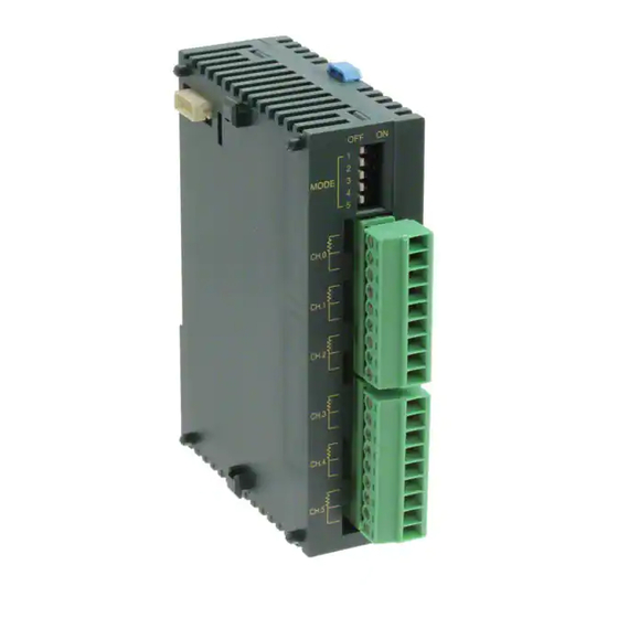
Chapter 2 Control Units Parts and Terminology ......2 − 3 2.1.1 Control Unit Types . - Page 26 Optional Memory Pin Layouts ........2 − 22 2.4.1 C10RS/C10CRS/C10RM/C10CRM .
- Page 27 Optional Memory Parts and Terminology Parts and Terminology There are sixteen different control unit types available: C10RS terminal type C14RS terminal type C10CRS (with RS232C port) terminal type C14CRS (with RS232C port) terminal type C10RM connector type C14RM connector type C10CRM (with RS232C port) connector type C14CRM (with RS232C port) connector type C16T...
-
Page 28: Control Unit Types
Optional Memory Parts and Terminology 2.1.1 Control Unit Types C10RS/C14RS C10RM/C14RM All control unit types C10CRS/C14CRS C10CRM/C14CRM (terminal type) (connector type) EXPANSION CONNECTOR C16T/C16CT C32T/C32CT Control unit with RS232C port C16P/C16CP C32P/C32CP T32CT/T32CP 2 − 4... -
Page 29: Mode Switch
51067−0900) (*section 7.7). Expansion hook 13 16 is used to secure expansion units. The hook is also used for installation on FP0 flat type mounting plate (AFP0804). Expansion connector connects an expansion unit to the internal circuit of the control unit (*section 6.1). -
Page 30: Tool Port
Mode Switch 2.1.1.2 This switch turns ON and OFF (RUN/PROG.) the operation of the FP0. The FP0 can also be turned ON and OFF by the programming tool. Switch position Operation mode RUN (upward) This sets the RUN mode. - Page 31 Optional Memory Specifications Specifications 2.2.1 General Specifications Item Description Rated operating voltage 24 V DC Operating voltage range 21.6 V to 26.4 V DC (*section 2.2.1.2 Rated current consumption 300 mA or less Allowed momen- C10/C14 5 ms at 21.6 V, 10 ms at 24 V tary power off time ff ti C16/C32...
-
Page 32: Current Consumed By The Control Unit
) FP0 Control unit FP0−C10 100mA or less — 25.8mA or less — FP0−C14 100mA or less — 34.4mA or less — FP0−C16 40mA or less —... - Page 33 Optional Memory Specifications Current consumption example C14RS E32T E16T E16RS At power supply connector of expansion I/O unit FP0 E16RS Type Current consumption FP0 E16RS 100 mA At power supply connector of control unit Type Current consumption FP0 C14RS 100 mA...
-
Page 34: Performance Specifications
Optional Memory Specifications 2.2.2 Performance Specifications Item Relay output type Transistor output type S−LINK type C10RS/ C14RS/ C16T/ C32T/ T32C C10RM/ C14RM/ C16P/ C32P/ C10CRS/ C14CRS/ C16CT/ C32CT/ C10CRM C14CRM C16CP C32CP Programming method/Control method Relay symbol/Cyclic operation Controllable I/O Total: 32 Basic unit Total: 10... - Page 35 Optional Memory Specifications Item Relay output type Transistor output type S−LINK type C10RS/ C14RS/ C16T/ C32T/ T32C C10RM/ C14RM/ C16P/ C32P/ C10CRS/ C14CRS/ C16CT/ C32CT/ C10CRM C14CRM C16CP C32CP Number of step ladders 128 stages 704 stages 128 stages (* Note 1) Number of subroutines 16 subroutines 100 sub-...
- Page 36 Optional Memory Specifications Relay output type Transistor output type S−LINK Item type C10RS/ C14RS/ C16T/ C32T/ T32C C10RM/ C14RM/ C16P/ C32P/ C10CRS/ C14CRS/ C16CT/ C32CT/ C10CRM C14CRM C16CP C32CP Special Pulse Output point Not available Two independent points (Y0 and functions u c o s output...
- Page 37 (F168) is executed. 11) Precautions when using the battery backup function Secondary (chargeable) battery is used as backup battery in the FP0 T32C control unit. The battery is not charged before the unit is shipped, so please make sure that the built−in backup battery have been charged before using the unit.
-
Page 38: Input Specifications
Optional Memory Specifications 2.2.3 Input Specifications Item Description Insulation method optical coupler Rated input voltage 24 V DC Rated input current approx. 4.3 mA (at 24 V DC) Input impedance approx. 5.6 kΩ Operating voltage range 21.6 to 26.4 V DC Input points per C10RM, 6 points/common... - Page 39 Limitations on Number of Simultaneous Input ON Points Keep the number of input points per common which are simultaneously ON within the following range as determined by the temperature. FP0-C14RM/C14CRM/C14RS/C14CRS at 24 V DC Number of at 26.4 V DC...
-
Page 40: Output Specifications
Optional Memory Specifications 2.2.4 Output Specifications 2.2.4.1 Relay Output Type FP0 relay output types: C10RM, C10CRM, C10RS, C10CRS, C14RM, C14CRM, C14RS, C14CRS Item Description Output type Normally open (1 Form A) relay output Rated control capacity 2 A 250 V AC, 2 A 30 V DC (4.5 A maximum per common) - Page 41 Optional Memory Specifications 2.2.4.2 Transistor Output Type FP0 transistor output types: C16T, C16CT, C16P, C16CP, C32T, C32CT, C32P, C32CP, T32CT, T32CP Item Description Insulation method optical coupler Output type open collector Rated load voltage NPN open collector type: 5 to 24 V DC (* Note)
- Page 42 Optional Memory Internal Circuit Diagram Internal Circuit Diagram 2.3.1 Relay Output Type (C10RS/C10CRS/C10RM/C10CRM/C14RS/C14CRS/C14RM/C14CRM) FP0-C10RS/C10CRS/C10RM/C10CRM/C14RS/C14CRS/C14RM/C14CRM Input side 5.6 kΩ Internal (* Note 1) circuit 5.6 kΩ Internal (* Note circuit 24 V DC (* Note 2) Output side Internal circuit Internal...
- Page 43 When the load voltage and external power supply are the same This example is when the values of the rated load voltage and external power supply for driving internal circuit are the same. In this situation, there is only one power supply. FP0-C16T/C16CT/C32T/C32CT Input side 5.6 kΩ...
- Page 44 When the load voltage differs from the 24 V DC external power supply for the driving the internal circuit Other than 24 V DC load voltage, 5 V DC and 12 V DC and other load voltages can be connected. FP0-C16T/C16CT/C32T/C32CT/T32CT Input side 5.6 kΩ Internal...
- Page 45 Optional Memory Internal Circuit Diagram 2.3.2.2 PNP Open Collector Type (C16P/C16CP/C32P/C32CP/T32CP) FP0-C16P/C16CP/C32P/C32CP/T32CP Input side 5.6 kΩ Internal (* Note 1) circuit 5.6 kΩ (* Note 1) 24 V DC Internal (* Note 2) circuit Output side (−) Internal Load circuit...
- Page 46 Optional Memory Pin Layouts Pin Layouts 2.4.1 C10RS/C10CRS/C10RM/C10CRM X0−5 C10RS/C10CRS C10RM/C10CRM Input X0−5 X0−5 (NC) (NC) (* Note) Y0−3 Y0−3 Output Load Load Y0−3 (NC) (NC) Power supply Load Load Power supply 2.4.2 C14RS/C14CRS/C14RM/C14CRM X0−7 C14RS/C14CRS C14RM/C14CRM Input X0−7 X0−7 (* Note) Y0−5 Output...
- Page 47 Optional Memory Pin Layouts 2.4.3 C16T/C16CT Input C16T/C16CT X0−7 (* Note 1) Output Y0−7 Load Load (−) Load Load Load Load Load Load (−) Notes The two COM terminals of input terminal (X0−7) are connected internally, however they should be externally connected as well.
- Page 48 Optional Memory Pin Layouts 2.4.4 C16P/C16CP Input C16P/C16CP X0−7 (* Note 1) Output Y0−7 Load Load (−) Load Load Load Load Load Load (−) Notes The two COM terminals of input terminal (X0−7) are connected internally, however they should be externally connected as well.
- Page 49 Optional Memory Pin Layouts 2.4.5 C32T/C32CT/T32CT Input Input C32T/C32CT X0 X1 (* Note 1) Output Output Y8 Y9 (−) (+) (−) Notes The four COM terminals of input terminals (X0−7 and X8−F) are connected internally, however they should be externally connected as well.
- Page 50 Optional Memory Pin Layouts 2.4.6 C32P/C32CP/T32CP Input Input C32P/C32CP X0 X1 (* Note 1) Output Output Y8 Y9 (−) (+) (−) (−) (−) Notes The four COM terminals of input terminals (X0−7 and X8−F) are connected internally, however they should be externally connected as well.
- Page 51 Optional Memory Backing Up the 10 K Step Type Backing Up the 10 K Step Type Recharging the internal backup battery A secondary battery (rechargeable type) is used as the backup battery in the control unit (10 K step type). When shipped, this battery is not charged; therefore, please make sure it is sufficiently charged before using.
- Page 52 Optional Memory Backing Up the 10 K Step Type Predicted life of internal backup battery When the control unit is on (when power is supplied) the internal backup battery life will differ depending on the ambient temperature. Refer to the table below to predict the life of the internal backup battery.
- Page 53 Chapter 3 Expansion I/O Units Parts and Terminology ......3 − 3 3.1.1 Expansion I/O Unit Types .
-
Page 54: E16Yt
Expansion I/O Units Pin Layouts ........3 − 18 3.4.1 E8RS/E8RM . - Page 55 Expansion I/O Units Parts and Terminology Parts and Terminology There are fourteen different expansion I/O unit types available: E8RS terminal type E16RS terminal type E8RM connector type E16RM connector type E16T E16P E32T E32P E8X input type E16X input type E8YT output type E8YP output type E16YT output type...
- Page 56 Expansion I/O Units Parts and Terminology 3.1.1 Expansion I/O Unit Types E8RS/E16RS E8RM/E16RM E16T/E16P E32T/E32P (terminal type) (connector type) E16YT/E16YP E8YT/E8YP E16X All expansion I/O unit types 3 − 4...
-
Page 57: Expansion Connector
I/O unit (*section 6.1). DIN rail attachment lever allows simple attachment to a DIN rail. The lever is also used for installation on FP0 slim type mounting plate (AFP0803). 3 − 5... -
Page 58: General Specifications
Expansion I/O Units Specifications Specifications 3.2.1 General Specifications For more details on the general specifications, refer to section 2.2.1. 3.2.2 Input Specifications Item Description Insulation method optical coupler Rated input voltage 24 V DC Rated input current approx. 4.3 mA (at 24 V DC) Input impedance approx. - Page 59 Limitations on Number of Simultaneous Input ON Points Keep the number of input points per common which are simultaneously ON within the following range as determined by the temperature. FP0-E16RS/E16RM at 24 V DC at 26.4 V DC Number of...
- Page 60 Expansion I/O Units Specifications 3.2.3 Output Specifications 3.2.3.1 Relay Output Type FP0 relay output types: E8RS, E8RM, E16RS, and E16RM Item Description Output type Normally open (1 Form A) relay output Rated control capacity 2 A 250 V AC, 2 A 30 V DC (4.5 A maximum per common)
- Page 61 Expansion I/O Units Specifications 3.2.3.2 Transistor Output Type FP0 transistor output types: E16T, E16P, E32T, E32P, E8YT, E8YP, E16YT, E16YP Item Description Insulation method optical coupler Output type open collector Rated load voltage NPN open collector type: 5 to 24 V DC (* Note)
- Page 62 Expansion I/O Units Internal Circuit Diagram Internal Circuit Diagram 3.3.1 Relay Output Type (E8RS/E8RM/E16RS/E16RM) FP0-E8RS/E8RM/E16RS/E16RM Input side 5.6 kΩ Internal 1 kΩ circuit 5.6 kΩ Internal 1 kΩ circuit 24 V DC (* Note) Output side Internal circuit Internal circuit...
- Page 63 When the load voltage and external power supply are the same This example is when the values of the rated load voltage and external power supply for driving internal circuit are the same. In this situation, there is only one power supply. FP0-E16T/E32T Input side 5.6 kΩ...
- Page 64 When the load voltage differs from the 24 V DC external power supply for the driving the internal circuit Other than 24 V DC load voltage, 5 V DC and 12 V DC and other load voltages can be connected. FP0-E16T/E32T 5.6 kΩ Internal 1 kΩ...
- Page 65 Expansion I/O Units Internal Circuit Diagram 3.3.2.2 PNP Open Collector Type (E16P/E32P) FP0-E16P/E32P Input side 5.6 kΩ Internal 1 kΩ circuit 5.6 kΩ 24 V DC Internal 1 kΩ (* Note) circuit Output side (−) Internal Load circuit Internal Load...
- Page 66 Expansion I/O Units Internal Circuit Diagram 3.3.3 Expansion Input Units (E8X/E16X) FP0-E8X/E16X Input side 5.6 kΩ Internal 1 kΩ circuit 5.6 kΩ Internal 1 kΩ circuit 24 V DC (* Note) Notes Either positive or negative polarity is possible for the input voltage supply.
- Page 67 When the load voltage and external power supply are the same This example is when the values of the rated load voltage and external power supply for driving the internal circuit are the same. In this situation, there is only one power supply. FP0-E8YT/E16YT Output side Internal Load...
- Page 68 When the load voltage differs from the 24 V DC external power supply for the driving the internal circuit Other than 24 V DC load voltage, 5 V DC and 12 V DC and other load voltages can be connected. FP0-E8YT/E16YT Output side Load (for 5 V ) Internal circuit...
- Page 69 Expansion I/O Units Internal Circuit Diagram 3.3.4.2 PNP Open Collector Type (E8YP/E16YP) FP0-E8YP/E16YP Output side (−) Internal Load circuit Internal Load circuit 24 V DC Note The output number given above is the output number when the expansion output unit is installed as the first expansion unit (*section 5.3).
- Page 70 Expansion I/O Units Pin Layouts Pin Layouts 3.4.1 E8RS/E8RM Input E8RS E8RM X0−3 X0−3 (NC) (NC) (NC) (NC) Y0−3 Y0−3 (* Note) Output Load Load Load Load (NC) (NC) (NC) (NC) Power supply Notes Either positive or negative polarity is possible for the input voltage supply.
- Page 71 Expansion I/O Units Pin Layouts 3.4.2 E16RS/E16RM Input E16RS E16RM (* Note) Output Load Load Load Load Load Load Load Load Power supply Notes Either positive or negative polarity is possible for the input voltage supply. The I/O number given above is the I/O number when the expansion I/O unit is installed as the first expansion unit.
- Page 72 Expansion I/O Units Pin Layouts 3.4.3 E16T Input E16T (* Note 1) Output Load Load (−) Load Load Load Load Load Load (−) Notes The two COM terminals of input terminals are connected internally, however they should be externally connected as well.
- Page 73 Expansion I/O Units Pin Layouts 3.4.4 E16P Input E16P (* Note 1) Output Load Load (−) Load Load Load Load Load Load (−) Notes The two COM terminals of input terminals are connected internally, however they should be externally connected as well.
- Page 74 Expansion I/O Units Pin Layouts 3.4.5 E32T Input Input E32T X20 X21 X20 X21 X28 X29 X22 X23 X2A X2B X24 X25 X2C X2D X26 X27 X2E X2F COM COM COM COM (* Note 1) Output Output Y28 Y29 Y20 Y21 Y28 Y29 Y22 Y23 Y2A Y2B...
- Page 75 Expansion I/O Units Pin Layouts 3.4.6 E32P Input Input E32P X20 X21 X20 X21 X28 X29 X22 X23 X2A X2B X24 X25 X2C X2D X26 X27 X2E X2F COM COM COM COM (* Note 1) Output Output Y28 Y29 Y20 Y21 Y28 Y29 Y22 Y23 Y2A Y2B...
- Page 76 Expansion I/O Units Pin Layouts 3.4.7 Input (* Note 1) Notes The two COM terminals of input terminals are connected internally, however they should be externally connected as well. 1) Either positive or negative polarity is possible for the input voltage supply.
- Page 77 Expansion I/O Units Pin Layouts 3.4.8 E16X E16X Input X28 X29 X20 X21 X28 X29 X22 X23 X2A X2B X24 X25 X2C X2D X26 X27 X2E X2F COM COM COM COM (* Note 1) Notes The four COM terminals of input terminals are connected internally, however they should be externally connected as well.
- Page 78 Expansion I/O Units Pin Layouts 3.4.9 E8YT E8YT Output Load Load Load Load Load Load Load Load (−) (−) 3.4.10 E8YP E8YP Output Load Load Load Load Load Load Load Load (−) (−) Note The output number given above is the output number when the expansion output unit is installed as the first expansion unit.
- Page 79 Expansion I/O Units Pin Layouts 3.4.11 E16YT E16YT Output Output Y20 Y21 Y28 Y29 Load Load Load Load Load Load Load Load Load Load Load Load Load Load Load Load (−) (−) (−) Notes The two (+) terminals of the output terminals are connected internally, however they should be externally connected as well.
-
Page 80: E16Yp
Expansion I/O Units Pin Layouts 3.4.12 E16YP E16YP Output Output Y28 Y29 Y20 Y21 Load Load Load Load Load Load Load Load Load Load Load Load Load (−) Load Load Load (−) (−) Notes The two (+) terminals of the output terminals are connected internally, however they should be externally connected as well. - Page 81 Chapter 4 S−LINK Control Unit Names and Functions ......4 − 3 Specifications .
- Page 82 S−LINK Control Unit 4 − 2...
-
Page 83: Chapter 4 S−Link Control Unit
S−LINK Control Unit Names and Functions Names and Functions Status indicator LED The LED display the operation mode and error statuses. ERROR ADDRESS display (2−digit hexadecimal display) The address at which the S−LINK system error occurred is displayed. Mode switch The mode switch changes the operation mode. - Page 84 The power supply and signal wires of the S−LINK system are connected to the S−LINK terminal block. The S−LINK terminal block can be detached from the FP0 S−LINK control unit for wiring operations. For detailed information, refer to section “4.3.2 Wiring to S−LINK Terminal Block.”...
-
Page 85: Specifications
S−LINK Control Unit Specifications Specifications 4.2.1 General Specifications Item Description Rated operating voltage 24V DC Operating voltage range 21.6V to 26.4V DC Rated current consumption 150mA or less Allowed momentary power off time 10ms at 21.6V, 10ms at 24V Ambient temperature 0°C to +55°C/32°F to +131°F Storage temperature −20°C to +70°C/−4°F to +158°F... -
Page 86: S−Link Controller Specifications
FAN−out total > or = the FAN−in total. (For detailed information on calculating the FAN−in value and other values, see the “S−LINK Design Manual.” 3) The FP0 S−LINK control unit does not have a loop wiring function. 4 − 6... -
Page 87: Wiring The Power Supply
S−LINK Control Unit Wiring the Power Supply Wiring the Power Supply With the FP0 S−LINK control unit, power must be supplied at two locations (power supply connector and S−LINK terminal block). 4.3.1 Wiring to Power Supply Connector This is the power supply for the programmable controller section and the S−LINK controller in the S−LINK control unit (24V DC, 150mA). - Page 88 S−LINK Control Unit Wiring the Power Supply S−LINK terminal block: MC1.5/6−ST−3.5 (Made by Phoenix Contact Co.) Terminal name Color of connecting cable Description Brown Main wire (for S−LINK I/O devices) Blue White Black IN−24V — External power supply input for S−LINK IN−0V —...
-
Page 89: Sequence Of Turning On Power Supplies
S−LINK Control Unit Sequence of Turning on Power Supplies Sequence of Turning on Power Supplies When turning on the power supplies to the S−LINK control unit, follow the sequence outlined below. Procedure: Turn on the power supply to the S−LINK I/O devices connected to the S−LINK system. -
Page 90: Operation When Power Supply Is Turned On
Operation When Power Supply is Turned On Refreshing S−LINK I/O data With the S−LINK control unit, I/O data is refreshed by the CPUs of both the FP0 section and the S−LINK section, through the memory shared between them. S−LINK control unit... -
Page 91: S−Link System Address Recognition
S−LINK Control Unit S−LINK System Address Recognition S−LINK System Address Recognition 4.6.1 Recognizing the Address Before the S−LINK system is being operated for the first time, turn on the power supply and then press the system SET button. When the system SET button is pressed, the number of connected devices recognized by S−LINK control unit blinks on the error address display in hexadecimal. -
Page 92: Address Setting Of S−Link I/O Device
Up to seven boosters can be connected to one system for any individual S−LINK control unit, but the actual number which can be connected varies depending on the units configuring the system and the wiring length. Note The FP0 S−LINK control unit does not have a loop wiring function. 4 − 12... -
Page 93: Judging Errors From The Error Indicators
S−LINK. 2) ERR4 is held, so to cancel it, one of the following is required: turn the power supply to the FP0 off and then on again, press the system SET button and enter the settings again, or turn the power supply on the S−LINK side off and then on again. -
Page 94: Judging Errors Address Displays
S−LINK Control Unit Judging Errors Address Displays Judging Errors Address Displays The transmission line is monitored at all times, and if an error occurs, the address at which the error occurred is displayed as a hexadecimal value. ERROR indicator ERROR ADDRESS display During normal transmission:... -
Page 95: Chapter 5 I/O Allocation
Chapter 5 I/O Allocation I/O Number ........5 −... - Page 96 I/O Allocation 5 − 2...
-
Page 97: I/O Number
..Specifying X and Y numbers On the FP0, the same numbers are used for input and output. Example: The same number “X20 and Y20” can be used for input and output 5 − 3... -
Page 98: Control Unit
I/O Allocation Control Unit Control Unit The I/O allocation of the FP0 control unit is fixed. Type I/O number C10RS, C10CRS, C10RM, C10CRM Input: 6 points X0 to X5 Output: 4 points Y0 to Y3 C14RS, C14CRS, C14RM, C14CRM Input: 8 points... -
Page 99: Expansion I/O Unit
Y40 to Y5F Y60 to Y7F − The channel data of FP0−A80, TC4, TC8, A04V and A04I will switch and be read or written by a user program that contains the conversion data switch flag. − Please verify with the manual for the FP0 CC−Link Slave unit. - Page 100 I/O Allocation Expansion I/O Unit 5 − 6...
-
Page 101: Chapter 6 Installation
......6 − 8 Installation Using FP0 Slim Type Mounting Plate .. - Page 102 Installation 6 − 2...
-
Page 103: Adding Expansion Units
Installation Adding Expansion Units Adding Expansion Units Expansion method Peel the seal on the side of the unit so that the internal connector is exposed. Seal Notes When peeling the seal on the side of the initial lot products, the shaded part is exposed. Cut off the shaded part with a pair of nippers or similar tool so that the internal connector is exposed. - Page 104 Installation Adding Expansion Units Raise the expansion hooks on the top and bottom sides of the unit with a screwdriver. Expansion hook Align the pins and holes in the four corners of the control unit and expansion unit, and insert the pins into the holes so that there is no gap between the units.
-
Page 105: Important Notes
Installation Important Notes Important Notes Please, read the following notes carefully before the installation of your FP0. Notes Avoid installing the unit in the following locations: − Ambient temperatures outside the range of 0°C to 55°C/32°F to 131°F − Ambient humidity outside the range of 30% to 85% RH −... - Page 106 − Always install the unit orientated with the tool port facing outward on the bottom in order to prevent the generation of heat. Tool port − Do not install the FP0 control unit as shown below. Upside-down I/O connectors or I/O terminals on top Installations such that the I/O...
- Page 107 50 mm/1.97 in. or more − Maintain a minimum of 100 mm/3.937 in. between devices to avoid adverse affects from noise and heat when installing a device or panel door to the front of the FP0 unit. 100mm/3.937 in. or more Other device or panel door −...
-
Page 108: Attachment To Din Rails
Attachment to DIN Rails The FP0 unit enables one-touch attachment to DIN rails. Procedure: Fit the upper hook of the FP0 unit onto the DIN rail. Without moving the upper hook, press on the lower hook to fit the FP0 unit into position. -
Page 109: Installation Using Fp0 Slim Type Mounting Plate
FP0 slim type mounting plate FP0 unit When using an expansion unit, tighten the screws after joining all of the FP0 slim type mounting plate to be connected. Tighten the screws at each of the four corners. Example: Two expansion units FP0 slim type mounting plate Dia. -
Page 110: Installation Using Fp0 Flat Type Mounting Plate
Use M4 size pan−head screws for attachment of FP0 flat type mounting plate (AFP0804) and install according to the dimensions shown below. For a diagram showing detailed dimensions of the FP0 flat type mounting plate, see *section 13.5. FP0 flat type... - Page 111 Installation 6.5 Installation Using FP0 Flat Type Mounting Plate An FP0 unit with an attached FP0 flat type mounting plate can also be installed sideways on a DIN rail. DIN rail FP0 flat type mounting plate 6 − 11...
- Page 112 Installation Installation Using FP0 Flat Type Mounting Plate 6 − 12...
-
Page 113: Chapter 7 Wiring
Chapter 7 Wiring Safety Instructions ......7 − 3 7.1.1 Interlock Circuit . - Page 114 Wiring 7 − 2...
-
Page 115: Safety Instructions
7.1.3 Start Up Sequence The FP0 should be operated after all of the outside devices are energized. To keep this sequence, the following measures are recommended: Set the mode switch from PROG. mode to RUN mode after power is... -
Page 116: Momentary Power Failures
7.1.4 Momentary Power Failures If the duration of the power failure is less than 5 ms, the FP0 continues to operate. If the power is OFF for 5 ms or longer, operation changes depending on the combination of units, the power supply voltage, and other factors. (In some cases, operation may be the same as that for a power supply reset.) -
Page 117: Wiring The Power Supply To The Control Unit
The regulator on the FP0 unit is a non-insulated type. If using a power supply device without an internal protective circuit, always make sure power is supplied to the unit through a protective element such as a fuse. - Page 118 If the input/output power supplies are turned OFF before the power to the control unit, the FP0 control unit may detect a drop in the input level, and malfunction. Be sure to supply power to a control unit and an expansion unit from the same power supply, and turn the power ON and OFF simultaneously for both.
-
Page 119: Grounding
CORRECT Notes The point of grounding should be as close to the FP0 control unit as possible. The ground wire should be as short as possible. If two devices share a single ground point, it may produce an adverse effect. - Page 120 Grounding When the plus side is grounded, do not ground the functional earth terminal. Do not ground the FP0 functional earth terminal if the plus terminal of the power supply is grounded. Depending on the PC, some types have the SG terminal of the RS232C port connected to the outside structure of the connector.
-
Page 121: Input Wiring
Wiring Input Wiring Input Wiring Notes Be sure to select the thickness (dia.) of the input wires while taking into consideration the required current capacity. Arrange the wiring so that the input and output wiring are separated, and so that the input wiring is separated from the power wiring, as much as possible. -
Page 122: Led-Equipped Reed Switch
R: Bleeder resistor (k Ω The OFF voltage of the FP0 input is 2.4 V, therefore, select an R value so that the voltage between the COM terminal and the input terminal will be less than 2.4 V. (The impedance of the FP0 input terminal is 5.6 kΩ.) 13.44... -
Page 123: Led-Equipped Limit Switch
Ω R: Bleeder resistor (k Ω The OFF voltage of the FP0 input is 2.4 V, therefore when the power supply voltage is 24 V, select R so that 24 - 2.4 the current will be greater than I = 13.44... -
Page 124: Output Wiring
Protective Circuit for Inductive Loads With an inductive load, a protective circuit should be installed in parallel with the load. When switching DC inductive loads with FP0 relay output type, be sure to connect a diode across the ends of the load. -
Page 125: Precautions For Using Capacitive Loads
Wiring Output Wiring When using a DC inductive load Diode (*) Output terminal DC inductive load (*) Diode: Reverse voltage (V ): 3 times the load voltage Average rectified forward current (I ): Load current or more 7.5.2 Precautions for Using Capacitive Loads When connecting loads with large in-rush currents, to minimize their effect, connect a protection circuit as shown below. -
Page 126: Wiring The Terminal Type
Wiring the Terminal Type Wiring the Terminal Type A screw-down connection type terminal block socket for terminal of FP0 control unit and analog I/O unit is used. The terminal block socket and suitable wires are given below. Terminal block socket... - Page 127 Wiring Wiring the Terminal Type Procedure: Remove a portion of the wire’s insulation. Suitable wire 7 mm/0.276 in. Insert the wire into the terminal block socket until it contacts the back of the block socket, and then tighten the screw clockwise to fix the wire in place. Clockwise Wire Notes...
-
Page 128: Wiring The Molex Connector Type
Wiring Wiring the MOLEX Connector Type Wiring the MOLEX Connector Type The housings and contacts listed below come supplied with the FP0. Use the wires given below. Also, use the required special tool for connecting the wires. Housing Contact Suitable wire... - Page 129 Wiring Wiring the MOLEX Connector Type Place the contact in the crimping tool, place the wire in the contact and lightly squeeze the tool. Crimping tool Wire Contact Insert the crimped wire into the housing until it contacts the back side. Housing Note When removing a wire, use a flat-head screwdriver, or other...
-
Page 130: Wiring The Mil Connector Type
Wiring the MIL Connector Type Wiring the MIL Connector Type The housings, semi-cover and pressure welders listed below come supplied with the FP0. Use the wires given below. Also, use the required pressure connection tools for connecting the wires. Supplied connector... -
Page 131: Contact Puller Pin For Rewiring
Wiring Wiring the MIL Connector Type After press-fitting the wire, insert it into the housing. When all wires has been inserted, fit the semi-cover into place. semi-cover Note If using a MIL connector for flat cables, please specify the order number AXM110915. -
Page 132: Wiring The Rs232C Port
Wiring Wiring the RS232C Port Wiring the RS232C Port When using the RS232C port, use the screw-down connection type terminal and the wire according to the following procedures. FP0 Control unit with RS232C port (FP0 C10CRM/C10CRS/C14CRM/C14CRS/C16CT/C16CP/C32CT/C32CP) Item Specification Baud rate... - Page 133 Wiring Wiring the RS232C Port When tightening the RS232C port, use a screwdriver (Phoenix Contact Co., Product no. 1205037) with a blade size of 0.4 × 2.5. The tightening torque should be 0.22 to 0.25 N⋅m (2.3 to 2.5 kgf⋅cm) or less. Procedure: Remove a portion of the wire’s insulation.
- Page 134 Wiring Wiring the RS232C Port Notes When removing the wire’s insulation, be careful not to scratch the core wire. Do not twist the wires to connect them. Do not solder the wires to connect them. The solder may break due to vibration. After wiring, make sure stress is not applied to the wire.
-
Page 135: Precautions During Programming
Chapter 8 Precautions During Programming Use of Duplicated Output ......8 − 3 8.1.1 Duplicated Output . - Page 136 Precautions During Programming 8.5.3 Precautions When Using a Control Instruction ......8 − 16 Precautions for Programming .
-
Page 137: Use Of Duplicated Output
Precautions During Programming Use of Duplicated Output Use of Duplicated Output 8.1.1 Duplicated Output Duplicated output refers to repeatedly specifying the same output in a program. If the same output is specified for the “OT” and “KP” instructions, it is considered to be duplicated output. -
Page 138: When Output Is Repeated
Precautions During Programming Use of Duplicated Output 8.1.2 When Output is Repeated with an OT, KP, SET, or RST Instruction Condition of Internal and Output Relays During Operation When instructions are repeatedly used which output to internal and output relays such as transfer instructions and OT, KP, SET and RST instructions, the contents are rewritten at each step during operation. -
Page 139: Handling Bcd Data
Precautions During Programming Handling BCD Data Handling BCD Data 8.2.1 BCD Data BCD is an acronym for binary−coded decimal, and means that each digit of a decimal number is expressed as a binary number. Example: Expressing a decimal number in BCD: Decimal number Each digit is converted to a binary number. - Page 140 Precautions During Programming Handling BCD Data Output to a 7−segment Display (with Decoder) Use the BIN−to−BCD conversion instruction “F80 (BCD)”. Data processed in (Conversion 0 0 0 0 0 1 1 1 1 1 0 0 1 0 0 0 PLC (BIN data) using ↓...
-
Page 141: Handling Index Registers
Precautions During Programming 8.3 Handling Index Registers Handling Index Registers 8.3.1 Index Registers Like other registers, index registers have two points, IX and IY, for reading and writing 16-bit data. Use an index register to indirectly specify a memory area number. (This is also called index modification.) Example: Transferring the contents of data register DT100 to the number... -
Page 142: Example Of Using An Index Register
Precautions During Programming Handling Index Registers 8.3.3 Example of Using an Index Register Repeatedly Reading in External Data Example: Writing the contents of word external input relay WX3 to a sequence of data registers beginning from DT0. F0 MV, K0, IX F0 MV, WX3, IXDT0 F35 +1, IX When R0 turns on, K0 is written to index register IX. - Page 143 Precautions During Programming 8.3 Handling Index Registers F81 BIN, WX1, IX F81 BIN, WX0, IXSV0 Convert the BCD timer number data in WX1 to binary and set it in index register IX. Convert the BCD timer set value in WX0 to binary and stored in the timer set value area SV specified by contents of IX.
-
Page 144: Operation Errors
An operation error is a condition in which operation is impossible when a high-level instruction is executed. When an operation error occurs, the ERROR/ALARM LED on the FP0 control unit will blink and the operation error flags (R9007 and R9008) will turn on. -
Page 145: Dealing With Operation Errors
Precautions During Programming Operation Errors 8.4.3 Dealing with Operation Errors Procedure: Check the location of the error. Check the address where the error occurred, which is stored in DT9017 and DT9018, and make sure the high−level instruction for that address is correct and appropriate. Clear the error. -
Page 146: Points To Check In Program
DT0. If data in IX is larger than the last address of the data register, an operation error will occur. If the PLC you are using is of the FP0 16-point type, the last address of the data register is DT1659. If the data in IX exceeds the range of K0 to K255, an operation error will occur. -
Page 147: Instruction Of Leading Edge Detection Method
Precautions During Programming 8.5 Instruction of Leading Edge Detection Method Instruction of Leading Edge Detection Method 8.5.1 Instructions of Leading Edge Detection Method Instructions Using the Leading Edge Detection Operation DF (leading edge differential) instructions Count input for CT instructions Count input for F118 (UDC) instructions Shift input for SR instructions Shift input for F119 (LRSR) instructions... -
Page 148: Operation And Precautions At Run Start Time
Precautions During Programming Instruction of Leading Edge Detection Method Precautions When Using an Instruction Which Performs Leading Edge Detection When RUN begins, for example when the system is powered on, the off → on change of the execution condition (trigger) is not detected. The instruction is not executed. Execution of the instruction will take place as explained on section 8.5.2. - Page 149 Precautions During Programming 8.5 Instruction of Leading Edge Detection Method Example 1: DF (leading edge differential) instruction Add R9014 R9014 (Power on) Even if X0 was initially on, the input condition (X0) for the DF instruction is off−to−on at the second scan, therefore derivative output is obtained.
-
Page 150: Precautions When Using A Control Instruction
Precautions During Programming Instruction of Leading Edge Detection Method 8.5.3 Precautions When Using a Control Instruction Instructions which leading edge detection compare the condition of the previous execution and the condition of the current execution, and execute the instruction only if the previous condition was off and the current condition is on. - Page 151 Precautions During Programming 8.5 Instruction of Leading Edge Detection Method Example 2: Using the CT instruction between JP and LBL instructions LBL 1 Time chart 1 Counting operation Final timing at The count is not incremented, because the final which the timing at which the previous JP instruction was not previous JP executed has not been changed, and the execution...
-
Page 152: Precautions For Programming
Precautions During Programming Precautions for Programming Precautions for Programming Programs which do not execute correctly Do not write the following programs as they will not execute correctly. Program example 1: Program in which the example 1 is rewritten Program example 2: Program in which the example 2 is rewritten TMX5, TMX 5, K 30... -
Page 153: Rewrite Function During Run
Operation of Rewrite During RUN How Operation of Rewrite During RUN The FP0 allows program rewriting even in RUN mode. When a rewrite is attempted during RUN, the tool service time is temporarily extended, program rewriting is performed, and operation is resumed without the need to change the mode. For this reason, the time of the scan during the RUN rewrite extends from several msec to several hundreds of msec. -
Page 154: Cases Where Rewriting During Run Is Not Possible
Precautions During Programming Rewrite Function During RUN 8.7.2 Cases Where Rewriting During Run is not Possible When the timeout error message is indicated: Even if the timeout error message is indicated, it is highly possible that the program in PLC has been already rewritten. Carry out the following operations. 1. - Page 155 Precautions During Programming 8.7 Rewrite Function During RUN Instructions which do not allow rewriting during RUN Step ladder instructions (SSTP/STPE) Subroutine instructions (SUB/RET) Interrupt instructions (INT/IRET) Control instructions (ED/LBL) (LBL instructions allow insertion and writing, but not deletion and clearing.) Instructions which do not allow rewriting to subprograms The following instructions do not allow rewriting during subroutines or interrupt programs.
-
Page 156: Procedures And Operation Of Rewrite During Run
Precautions During Programming Rewrite Function During RUN 8.7.3 Procedures and Operation of Rewrite During RUN Item FPWIN GR FPWIN GR FP Programmer II Ladder symbol mode Boolean mode Rewrite procedure Maximum of 128 steps. Rewriting performed by step. Changes are performed by Caution is required as rewriting takes place simulta- block. -
Page 157: Changing Program Modes
Precautions During Programming 8.7 Rewrite Function During RUN Item FPWIN GR FPWIN GR FP Programmer II Ladder symbol mode Boolean mode Operation of SSTP/STPE A distance with the same Writing and deletion of a single instruction is not each instruc- number cannot be defined possible for a program with no step ladder area. -
Page 158: Changing The Set Value Of Timer/Counter During Run
Precautions During Programming Changing the Set Value of Timer/Counter During RUN Changing the Set Value of Timer/Counter During RUN 8.8.1 Method of Rewriting Constant in FP Programmer II This method rewrites the Timer set value value in the program. TMX 5,K Rewrite Method Using FP Programmer II Example of changing the set value of timer 5 from K30 to K50 Procedure:... -
Page 159: Method Of Rewriting A Value In The Set Value Area
Precautions During Programming Changing the Set Value of Timer/Counter During RUN 8.8.2 Method of Rewriting a Value in the Set Value Area Transfers to SV area when mode changes to RUN mode. Timer set value TMX5, K This method rewrites the value in the set value area. - Page 160 Precautions During Programming Changing the Set Value of Timer/Counter During RUN Method 1: Method using the programming tool software Procedure: Select “Monitoring Registers” from the Online menu. Explanation of each column (1) Displays the line number. (2) Displays the device code and device number. (3) Displays the monitored data.
- Page 161 Precautions During Programming Changing the Set Value of Timer/Counter During RUN Method 2: Method using the FP Programmer II Use the word data monitor function to read the set value area SV of the timer or counter to be changed, and rewrite the value. Example of changing the value of SV0 from K30 to K50.
-
Page 162: Processing During Forced Input And Output
Precautions During Programming Processing During Forced Input and Output Processing During Forced Input and Output Processing when forced input/output is initiated during RUN Forced reset / reset processing Input/output update Forced set / reset processing Operation Forced set / reset processing Peripheral service Processing of external input (X) Regardless of the state of the input from the input device, forced on/off operation will... -
Page 163: Setting The Clock/Calendar Timer (T32Ct Type Only)
Precautions During Programming 8.10 Setting the Clock/Calendar Timer (T32CT type only) 8.10 Setting the Clock/Calendar Timer (T32CT type only) Ckock/Calendar timer setting area The write area and read area for clock/calendar timer is allocated to special data registers DT90053 to DT90057. Special data register Upper byte Lower byte... - Page 164 Precautions During Programming 8.10 Setting the Clock/Calendar Timer (T32CT type only) − Setting and changing using a program 1. Transfer the value to be written into special data registers DT90054 to DT90057 that are allocated in clock/calendar timer setting area. 2.
- Page 165 Chapter 9 High−speed Counter/Pulse Output/ PWM Output Outline of Functions ......9 − 3 9.1.1 Three Functions that Use Built−in High−speed Counter...
- Page 166 High−speed Counter/Pulse Output/ PWM Output PWM Output Function ......9 − 33 9.5.1 Outline of PWM Output Function .
-
Page 167: Outline Of Functions
Three Functions that Use Built−in High−speed Counter Functions that use the built−in high−speed counter There are three functions available when using the high−speed counter built into the FP0. High−speed counter function The high−speed counter function counts external inputs such as those from sensors or encoders. -
Page 168: Performance Of Built−In High−Speed Counter
High−speed Counter/Pulse Output/ PWM Output Outline of Functions PWM output function By using the appropriate instruction, the PWM output function enables a pulse output of the desired duty ratio. When you increase the pulse width... heating increases. When you decrease it... heating decreases. -
Page 169: Specifications And Restricted Items
High−speed Counter/Pulse Output/ PWM Output 9.2 Specifications and Restricted Items Specifications and Restricted Items 9.2.1 Specifications Table of high−speed counter function specifications Input/output contact number Built−in Memory area used Performance specifica- Related being used high− tions instruc- speed speed tions tions On/off Count... - Page 170 High−speed Counter/Pulse Output/ PWM Output Specifications and Restricted Items Table of pulse output function specifications Input/output contact number being used Built−in Memory area used Performance Related high− high specifications specifications instruc- instruc speed for maximum tions Pulse Direc- Home Near Con- Elapsed Target...
-
Page 171: Functions And Restrictions
High−speed Counter/Pulse Output/ PWM Output 9.2 Specifications and Restricted Items 9.2.2 Functions and Restrictions Channel The same channel cannot be used by more than one function. Example of prohibited application: You cannot share CH0 with the high−speed counter and pulse output functions. I/O number (input/output contact point) The number allocated to each function cannot be used for normal input or outputs. - Page 172 High−speed Counter/Pulse Output/ PWM Output Specifications and Restricted Items Restrictions for maximum counting speed/pulse output frequency The counting speed when using the high−speed counter function will differ depending on the counting mode as shown in the table. Example 1: While in the incremental input mode and using the two channels CH0 and CH1, if CH0 is being used at 8 kHz, then CH1 can be used up to 2 kHz.
-
Page 173: Outline Of High−Speed Counter Function
High−speed Counter/Pulse Output/ PWM Output 9.3 High−speed Counter Function High−speed Counter Function 9.3.1 Outline of High−speed Counter Function High−speed counter function The high−speed counter function counts the input signals, and when the count reaches the target value, turns on and off the desired output. The high−speed counter function is able to count high−speed pulses of frequencies up to 10 kHz. - Page 174 High−speed Counter/Pulse Output/ PWM Output High−speed Counter Function 2−phase input mode (Incremental input: CW) Count n−1 (Decremental input: CCW) Count n−1 n−2 n−3 Incremental/decremental input mode (separate input mode) Count Increasing Decreasing Increasing Decreasing Directional distinction mode Count Increasing Decreasing 9 −...
- Page 175 High−speed Counter/Pulse Output/ PWM Output 9.3 High−speed Counter Function 9.3.3 I/O Allocation The inputting, as shown in the table on section 9.2.1, will differ depending on the channel number being used. The output turned on and off can be specified from Y0 to Y7 as desired with instructions F166 and F167.
-
Page 176: Instructions Used With High−Speed Counter Function
High−speed Counter/Pulse Output/ PWM Output High−speed Counter Function 9.3.4 Instructions Used with High−speed Counter Function High−speed counter control instruction (F0) This instruction is used for counter operations such as software reset and count disable. Specify this instruction together with the F0 (MV) instruction and the special data register DT9052/DT90052. - Page 177 High−speed Counter/Pulse Output/ PWM Output 9.3 High−speed Counter Function Example 2: Reads the elapsed value of the high−speed counter and copies it to DT100. F1 DMV, DT9044, DT100 Each time the ED instruction is executed, the elapsed value is automatically transferred from the elapsed value area to the special data registers DT9044 and DT9045/ DT90044 and DT90045.
-
Page 178: Sample Program
High−speed Counter/Pulse Output/ PWM Output High−speed Counter Function 9.3.5 Sample Program Wiring examples Input terminal Operation start Encoder input Encoder Motor Output terminal Inverter Operation Operation/Stop − Speed 5,000 Number of pulse 9 − 14... - Page 179 High−speed Counter/Pulse Output/ PWM Output 9.3 High−speed Counter Function Positioning operations with a single speed inverter When X5 is turned on, Y0 turns on and the conveyor begins moving. When the elapsed value (DT9044 and DT9045) reaches K5000, Y0 turns off and the conveyor stops. R903A R102 R100...
- Page 180 High−speed Counter/Pulse Output/ PWM Output High−speed Counter Function Wiring example Input terminal Encoder input Operation start Encoder Motor Output terminal Inverter Run/Stop High−speed Fast/Slow switching − Speed 4,500 5,000 Number of pulse 9 − 16...
- Page 181 High−speed Counter/Pulse Output/ PWM Output 9.3 High−speed Counter Function Positioning operations with a double speed inverter When X5 is turned on, Y0 and Y1 turn on and the conveyor begins moving. When the elapsed value (DT9044 and DT9045) reaches K4500, Y1 turns off and the conveyor begins decelerating.
-
Page 182: Outline Of Pulse Output Function
High−speed Counter/Pulse Output/ PWM Output Pulse Output Function Pulse Output Function 9.4.1 Outline of Pulse Output Function Instructions used and control settings The pulse function enables positioning control by use in combination with a commercially available pulse−string input type motor driver. Provides trapezoidal control with the instruction F168 for automatically obtaining pulse outputs by specifying the initial speed, maximum speed, acceleration/deceleration time, and target value. -
Page 183: Control Mode
High−speed Counter/Pulse Output/ PWM Output Pulse Output Function 9.4.2 Control Mode Incremental <relative value control> Outputs the pulse of the pulse number set by the target value. By setting H02 (incremental; forward: off; reverse: on) in the control code with instruction F168, when the target value is positive, the directional output is turned off and the elapsed value of the high−speed counter increases. -
Page 184: I/O Allocation And Wiring
High−speed Counter/Pulse Output/ PWM Output Pulse Output Function 9.4.3 I/O Allocation and Wiring Single pulse input driver (pulse input and directional switching input) One output point is used as a pulse output and the other output is used as a directional output. - Page 185 Caution when using a double pulse input driver When using the FP0 pulse outputs Y0 and Y1 for direct connection to the CW input and CCW input of a driver, the counter elapsed values for the separate channels (ch0 and ch1) increase and decrease in response to the individual outputs.
-
Page 186: Instructions Used With Pulse Output Function
High−speed Counter/Pulse Output/ PWM Output Pulse Output Function 9.4.4 Instructions Used with Pulse Output Function Positioning control instruction (F168) Automatically performs trapezoidal control according to the specified data table. F0 MV, H102, DT100 F0 MV, K500, DT101 F0 MV, K5000, DT102 F0 MV, K200, DT103 F1 DMV, K10000, DT104 F0 MV, K0, DT106... - Page 187 High−speed Counter/Pulse Output/ PWM Output Pulse Output Function Pulse output instruction (F169) This instruction is for JOG operation by obtaining a pulse from the desired output when the execution condition (trigger) turns on. F0 MV, H112, DT200 F0 MV, K300, DT201 F169 PLS, DT200, H0 While X2 is in the on state, a pulse of 300 Hz with a duty ratio of 10% is output from Y0.
- Page 188 High−speed Counter/Pulse Output/ PWM Output Pulse Output Function Example 1: Enable the near home input during home return operations and begin deceleration..F0 MV, H 4 , DT9052 ..F0 MV, H 0 , DT9052 In the above program, the near home input is enabled in step and 0 is entered just after that in step to perform the preset operations.
-
Page 189: Sample Program For Positioning Control
High−speed Counter/Pulse Output/ PWM Output Pulse Output Function 9.4.5 Sample Program for Positioning Control Wiring example Input terminal Home sensor Positioning start Positioning start Home return start Near home sensor Forward JOG start Reverse JOG start Overrun a contact b contact a contact b contact Moving table Stepping motor... - Page 190 High−speed Counter/Pulse Output/ PWM Output Pulse Output Function Relative value positioning operation (plus direction) When X1 turns on, a pulse is output from Y0. At this time, directional output Y2 does not turn on. R903A Positioning operations running Positioning operations start DT100 Control code: H102 F0 MV, H 102, DT 100 [refer to “instruction...
- Page 191 High−speed Counter/Pulse Output/ PWM Output Pulse Output Function Relative value positioning operation (minus direction) When X2 turns on, a pulse is output from Y0. At this time, directional output Y2 turns R903A Positioning operations running Positioning operations start DT100 Control code: H102 F0 MV, H 102, DT 100 [refer to “instruction F168 (SPD1)”]...
- Page 192 High−speed Counter/Pulse Output/ PWM Output Pulse Output Function Absolute value positioning operation When X1 is turned on, pulses are output from Y0. If the current value at that point is larger than ”22,000”, the direction output Y2 goes on, and if the value is smaller than ”22,000”, the direction output Y2 does not go on.
- Page 193 High−speed Counter/Pulse Output/ PWM Output Pulse Output Function Home return operation (minus direction) When X3 turns on, a pulse is output from Y0 and the return to home begins. At this time, directional output Y2 turns on. Then, when X4 turns on, deceleration begins, and when X0 turns on, home return is completed.
- Page 194 High−speed Counter/Pulse Output/ PWM Output Pulse Output Function Home return operation (plus direction) When X3 turns on, a pulse is output from Y0 and the return to home begins. At this time, directional output Y2 does not turn on. Then, when X4 turns on, deceleration begins, and when X0 turns on, home return is completed.
- Page 195 High−speed Counter/Pulse Output/ PWM Output Pulse Output Function JOG operation (plus direction) While X5 is in the on state, a pulse is output from Y0. At this time, directional output Y2 does not turn on. F0 MV, H 112, DT 300 DT300 Control code: H112 [refer to “instruction F0 MV, K 300, DT 301...
- Page 196 High−speed Counter/Pulse Output/ PWM Output Pulse Output Function Troubleshooting flowchart if a pulse is not output when instruction F168 (SPD1) executed Error occurs [F168 SPD1, ϕ , Kϕ ] Remedy Special internal Remedy problem relay R903A or R903B Not set to K0 or K1. problem is already on.
-
Page 197: Pwm Output Function
High−speed Counter/Pulse Output/ PWM Output PWM Output Function PWM Output Function 9.5.1 Outline of PWM Output Function PWM output function With the instruction F170 (PWM), the specified duty ratio and pulse width modulation is obtained. Applicable to analog controls such as temperature control and light modulation. Setting the system register When using the PWM output function, set the channels corresponding to system registers 400 to “Do not use high−speed counter.”... - Page 198 High−speed Counter/Pulse Output/ PWM Output PWM Output Function 9 − 34...
-
Page 199: Data Reception
Chapter 10 General−use Serial Communications 10.1 General−use Serial Communications Function ..10 − 3 10.1.1 General−use Serial Communications ..10 − 3 10.1.2 Data Transmission ..... 10 −... - Page 200 General−use Serial Communications 10 − 2...
-
Page 201: Data Transmission
General−use Serial Communications 10.1 General−use Serial Communications Function 10.1 General−use Serial Communications Function 10.1.1 General−use Serial Communications Using the RS232C port, data and commands can be sent to and received from an external device such as a bar code reader. This is done by executing the F144 (TRNS) instruction. - Page 202 General−use Serial Communications 10.1 General−use Serial Communications Function 10.1.3 Data Reception Data sent from an external device is received at the RS232C port. The received data is automatically stored in the data register specified as the reception buffer. (For details see “F144 (TRNS)” instruction.) Data registers used as reception buffers are specified by system register 417 and 418.
- Page 203 General−use Serial Communications 10.2 System Register Settings 10.2 System Register Settings Preparation for Sending and Receiving Data (System Register Settings) Communication is not enabled in the default settings for the RS232C port. To enable communication, the items outlined below must be specified, using the system registers. −...
- Page 204 General−use Serial Communications 10.2 System Register Settings Start codes (STX) and terminal codes (EXT) When data is transmitted, the specified code is added automatically to the data being sent. When receiving data, if ”Yes” has been specified for the start code parameter, data following the start code is stored in the reception buffer.
- Page 205 General−use Serial Communications 10.2 System Register Settings Setting the Baud Rate (System Register 414) The baud rate (transmission speed) for general−use serial communication is set to “9600 bps” (H1) in the default settings. To change this setting to match the external device connected to the RS232C port, select one of the values listed below.
-
Page 206: If "None" Is Set For Start And Terminal Codes
General−use Serial Communications 10.3 Operations When Using General−use Serial Communication 10.3 Operations When Using General−use Serial Communication 10.3.1 If “None” is Set for Start and Terminal Codes Relationship between the flags (reception completed flag and transmission completed flag) and the F144 (TRNS) instruction External received data Cannot be stored when... -
Page 207: If "Yes" Has Been Set For The Start And Terminal Codes
General−use Serial Communications 10.3 Operations When Using General−use Serial Communication When the F144 (TRNS) instruction is executed, the number of bytes received is cleared, and the address (write pointer) returns to the initial address in the reception buffer. Reception stops if the error flag (R9037) goes on. To resume reception, execute the F144 (TRNS) instruction. - Page 208 General−use Serial Communications 10.3 Operations When Using General−use Serial Communication When sending data Transmitted data Transmission Transmission R9039 Transmission completed flag Duplex transmission F144 (TRNS) in- disabled while F144 struction execution (TRNS) instruction is being executed Send buffer <2> <1> <0>...
- Page 209 Chapter 11 Self-Diagnostic and Troubleshooting 11.1 Self-Diagnostic Function ......11 − 3 11.1.1 Allowing Duplicated Output ....11 −...
- Page 210 Self-Diagnostic and Troubleshooting 11 − 2...
- Page 211 11.1 Self-Diagnostic Function 11.1 Self-Diagnostic Function The FP0 control unit has a self-diagnostic function which identifies errors and stops operation if necessary. When an error occurs, the status of the status indicator LEDs on the FP0 control unit vary, as shown in the table.
-
Page 212: Allowing Duplicated Output
Continuing After an Operation Error When you change system register 26 settings (“CONT”) using the programming software, the FP0 continues to operate. In this case, even if the FP0 continues to operate, this is regarded as an error. 11 − 4... -
Page 213: Error/Alarm Led Is Blinking
Self-Diagnostic and Troubleshooting 11.2 Troubleshooting 11.2 Troubleshooting 11.2.1 ERROR/ALARM LED is Blinking <Condition> The self-diagnostic error occurs. <Procedure 1 > Check the error code using the programming tool. Using FPWIN GR In the ONLINE mode, select “Monitor” from the menu bar of FPWIN GR. And then select “Status Display”. - Page 214 Self-Diagnostic and Troubleshooting 11.2 Troubleshooting Error code is 20 or higher <Condition> A self-diagnostic error other than a syntax error has occurred. <Procedure 1 > Use the programming tool in PROG. mode to clear the error. Using FPWIN GR Click the “Clear Error” button in the status display menu described on the previ- ous page.
-
Page 215: Error/Alarm Led Is On
<Procedure 1 > Check the power supply wiring. <Procedure 2> Check if the power supplied to the FP0 control unit is in the range of the rating. Be sure to check the fluctuation in the power supply. <Procedure 3> Disconnect the power supply wiring to the other devices if the power supplied to the FP0 control unit is shared with them. -
Page 216: Diagnosing Output Malfunction
Check the load again. If the power is not supplied to the load, there is probably an abnormality in the FP0’s output circuit. Please contact your dealer. Check of output condition (output indicator LEDs are OFF) <Procedure 1 >... - Page 217 <Procedure > Monitor the input condition using a programming tool. If the input monitored is OFF, there is probably an abnormality in the FP0’s input circuit. Please contact your dealer. If the input monitored is ON, check the program again.
-
Page 218: Protect Error Is Displayed
Self-Diagnostic and Troubleshooting 11.2 Troubleshooting 11.2.5 PROTECT ERROR is Displayed When a password is set for the programmable controller <Procedure > Enter a password in the password setting menu in the FPWIN GR software and se- lect enable. 1. In the menu select [Tool (T)] and then [Set PLC Password (P)]. 2. -
Page 219: Fp0 Power Supply Unit (Afp0634)
12 − 12 12.5 Specification: Power Supply Unit I/O Link Unit ..12 − 13 12.5.1 FP0 Power Supply Unit (AFP0634) ..12 − 13 12.5.2 FP0 I/O Link Unit ..... - Page 220 Specifications 12 − 2...
- Page 221 Specifications 12.1 Performance Specifications 12.1 Performance Specifications Relay output type Transistor output type S−LINK Item type C10RS/ C14RS/ C16T/ C32T/ T32C C10RM/ C14RM/ C16P/ C32P/ C10CRS/ C14CRS/ C16CT/ C32CT/ C10CRM C14CRM C16CP C32CP Programming method/Control method Relay symbol/Cyclic operation Controllable I/O Total: 32 Basic unit Total: 10...
- Page 222 Specifications 12.1 Performance Specifications Item Relay output type Transistor output type S−LINK type C10RS/ C14RS/ C16T/ C32T/ T32C C10RM/ C14RM/ C16P/ C32P/ C10CRS/ C14CRS/ C16CT/ C32CT/ C10CRM C14CRM C16CP C32CP Number of step ladders 128 stages 704 stages stages (* Note 1) Number of subroutines 16 subroutines 100 sub-...
- Page 223 Specifications 12.1 Performance Specifications Item Relay output type Transistor output type S−LINK type C10RS/ C14RS/ C16T/ C32T/ T32C C10RM/ C14RM/ C16P/ C32P/ C10CRS/ C14CRS/ C16CT/ C32CT/ C10CRM C14CRM C16CP C32CP Special Pulse Output Not available Two independent points (Y0 and functions output point...
- Page 224 11) Precautions when using the battery backup function Secondary (chargeable) battery is used as backup battery in the FP0 T32C control unit. The battery is not charged before the unit is shipped, so please make sure that the built−in backup battery have been charged before using the unit.
- Page 225 Specifications 12.1 Performance Specifications Notes 13) The possible number of write times by the EEP−ROM write instruction is 100,000 or less. 14) The possible number of write times by the EEP−ROM write instruction is 10,000 or less. 15) If the power supply is turned off while the P13 instruction is being executed, the data written by the P13 instruction may not be written in the EEPROM properly.
- Page 226 Y100 to Y10F 96 to 111 Y110 to Y11F 112 to 127 FP0 Expansion Units The I/O allocation of the FP0 expansion unit is determined by order of connection. Type of Expansion Unit I/O number First expansion Second Third expansion...
- Page 227 X60 to X7F output: 32 points output: 32 points Y20 to Y3F Y20 to Y3F Y40 to Y5F Y40 to Y5F Y60 to Y7F Y60 to Y7F Note Please verify with the manual for the FP0 CC−Link slave unit. 12 − 9...
- Page 228 Specifications 12.2 I/O Allocation Table Expression of numbers for input/output relays Since input/output relays X and Y are handled in units of 16 points, they are expressed as a combination of decimal and hexadecimal numbers as shown below. Example: External input relay “X” ×...
- Page 229 Specifications 12.3 Relays, Memory Areas and Constants 12.3 Relays, Memory Areas and Constants Item Numbering Function C10/C14/ C32/SL1 Relays External input X 208 points (X0 to X12F) Turns on or off based on exter- relay nal input. External out- Y 208 points (Y0 to Y12F) Externally outputs on or off state.
- Page 230 These areas can be specified as hold type or non−hold type by setting system register. For the FP0 T32, the selection of hold type and non−hold type can be changed by the setting of system register.
- Page 231 Specifications − − 12.4 FP0 SL1 S LINK Address 12.4 FP0 SL1 S LINK Address − − I/O ad- S−LINK address I/O ad- S−LINK address I/O ad- S−LINK address I/O ad- S−LINK address dress dress dress dress dress dress dress...
-
Page 232: Fp0 Power Supply Unit (Afp)
0.5Mbps Note) Number of I/O points per one I/O 64 points (Input 32 point + Output 32 point) Link unit I/O map of FP0 I/O Link Unit 32X / 32Y Interface RS485 Communication error check method CRC (Cyclic Redundancy Check) -
Page 233: Fp0-C10Rs/C10Crs/C14Rs/C14Crs
......13 − 6 13.4 FP0 Slim Type Mounting Plate .... - Page 234 Dimensions 13 − 2...
- Page 235 Dimensions 13.1 Control Unit and Expansion I/O Unit 13.1 Control Unit and Expansion I/O Unit 13.1.1 FP0-C10RS/C10CRS/C14RS/C14CRS/E8RS/E16RS Illustration: FP0-C14RS Reference measurements for wiring (8.5/0.335) 3.5/0.138 Approx. 100.0/3.937 25.0/0.984 60.0/2.362 60.0/2.362 (7.5/0.295) DIN rail (DIN EN50022, 35/1.378) attachment gap (unit: mm/in.) 13.1.2...
-
Page 236: Fp0-C32T/C32Ct/C32P/C32Cp/T32Ct/T32Cp
Dimensions 13.1 Control Unit and Expansion I/O Unit 13.1.3 FP0-C16T/C16CT/C16P/C16CP/E16T/E16P/E8X/E8YT/E8YP/E32T/E32P /E16X/E16YT/E16YP Illustration: FP0-C16T Reference measurements for wiring (18/0.709) Approx. 78.0/3.071 3.5/0.138 25.0/0.984 60.0/2.362 60.0/2.362 (3.5/0.138) (unit: mm/in.) 13.1.4 FP0-C32T/C32CT/C32P/C32CP/T32CT/T32CP Illustration: FP0-C32T Reference measurements for wiring (18/0.709) Approx. 78.0/3.071 3.5/0.138 30.0/1.181 60.0/2.362... -
Page 237: Fp0 Power Supply Unit
Dimensions 13.2 FP0 Power Supply Unit 13.1.5 FP0 S−LINK Control Unit 30.0 60.0 (10) 1.181 (.394) 2.362 ERROR EXPANSION ADDRESS PROG CONNECTOR ERROR ALARM PROG. 90.0 3.543 (7.5) (.354) (.295) DIN standard rail (17) (unit: mm/in.) (.669) (DIN EN50022 35 mm 1.378 inch width) attachment gap 13.2 FP0 Power Supply Unit... -
Page 238: Mounting On Din Rail
Dimensions 13.3 Mounting on DIN Rail 13.3 Mounting on DIN Rail DIN rail DIN rail (unit: mm/in.) Note A + B +C + D dimensions (Unit: mm/in.) Control unit type A+B+C A+B+C+D (Control unit (1 expansion (2 expansion (3 expansion only) unit units... -
Page 239: Fp0 Slim Type Mounting Plate
25.0/ 25.0/ 0.984 0.984 0.984 dir. 5.0/0.197 dir. 5.0/2.362 After joining all of the FP0 slim type dir. 10.0/0.394 mounting plates to be connected, tighten the corner screws. Dimensions when using FP0 slim type mounting plate (unit: mm/in.) (unit: mm/in.) -
Page 240: Fp0 Flat Type Mounting Plate
Dimensions 13.5 FP0 Flat Type Mounting Plate 13.5 FP0 Flat Type Mounting Plate 6.2/2.441 60.0/2.362 dir. 5.0/ 0.197 4.0/0.157 dir. 10.0/0.394 (unit: mm/in.) 2.2/0.087 Mounting hole Dimensions when mounted on DIN rail dimensions Unit type (mm/in.) (mm/in.) C10RS C10CRS C10RM... -
Page 241: Detailed Specifications Of Cables
Dimensions 13.6 Detailed Specifications of Cables 13.6 Detailed Specifications of Cables 13 - 9... -
Page 242: Connection (Between Rs232C Port And Pc)
Connection (between RS232C port and PC) Layout of Programming Port Pins Common for the FP0/FP2/FP−M Signal name Pin No. − The controller’s tool port is provided with the TCS7557−0121077 connector for FP0 made by Hoshiden Corporation. 13.7 Connection (between RS232C port and PC) Connection example PC (D−SUB 9−pin female) -
Page 243: Chapter 14 Appendix
Chapter 14 Appendix... - Page 244 14.1 System Registers / Special Internal Relays / Special Data Registers... 14-3 14.1.1 Table of System Registers for FP0 ............14-5 14.1.2 Table of Special Internal Relays for FP0 ..........14-15 14.1.3 Table of Special Data Registers for FP0..........14-18 14.2 Table of Basic Instructions ..............14-28 14.3 Table of High-level Instructions ............
-
Page 245: System Registers / Special Internal Relays / Special Data Registers
14.1 System Registers / Special Internal Relays / Special Data Registers Precation for System Registers What is the system register area • System registers are used to set values (parameters) which determine operation ranges and functions used. Set values based on the use and specifications of your program. •... - Page 246 Checking and changing the set value of system register If you are going to use a value which is already set(the value which appears when read), there is no need write it again. Using programming tool software Produce: 1. Set the control unit in the PROG mode. 2.Option ->PLC Configuration 3.When the function for which setting are to be entered is selected in the PLC Configuration dialog box,the value and setting status for the selected system register are displayed.
-
Page 247: Table Of System Registers For Fp0
To increase the number of timers to 120, change the value of system register 5 to K120. For FP0 T32, set the system registers 5 and 6 to the same value. This sets the timer to a non-hold type and counter to a hold type. - Page 248 2. Hold types and non-hold type settings (System registers 6 to 8 and 14) With the FP0 C10/C14/C16/C32/SL1, the areas held in the event of a power supply interruption are fixed at the areas shown in the table below, and the settings for system registers 6 to 8 and 14, will be invalid.
- Page 249 Table of system registers C10, C14, C16, C32, T32 and SL1 in the table respectively indicate 10-point, 14-point, 16-point, 32-point type and S-LINK type FP0 control units. Add- Default Item Name Descriptions ress value The set values are fixed and cannot be changed.
- Page 250 Add- Default Item Name Descriptions ress value 10 ms to 81900 ms (K4 to K32760) Used of default setting (K2600/6500 ms) is recommended. Wait time setting for 6500 ms multi-frame (K2600) communication Time setting 2.5 ms to 160 ms (K1 to K64 ): Scans once each specified time interval.
- Page 251 Add- Default Item Name Descriptions ress value High- Setting speed by FP Input counter CH0/ pro- setting mode grammer settings (X0 to X2) Note1) If the operation mode is set to 2-phase, individual, or direction differentiation, the setting for CH1 is invalid.
- Page 252 Add- Default Item Name Descriptions ress value Do not set X3 as high-speed counter. 2-phase input (X3, X4) 2-phase input (X3, X4), Reset input (X5) Incremental input (X3) Do not Incremental input (X3), Reset input (X5) set X3 Decremental input (X3) as high- Decremental input (X3), Reset input (X5)
- Page 253 Pulse catch input Not set When X3 and X4 are set as pulse function settings (H0) catch input With the FP0, settings X6 and X7 are invalid. Using FPWIN GR Input The checked contacts are set as setting interrupt input.
- Page 254 Add- Default Item Name Descriptions ress value Unit No. setting for tool port (when connecting C- 1 to 32 (K1 to K32) (K1) NET) Using FPWIN GR Modem: Disable/Enable Data length: 7 bits/8 bits Using FP programmer II Specify the setting contents using H constants.
- Page 255 Add- Default Item Name Descriptions ress value Using FPWIN GR Not used Computer link General-purpose communication Not used Using FP programmer II Selection of operation (K0) K0: RS232C port is not used. K1: Computer link mode (when connecting C-NET) K2: Serial data communication mode (general port) Using FPWIN GR - Data length: 7 bits/8bits...
- Page 256 Add- Default Item Name Descriptions ress value C10C/C14C/C16C: 0 to 1659 (K0 to Starting address setting K1659) for received buffer (K0) C32C/SL1: 0 to 6143 (K0 to K6143) T32C: 0 to 16383 (K0 to K16383) C10C/C14 1660 0 to 1660 (K0 to K1660) Capacity C/C16C (K1660)
-
Page 257: Table Of Special Internal Relays For Fp0
14.1.2 Table of Special Internal Relays for FP0 The special internal relays turn on and off under special conditions. The on and off states are not output externally. Writing is not possible with a programming tool or an instruction. Address... - Page 258 Address Name Description Turns on only at the first scan in the operation. R9013 Initial on pulse relay Turns off from the second scan and maintains the off state. Turns off only at the first scan in the operation. R9014 Initial off pulse relay Turns on from the second scan andmaintains the on state.
- Page 259 Address Name Description R9029 Turns on during forced on/off operation for input/output relay Forcing flag (*Note) timer/counter contacts. R902A External interrupt Turns on while the external interrupt trigger is enabled by (*Note) enable flag the ICTL instruction. R902B Interrupt error flag Turns on when an interrupt error occurs.
-
Page 260: Table Of Special Data Registers For Fp0
14.1.3 Table of Special Data Registers for FP0 The special data registers are one word (16-bit) memory areas which store specific information. With the exception of registers for which “Writing is possible” is indicated in the “Description” column, these registers cannot be written to. - Page 261 S-LINK syste, or whatever iscausing the problem, and then either turn the power to the FP0 on again, press the SET switch to reset it, or turn the power supply on again on the S-LINK unit side.
- Page 262 Address FP0 C10, Name Descriptions FP0 T32 C14, C16, C32, SL1 (When normal) Note - When the SET switch is pressed, the number of input/output units connected to the S-LINK system is set. (If the same address has been specified for DT9021 No.
- Page 263 Address FP0 C10, Name Descriptions FP0 T32 C14, C16, C32, SL1 The minimum scan time is stored here. Scan time is calculated using the formula: Scan time (minimum DT90023 DT9023 value) (*Note1) Scan time (ms) = stored data (decimal) x 0.1 ms Example: K50 indicates 5 ms.
- Page 264 Address FP0 C10, Name Descriptions FP0 T32 C14, C16, C32, SL1 The position of the first matching data, counting Work 2 for F96 (SRC) DT90038 DT9038 from the starting 16-bit area, is stored here when instruction an F96 (SRC) instruction is executed.
- Page 265 Address FP0 C10, Name Descriptions FP0 T32 C14, C16, C32, SL1 A value can be written with F0 (MV) instruction to reset the high-speed counter, disable counting, stop high-speed counter instruction (F168), and clear the high-speed counter. Control code setting...
- Page 266 Address FP0 C10, Name Descriptions FP0 T32 C14, C16, C32, SL1 The year, month, day, hour, minute, second, and Clock/calendar monitor day-of-the-week data for the calendar timer is DT90054 and setting stored. The built-in calendar timer will operate (minute/second) correctly through the year 2099 and supports leap years.
- Page 267 Address FP0 C10, Name Descriptions FP0 T32 C14, C16, C32, SL1 The clock/calendar is adjusted as follows. When setting the clock/calendar by program By setting the highest bit of DT90058 to 1, the time becomes that written to DT90054 to DT90057 by F0 (MV) instruction.
- Page 268 Address FP0 C10, Name Descriptions FP0 T32 C14, C16, C32, SL1 Serial communication DT90059 DT9059 - Tool port error code bit 0=1: Over run error bit 1=1: Framing error bit 2=1: Parity error - RS232C port bit 8=1: Over run error...
- Page 269 Address FP0 C10, Name Descriptions FP0 T32 C14, C16, C32, SL1 The elapsed value (24-bit data) for the high- speed counter is stored here. Each time the ED DT90104 DT9104 instruction is executed, the elapsed value for the High-speed counter...
-
Page 270: Table Of Basic Instructions
14.2 Table of Basic Instructions Steps Name Boolean Symbol Description Note1) Sequence basic instructions Start Begins a logic operation with a Form A (normally open) 1 (2) contact. Start Not Begins a logic operation with a Form B (normally closed) 1 (2) contact. - Page 271 Availability FP-M Name Sequence basic instructions Start Start Not AND Not OR Not Leading Partly edge start Note2) Trailing edge Partly start Note2) • A: Available, N/A: Not available Note1) The type of the devices that can be specified depends on the models. Note2) This instruction is available for FP-X Ver.
- Page 272 Steps Name Boolean Symbol Description Note1) Leading AN↑ Connects a Form A (normally open) contact serially only edge AND for one scan when the leading edge of the trigger is detected. Trailing edge AN↓ Connects a Form A (normally open) contact serially only for one scan when the trailing edge of the trigger is detected.
- Page 273 Availability FP-M Name Leading Partly edge AND Note2) Trailing edge Partly Note2) Leading Partly edge OR Note2) Trailing edge Partly Note2) Leading edge out Trailing edge Alternative AND stack OR stack Push stack Note3) Read stack Pop stack Note3) Leading edge differential Trailing edge...
- Page 274 Steps Name Boolean Symbol Description Note1) Leading Turns on the contact for only one scan when the leading edge differ- edge of the trigger is detected. The leading edge detection ential (initial is possible on the first scan. execution type) Output is set to and held at on.
- Page 275 Availability FP-M Name Leading edge differ- ential (initial execution type) Reset Keep No operation • A: Available, N/A: Not available 14-33...
- Page 276 Steps Name Boolean Symbol Description Note1) Basic function instructions On-delay After set value “n” x 0.001 seconds, timer contact “a” is set 3 (4) timer to on. After set value “n” x 0.01 seconds, timer contact “a” is set 3 (4) to on.
-
Page 277: Basic Function Instructions
Availability FP-M Name Basic function instructions On-delay Partly Partly Partly timer TML Note1) Note1) Note1) On-delay Partly Partly Partly timer TMR Note1) Note1) Note1) On-delay Partly Partly Partly timer TMX Note1) Note1) Note1) On-delay Partly Partly Partly timer TMY Note1) Note1) Note1) Auxiliary... - Page 278 Name Boolean Symbol Description Steps Shift register Shifts one bit of 16-bit [word internal relay (WR)] data to 1 (2) Note1) the left. Left/right F119 Shifts one bit of 16-bit data range specified by “D1” and shift register (LRSR) “D2” to the left or to the right. Control instructions Master Starts the master control program.
- Page 279 Availability FP-M Name Shift register Left/right shift register Control instructions Master control relay Master control relay Jump Label Auxiliary jump Label • A: Available, N/A: Not available 14-37...
- Page 280 Name Boolean Symbol Description Steps Loop LOOP The program jumps to the label instruction and continues 4 (5) Note1) from there (the number of jumps is set in “S”). Label Break Stops program execution when the predetermined trigger turns on in the TEST/RUN mode only. The operation of program is ended.
- Page 281 Availability FP-M Name Loop Label Break Conditional Eject Step ladder instructions Start step Next step NSTL Next step NSTP Clear step Clear multi- ple steps Step end • A: Available, N/A: Not available 14-39...
-
Page 282: Subroutine Instructions
Name Boolean Symbol Description Steps Subroutine instructions Subroutine CALL Executes the specified subroutine. When returning to the 2 (3) Note1) call main program, outputs in the subroutine program are maintained. Output off FCAL Executes the specified subroutine. When returning to the 4 (5) Note1) type subrou-... - Page 283 Availability FP-M Name Subroutine instructions Subroutine call Output off type subrou- tine call Subroutine entry Subroutine return Interrupt instructions Interrupt Interrupt return Interrupt control • A: Available, N/A: Not available 14-41...
- Page 284 Name Boolean Symbol Description Steps Special setting instructions Communica- SYS1 Change the communication conditions for the COM port or tion condi- tool port based on the contents specified by the character tions setting constant. Password Change the password specified by the PLC based on the setting contents specified by the character constant.
- Page 285 Availability FP-M Name Special setting instructions Communica- Note1) tion condi- tions setting Password Note2) setting Interrupt setting PLC link time setting MEWTOCOL -COM response control High-speed counter operation mode changing System registers “No. 40 to No. 47” changing Note1) With FP-X Ver2.0 or later, the baud rate can be selected from 300, 600 or 1200 bps. Note2) With FPsigma 32k type, the 8-digit password can be selected.
- Page 286 Name Boolean Symbol Description Steps Data compare instructions 16-bit data Begins a logic operation by comparing two 16-bit data in compare the comparative condition “S1=S2”. (Start) ST<> Begins a logic operation by comparing two 16-bit data in the comparative condition “S1<S2” or “S1>S2”. ST>...
- Page 287 Availability FP-M Name Data compare instructions 16-bit data compare (Start) 16-bit data compare (Start) ST<> 16-bit data compare (Start) ST> 16-bit data compare (Start) ST>= 16-bit data compare (Start) ST< 16-bit data compare (Start) ST<= • A: Available, N/A: Not available 14-45...
- Page 288 Name Boolean Symbol Description Steps 16-bit data Connects a Form A (normally open) contact serially by compare comparing two 16-bit data in the comparative condition (AND) “S1=S2”. AN<> Connects a Form A (normally open) contact serially by comparing two 16-bit data in the comparative condition “S1<S2”...
- Page 289 Availability FP-M Name 16-bit data compare (AND) 16-bit data compare (AND) AN<> 16-bit data compare (AND) AN> 16-bit data compare (AND) AN>= 16-bit data compare (AND) AN< 16-bit data compare (AND) AN<= • A: Available, N/A: Not available 14-47...
- Page 290 Name Boolean Symbol Description Steps 16-bit data Connects a Form A (normally open) contact in parallel by compare comparing two 16-bit data in the comparative condition (OR) “S1=S2”. OR<> Connects a Form A (normally open) contact in parallel by comparing two 16-bit data in the comparative condition “S1<S2”...
- Page 291 Availability FP-M Name 16-bit data compare (OR) 16-bit data compare (OR) OR<> 16-bit data compare (OR) OR> 16-bit data compare (OR) OR>= 16-bit data compare (OR) OR< 16-bit data compare (OR) OR<= • A: Available, N/A: Not available 14-49...
- Page 292 Name Boolean Symbol Description Steps 32-bit data STD= Begins a logic operation by comparing two 32-bit data in compare the comparative condition “(S1+1, S1)=(S2+1, S2)”. (Start) STD<> Begins a logic operation by comparing two 32-bit data in the comparative condition “(S1+1, S1)<(S2+1, S2)” or “(S1+1, S1)>(S2+1, S2)”.
- Page 293 Availability FP-M Name 32-bit data compare (Start) STD= 32-bit data compare (Start) STD<> 32-bit data compare (Start) STD> 32-bit data compare (Start) STD>= 32-bit data compare (Start) STD< 32-bit data compare (Start) STD<= • A: Available, N/A: Not available 14-51...
- Page 294 Name Boolean Symbol Description Steps 32-bit data AND= Connects a Form A (normally open) contact serially by compare comparing two 32-bit data in the comparative condition (AND) “(S1+1, S1)=(S2+1, S2)”. AND<> Connects a Form A (normally open) contact serially by comparing two 32-bit data in the comparative condition “(S1+1, S1)<(S2+1, S2)”...
- Page 295 Availability FP-M Name 32-bit data compare (AND) AND= 32-bit data compare (AND) AND<> 32-bit data compare (AND) AND> 32-bit data compare (AND) AND>= 32-bit data compare (AND) AND< 32-bit data compare (AND) AND<= • A: Available, N/A: Not available 14-53...
- Page 296 Name Boolean Symbol Description Steps 32-bit data ORD= Connects a Form A (normally open) contact in parallel by compare comparing two 32-bit data in the comparative condition (OR) “(S1+1, S1)=(S2+1, S2)”. ORD<> Connects a Form A (normally open) contact in parallel by comparing two 32-bit data in the comparative condition “(S1+1, S1)<(S2+1, S2)”...
- Page 297 Availability FP-M Name 32-bit data compare (OR) ORD= 32-bit data compare (OR) ORD<> 32-bit data compare (OR) ORD> 32-bit data compare (OR) ORD>= 32-bit data compare (OR) ORD< 32-bit data compare (OR) ORD<= • A: Available, N/A: Not available 14-55...
- Page 298 Name Boolean Symbol Description Steps Floating STF= Begins a logic operation by comparing two 32-bit data in point type the comparative condition “(S1+1, S1)=(S2+1, S2)”. real number data compare (Start) STF<> Begins a logic operation by comparing two 32-bit data in the comparative condition “(S1+1, S1)<(S2+1, S2)”...
- Page 299 Availability FP-M Name Floating point Partly Partly Partly Partly Partly type real Note1) Note1) Note1) Note1) Note1) number data compare (Start) STF= Floating point Partly Partly Partly Partly Partly type real Note1) Note1) Note1) Note1) Note1) number data compare (Start) STF<>...
- Page 300 Name Boolean Symbol Description Steps Floating ANF= Connects a Form A (normally open) contact serially by point type comparing two 32-bit data in the comparative condition real number “(S1+1, S1)=(S2+1, S2)”. data compare (AND) ANF<> Connects a Form A (normally open) contact serially by comparing two 32-bit data in the comparative condition “(S1+1, S1)<(S2+1, S2)”...
- Page 301 Availability FP-M Name Floating Partly Partly Partly Partly Partly point type Note1) Note1) Note1) Note1) Note1) real number data compare (AND) ANF= Floating Partly Partly Partly Partly Partly point type Note1) Note1) Note1) Note1) Note1) real number data compare (AND) ANF<>...
- Page 302 Name Boolean Symbol Description Steps Floating ORF= Connects a Form A (normally open) contact in parallel by point type comparing two 32-bit data in the comparative condition real number “(S1+1, S1)=(S2+1, S2)”. data compare (OR) ORF<> Connects a Form A (normally open) contact in parallel by comparing two 32-bit data in the comparative condition “(S1+1, S1)<(S2+1, S2)”...
- Page 303 Availability FP-M Name Floating Partly Partly Partly Partly Partly point type Note1) Note1) Note1) Note1) Note1) real number data compare (OR) ORF= Floating Partly Partly Partly Partly Partly point type Note1) Note1) Note1) Note1) Note1) real number data compare (OR) ORF<>...
-
Page 304: Table Of High-Level Instructions
14.3 Table of High-level Instructions The high-level instructions are expressed by the prefixes “F” or “P” with numbers. For most of the high- level instructions, “F” and “P” types are available. The differences between the two types are explained as follows: •... - Page 305 Note1) FP-M Name Data transfer instructions Partly Partly Note2) Note2) • A: Available, N/A: Not available Note1) For the FP0/FPΣ/FP-X/FP1/FP-M, the P type high-level instructions are not available. Note2) This instruction is available for FP2/FP2SH Ver. 1.5 or later. 14-63...
- Page 306 Num- Name Boolean Operand Description Steps Block copy COPY S, D1, D2 The data of “S” is transferred to the all area PCOPY between “D1” and “D2”. Data read ICRD S1, S2, D The data stored in the expansion memory of the IC from IC PICRD card or ROM specified by “S1”...
- Page 307 Availability Note1) Note1) FP-M Name Control instruction Binary arithmetic instructions • A: Available, N/A: Not available Note1) For the FP0/FPΣ/FP-X/FP-e/FP1/FP-M, the P type high-level instructions except for P13 (PICWT) instruction are not available. 14-65...
- Page 308 (DT9015 for FP0/FP-e/FP1/FP-M/FP3 or DT90015 for FP0 T32/FPΣ/FP2/FP2SH/FP10SH) 32-bit data S1, S2, D (S1+1, S1)÷(S2+1, S2)→quotient (D+1, D) division remainder (DT9016, DT9015 for FP0/FP-e/FP1/ FP-M/FP3 or DT90016, DT90015 for FP0 T32/ FPΣ/FP2/FP2SH/FP10SH) 16-bit data S1, S2, D (S1)X(S2)→(D) multiplication (result in 16...
- Page 309 Availability Note1) Note1) FP-M Name • A: Available, N/A: Not available Note1) For the FP0/FPΣ/FP-X/FP1/FP-M, the P type high-level instructions are not available. 14-67...
- Page 310 Num- Name Boolean Operand Description Steps 16-bit data (D)-1→(D) decrement 32-bit data (D+1, D)-1→(D+1, D) decrement PD-1 32-bit data S1, S2, D (S1+1, S1)x(S2+1, S2)→(D+1, D) multiplication PD*D (result in 32 bits) BCD arithmetic instructions 4-digit S, D (D)+(S)→(D) BCD data addition 8-digit S, D...
- Page 311 Availability Note1) Note1) FP-M Name BCD arithmetic instructions • A: Available, N/A: Not available Note1) For the FP0/FPΣ/FP-X/FP1/FP-M, the P type high-level instructions are not available. 14-69...
- Page 312 DT90015 for FP0 T32/FPΣ/FP2/FP2SH/FP10SH) 8-digit S1, S2, D (S1+1, S1)÷(S2+1, S2)→quotient (D+1, D) BCD data PDB% remainder (DT9016, DT9015 for FP0/FP-e/FP1/ division FP-M/FP3 or DT90016, DT90015 for FP0 T32/ FPΣ/FP2/FP2SH/FP10SH) 4-digit (D)+1→(D) BCD data PB+1 increment 8-digit DB+1 (D+1, D)+1→(D+1, D)
- Page 313 Availability Note1) Note1) FP-M Name • A: Available, N/A: Not available Note1) For the FP0/FPΣ/FP-X/FP1/FP-M, the P type high-level instructions are not available. 14-71...
- Page 314 Num- Name Boolean Operand Description Steps Data compare instructions 16-bit data S1, S2 (S1)>(S2)→R900A: on compare PCMP (S1)=(S2)→R900B: on (S1)<(S2)→R900C: on 32-bit data DCMP S1, S2 (S1+1, S1)>(S2+1, S2)→R900A: on compare PDCMP (S1+1, S1)=(S2+1, S2)→R900B: on (S1+1, S1)<(S2+1, S2)→R900C: on 16-bit data S1, S2, S3 (S1)>(S3)→R900A: on...
- Page 315 Availability Note1) Note1) FP-M Name Data compare instructions Logic operation instructions • A: Available, N/A: Not available Note1) For the FP0/FPΣ/FP-X/FP1/FP-M, the P type high-level instructions are not available. 14-73...
- Page 316 Num- Name Boolean Operand Description Steps Data conversion instructions Block check S1, S2, S3, Creates the code for checking the data specified by code PBCC “S2” and “S3” and stores it in “D”. calculation The calculation method is specified by “S1”. Hexadecimal HEXA S1, S2, D...
- Page 317 Availability Note1) Note1) FP-M Name Data conversion instructions • A: Available, N/A: Not available Note1) For the FP0/FPΣ/FP-X/FP1/FP-M, the P type high-level instructions are not available. 14-75...
- Page 318 Num- Name Boolean Operand Description Steps ASCII code DABI S1, S2, D Converts the ASCII code specified by “S1” and → 32-bit PDABI “S2” to 32 bits of binary data and stores it in (D+1, binary data 16-bit binary S, D Converts the 16 bits of binary data specified by “S”...
- Page 319 Availability Note1) Note1) FP-M Name • A: Available, N/A: Not available Note1) For the FP0/FPΣ/FP-X/FP1/FP-M, the P type high-level instructions are not available. 14-77...
- Page 320 The data of “S1” is searched for in the areas in the data search PSRC range “S2” to “S3” and the result is stored in DT9037 and DT9038 for FP0/FP-e/FP1/FP-M/FP3 and DT90037 and DT90038 for FP0 T32/FPΣ/ FP2/FP2SH/FP10SH. 32-bit table DSRC S1, S2, S3...
- Page 321 Availability Note1) Note1) FP-M Name Data shift instructions • A: Available, N/A: Not available Note1) For the FP0/FPΣ/FP-X/FP1/FP-M, the P type high-level instructions are not available. 14-79...
- Page 322 Num- Name Boolean Operand Description Steps Data table CMPW S, D1, D2 Transfer “S” to “D1”. Any parts of the data between shift-in and PCMPW “D1” and “D2” that are 0 are compressed, and compress shifted in order toward “D2”. F100 Right shift of D, n...
- Page 323 P100 F101 P101 F102 P102 F103 P103 F105 P105 F106 P106 F108 P108 F109 P109 F110 P110 F111 P111 F112 P112 • A: Available, N/A: Not available Note1) For the FP0/FPΣ/FP-X/FP1/FP-M, the P type high-level instructions are not available. 14-81...
- Page 324 Num- Name Boolean Operand Description Steps F113 Left shift of WBSL D1, D2 Shifts the one digit of the areas by “D1” and “D2” to P113 one hexade- PWBSL the left. cimal digit (4-bit) FIFO instructions F115 FIFO buffer FIFT n, D The “n”...
- Page 325 P115 F116 P116 F117 P117 Basic function instructions F118 F119 Data rotate instructions F120 P120 F121 P121 F122 P122 F123 P123 • A: Available, N/A: Not available Note1) For the FP0/FPΣ/FP-X/FP1/FP-M, the P type high-level instructions are not available. 14-83...
- Page 326 Num- Name Boolean Operand Description Steps F125 32-bit data DROR D, n Rotate the number of bits specified by “n” of the P125 right rotate PDROR double words data (32 bits) specified by (D+1, D) to the right. F126 32-bit data DROL D, n Rotate the number of bits specified by “n”...
- Page 327 F126 P126 F127 P127 F128 P128 Bit manipulation instructions F130 P130 F131 P131 F132 P132 F133 P133 F135 P135 F136 P136 • A: Available, N/A: Not available Note1) For the FP0/FPΣ/FP-X/FP1/FP-M, the P type high-level instructions are not available. 14-85...
- Page 328 Num- Name Boolean Operand Description Steps Basic function instruction F137 Auxiliary STMR S, D Turn on the specified output and R900D after 0.01 s × set value. timer (16-bit) Special instructions F138 Hours, min- HMSS S, D Converts the hour, minute and second data of P138 utes and sec- PHMSS...
- Page 329 F138 Partly P138 Note2) F139 Partly P139 Note2) F140 P140 F141 P141 • A: Available, N/A: Not available Note1) For the FP0/FPΣ/FP-X/FP1/FP-M, the P type high-level instructions are not available. Note2) The instruction is available for FP0 T32 type. 14-87...
- Page 330 WY specified by “D”. F148 Self- Stores the self-diagnostic error number “n” in P148 diagnostic PERR (n: k100 to (DT9000 for FP0/FP-e/FP1/FP-M/FP3 or DT90000 error set K299) for FP0 T32/FPΣ/FP2/FP2SH/FP10SH), turns R9000 on, and turns on the ERROR LED. 14-88...
- Page 331 Partly Partly P146 Note2) Note2) F147 F148 P148 • A: Available, N/A: Not available Note1) For the FP0/FPΣ/FP-X/FP1/FP-M, the P type high-level instructions are not available. Note2) This instruction is available for FP-X V1.20 or later and FPΣ 32k. 14-89...
- Page 332 Num- Name Boolean Operand Description Steps F149 Message Displays the character constant of “S” in the P149 display PMSG connected programming tool. F150 Data read READ S1, S2, n, Reads the data from the intelligent unit. P150 from intelli- PREAD gent unit F151 Data write...
- Page 333 Note4 Note4 • A: Available, N/A: Not available Note1) For the FP0/FPΣ/FP-X/FP1/FP-M, the P type high-level instructions are not available. Note2) This instruction is available for FPΣ Ver. 2.0 or later. Note3) This instruction is available for T32 type. Note4) This instruction is available for FP2/FP2SH Ver. 1.5 or later.
- Page 334 Num- Name Boolean Operand Description Steps BIN arithmetic instruction √(S)→(D) F160 Double word DSQR S, D P160 (32-bit) data PDSQR square root Special instructions (High-speed counter instructions) High-speed S, DT9052 Performs high-speed counter and Pulse output counter and controls according to the control code specified by Pulse output “S”.
- Page 335 Special instructions (High-speed counter instructions) F162 F163 F164 F165 • A: Available, N/A: Not available Note1) For the FP0/FPΣ/FP-X/FP1/FP-M, the P type high-level instructions are not available. Note2) The elapsed value area varies depending on the channel being used. 14-93...
- Page 336 Num- Name Boolean Operand Description Steps High speed counter/Pulse output instruction for FP0, FP-e F166 High-speed HC1S n, S, Yn Turns output Yn on when the elapsed value of the counter built-in high-speed counter reaches the target value output set of (S+1, S).
- Page 337 High speed counter/Pulse output instruction for FP0, FP-e F166 F167 F168 F169 F170 • A: Available, N/A: Not available Note1) For the FP0/FPΣ/FP-X/FP1/FP-M, the P type high-level instructions are not available. Note2) The elapsed value area varies depending on the channel being used. 14-95...
- Page 338 Num- Name Boolean Operand Description Steps High speed counter/Pulse output instruction for FPΣ/FP-X High-speed S, DT90052 Performs high-speed counter and Pulse output counter and controls according to the control code specified by Pulse output “S”. The control code is stored in DT90052. controls Change and FPΣ:...
- Page 339 F171 F172 F173 F174 F175 F176 Note3) Note1) For the FP0/FPΣ/FP-X/FP1/FP-M, the P type high-level instructions are not available. Note2) The elapsed value area differs depending on used channels. Note3) This instruction is available for FPΣ C32T2,C28T2,C32T2H and C28T2H. 14-97...
- Page 340 Num- Name Boolean Operand Description Steps Screen display instructions F180 FP-e screen S1, S2, S3, Register the screen displayed on the FP-e. display registration F181 FP-e screen Specify the screen to be displayed on the FP-e. display switching Basic function instruction F182 Time FILTR...
- Page 341 Note2 Note6) • A: Available, N/A: Not available Note1) For the FP0/FPΣ/FP-X/FP1/FP-M, the P type high-level instructions are not available. Note2) This instruction is available for FP2/FP2SH Ver. 1.5 or later. Note3) This instruction is available for FPΣ 32k. Note4) This function is available for FP-X Ver2.0 or later.
- Page 342 Num- Name Boolean Operand Description Steps F235 16-bit binary S, D Converts the 16-bit binary data of “S” to gray data → Gray P235 PGRY codes, and the converted result is stored in the “D”. code conversion F236 32-bit binary DGRY S, D Converts the 32-bit binary data of (S+1, S) to gray...
- Page 343 F261 P261 • A: Available, N/A: Not available Note1) For the FP0/FPΣ/FP-X/FP1/FP-M, the P type high-level instructions are not available. Note2) This instruction is available for FPΣ 32k. Note3) This instruction is available for FP-X Ver2.0 or later. Note4) This instruction is available for FP FPΣ Ver3.10 or later.
- Page 344 Num- Name Boolean Operand Description Steps F262 Retrieving LEFT S1, S2, D These instructions retrieve a specified number of P262 data from characters from the left side of the character string. character strings (left side) F263 Retrieving a MIDR S1, S2, S3, These instructions retrieve a character string P263 character...
- Page 345 P273 Note2 F275 Partly P275 Note2 F276 Partly P276 Note2 • A: Available, N/A: Not available Note1) For the FP0/FPΣ/FP-X/FP1/FP-M, the P type high-level instructions are not available. Note2) This instruction is available for FP-e Ver. 1.2 or later. 14-103...
- Page 346 Num- Name Boolean Operand Description Steps F277 Sort (word SORT S1, S2, S3 The word data with sign from the area specified by P277 data (16-bit)) PSORT “S1” to “S2” are sorted in ascending order (the smallest word is first) or descending order (the largest word is first).
- Page 347 Note2) • A: Available, N/A: Not available Note1) For the FP0/FPΣ/FP-X/FP1/FP-M, the P type high-level instructions are not available. Note2) This instruction is available for FP-e Ver. 1.2 or later. Note3) This instruction is available for FP-X Ver 2.0 or later and FPsigma Ver.3.10 or later.
- Page 348 Num- Name Boolean Operand Description Steps BCD type real number operation instructions F300 BCD type BSIN S, D SIN(S1+1, S1)→(D+1, D) P300 sine PBSIN operation F301 BCD type BCOS S, D COS(S1+1, S1)→(D+1, D) P301 cosine PBCOS operation F302 BCD type BTAN S, D TAN(S1+1, S1)→(D+1, D)
- Page 349 Note1) FP-M Name BCD type real number operation instructions F300 P300 F301 P301 F302 P302 F303 P303 F304 P304 F305 P305 • A: Available, N/A: Not available Note1) For the FP0/FPΣ/FP-X/FP1/FP-M, the P type high-level instructions are not available. 14-107...
- Page 350 Num- Name Boolean Operand Description Steps Floating-point type real number operation instructions F309 Floating- S, D (S+1, S)→(D+1, D) P309 point type PFMV data move F310 Floating- S1, S2, D (S1+1, S1)+(S2+1, S2)→(D+1, D) P310 point type data addition Floating- S1, S2, D F311 (S1+1, S1)−(S2+1, S2)→(D+1, D)
- Page 351 Floating-point type real number operation instructions F309 P309 F310 P310 F311 P311 F312 P312 F313 P313 F314 P314 F315 P315 F316 P316 F317 P317 F318 P318 • A: Available, N/A: Not available Note1) For the FP0/FPΣ/FP-X/FP1/FP-M, the P type high-level instructions are not available. 14-109...
- Page 352 Num- Name Boolean Operand Description Steps F319 Floating- ATAN S, D (S+1, S)→(D+1, D) P319 point type PATAN data arctangent operation F320 Floating- S, D LN(S+1, S)→(D+1, D) P320 point type data natural logarithm Floating- S, D F321 EXP(S+1, S)→(D+1, D) point type P321 PEXP...
- Page 353 Availability Note1) Note1) FP-M Name F319 P319 F320 P320 F321 P321 F322 P322 F323 P323 F324 P324 F325 P325 F326 P326 • A: Available, N/A: Not available Note1) For the FP0/FPΣ/FP-X/FP1/FP-M, the P type high-level instructions are not available. 14-111...
- Page 354 Num- Name Boolean Operand Description Steps F327 Floating- S, D Converts real number data specified by (S+1, S) to P327 point type PINT the 16-bit integer data with sign (the largest integer data to 16-bit not exceeding the floating-point data), and the integer con- converted data is stored in “D”.
- Page 355 Availability Note1) Note1) FP-M Name F327 P327 F328 P328 F329 P329 F330 P330 • A: Available, N/A: Not available Note1) For the FP0/FPΣ/FP-X/FP1/FP-M, the P type high-level instructions are not available. 14-113...
- Page 356 Num- Name Boolean Operand Description Steps F331 Floating- ROFF S, D Converts real number data specified by (S+1, S) to P331 point type PROFF the 16-bit integer data with sign (rounding the first data to 16-bit decimal point off), and the converted data is stored integer con- in “D”.
- Page 357 Availability Note1) Note1) FP-M Name F331 P331 F332 P332 F333 P333 F334 P334 F335 P335 F336 P336 F337 P337 • A: Available, N/A: Not available Note1) For the FP0/FPΣ/FP-X/FP1/FP-M, the P type high-level instructions are not available. 14-115...
- Page 358 Num- Name Boolean Operand Description Steps F338 Floating- S, D The angle data in radians (real number data) P338 point type PDEG specified in (S+1, S) is converted to angle data in data radian degrees, and the result is stored in (D+1, D). →...
- Page 359 F338 P338 Floating-point type real number data processing instructions F345 P345 F346 P346 F347 P347 F348 P348 F349 P349 F350 P350 • A: Available, N/A: Not available Note1) For the FP0/FPΣ/FP-X/FP1/FP-M, the P type high-level instructions are not available. 14-117...
- Page 360 Num- Name Boolean Operand Description Steps F351 Floating- FMIN S1, S2, D Searches the minimum value in the real number P351 point type PFMIN data table between the area selected with “S1” and data mini- “S2”, and stores it in the (D+1, D). The address mum value relative to “S1”...
- Page 361 F374 P374 • A: Available, N/A: Not available Note1) For the FP0/FPΣ/FP-X/FP1/FP-M, the P type high-level instructions are not available. Note2) This instruction is available for FP2/FP2SH CPU Ver. 1.5 or later. Note3) This instruction is available for FPΣ 32k.
- Page 362 Num- Name Boolean Operand Description Steps Index register bank processing instructions F410 Setting the SETB Index register (I0 to ID) bank number change over. P410 index regis- PSETB ter bank number F411 Changing the CHGB Index register (I0 to ID) bank number change over P411 index regis- PCHGB...
- Page 363 Index register bank processing instructions F410 P410 F411 P411 F412 P412 File register bank processing instructions F414 P414 F415 P415 F416 P416 • A: Available, N/A: Not available Note1) For the FP0/FPΣ/FP-X/FP1/FP-M, the P type high-level instructions are not available. 14-121...
-
Page 364: Table Of Error Codes
Difference in ERROR display There are differences in the way errors are displayed depending on the model. Model Display Display method FP1,FP-M,FP2,FP3,FP10SH ERROR. Continually lit FPΣ,FP0, FP-X ERROR/ALARM Flashes/contunually lit FP-e Screen display ERR. Continually lit Error Confirmation When ERROR Turns ON When the “ERROR”... - Page 365 -Self-diagnostic Error This error occurs when the control unit (CPU unit) self-diagnostic function detects the occurrence of an abnormality in the system. The self-diagnostic function monitors the memory abnormal detection, I/O abnomal detection, and other devices. When a self-diagnostic error occurs - The ERROR turns on or flashes.
- Page 366 Table of Syntax Check Error Opera- Error Name tion Description and steps to take code status A program with a syntax error has been Syntax written. Stops A A A A A A A A A ⇒ Change to PROG. mode and correct error the error.
- Page 367 Opera- Error Name tion Description and steps to take code status The program is too large to compile in the program memory. ⇒ Change to PROG. mode and reduce Compile the total number of steps for the memory Stops A A A A A program.
- Page 368 Stops Note1 different. Use the master memories unmatch created with the same model. error FP-e,FP0,FPΣ,and FP1 C14,C16:Probably a hardware abnormality. ⇒ Please contact your dealer. FP-X: When the master memory cassette is mounted, the master memor cassette may be damaged. Remove the master memory, and check whether the ERROR turns off.
- Page 369 Opera- Error Name tion Description and steps to take code status Configu- A parameter error was detected in the ration Stops MEWNET-W2 configuration area. Set parameter a correct parameter. error Interrupt Probably a hardware abnormality. Stops ⇒ Please contact your dealer. error 0 An interrupt occurred without an interrupt request .
- Page 370 Opera- Error Name tion Description and steps to take code status I/O mapping for remote I/O terminal MEWNET-F boards,remote I/O terminal units and slave I/O I/O link is not correct. terminal Stops ⇒Re-configure the I/O map for slave mapping stations according to the I/O points of error the slave stations.
- Page 371 I/O unit(Expansion unit) wiring condition has changed compared to that at time fo power-up. ⇒ Check the contents of special data register (FP0: DT9010, FPΣ, FP-X: DT90010,DT90011) and locate the erroneous expansion unit. It checks whether an expansion connector is in agreement.
- Page 372 Opera- Error Name tion Description and steps to take code status Scan time required for program execution exceeds the setting of the system watching dog timer. System ⇒ Check the program and modify it so watching Selec- that the program can execute a scan within the specified time.
- Page 373 Error Name tion Description and steps to take code status S-LINK error Occurs only in FP0-SL1 When one of the S-LINK errors (ERR1, 3 or 4) has been deteced,error code E46 (remote I/O (S-LINK) communication Selec- error) is stored. table...
- Page 374 Opera- Error Name tion Description and steps to take code status The voltage of the backup battery lowered or the backup battery of conrol unit is not installed. Backup Conti- ⇒ Check the installation of the backup Note A A A A A A A battery battery and then replace battery if...
- Page 375 Opera- Error Name tion Description and steps to take code status The error specified by the F148 E100 Self- (ERR)/P148(PERR) instruction is A A A A diagnostic Stop occurred. E199 error set ⇒ Take steps to clear the error condition by F148 according to the specification you chose.
- Page 376 Table of MEWTOCOL-COM Communication Error Error Name Description code NACK error Link system error WACK error Link system error Unit No. overlap Link system error Transmission format Link system error error Link unit hardware Link system error error Unit No. setting error Link system error No support error Link system error...
- Page 377 Error Name Description code An abnormality occurred when loading RAM to ROM/IC memory card.There may be a problem with the ROM or IC memory card. -When loading,the specified contents exceeded the capacity. External memory -Write error occurs. error -ROM or IC memory card is not installed. -ROM or IC memory card does not conform to specifications -ROM or IC memory card board is not installed.
-
Page 378: Mewtocol-Com Communication Commands
14.5 MEWTOCOL-COM Communication Commands Table of MEWTOCOL-COM commands Command name Code Description Reads the on and off status of contact. (RCS) - Specifies only one point. Read contact area - Specifies multiple contacts. (RCP) - Specifies a range in word units. (RCC) Turns contacts on and off. -
Page 379: Hexadecimal/Binary/Bcd
14.6 Hexadecimal/Binary/BCD BCD data Decimal Hexadecimal Binary data (Binary Coded Decimal) 0000 00000000 00000000 0000 0000 0000 0000 0001 00000000 00000001 0000 0000 0000 0001 0002 00000000 00000010 0000 0000 0000 0010 00000000 00000011 0000 0000 0000 0011 0003 0004 00000000 00000100 0000 0000 0000 0100 0005... -
Page 380: Ascii Codes
14.7 ASCII Codes 14-138... -
Page 381: Record Of Changes
JUN. 1998 3rd edition − Descriptions for FP0 control units with RS232C port are added. − Descriptions for FP0 input only and output only type expansion units are added. − Descriptions for FP0 analog I/O unit is added. ARCT1F389E FEB. 2004 4th edition −... - Page 382 These materials are printed on ECF pulp. These materials are printed with earth-friendly vegetable-based (soybean oil) ink. Please contact ..Matsushita Electric Works, Ltd. Automation Controls Business Unit Head Office: 1048, Kadoma, Kadoma-shi, Osaka 571-8686, Japan Telephone: +81-6-6908-1050 Facsimile: +81-6-6908-5781 http://www.mew.co.jp/ac/e/ All Rights Reserved ©...