
Related Manuals for Emerson Pm8560


Summary of Contents for Emerson Pm8560
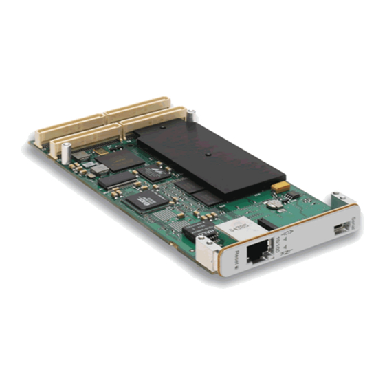
- Page 1 User’s Manual from Emerson Network Power ™ Embedded Computing Pm8560: Octal E1/T1/J1 Line Interface PTMC October 2007...
- Page 2 EMERSON DOES NOT ASSUME ANY LIABILITY ARISING OUT OF USE OR OTHER APPLICATION OF ANY PRODUCT, CIRCUIT, OR PROGRAM DESCRIBED HEREIN. This document does not convey any license under Emerson patents or the rights of others.
- Page 3 Emerson Network Power. Caution: For applications where the Pm8560 is provided without a front panel, or where the front panel has been removed, your system chassis/enclosure must provide the required electromagnetic interference (EMI) shielding to maintain EMC compliance.
- Page 4 EMC Directive and RTTE Directive. We have an inter- nal production control system that ensures compliance between the manufactured products and the technical documentation. Bill Fleury Compliance Engineer Issue date: October 10, 2007 Pm8560 User’s Manual 10006609-03...
-
Page 5: Table Of Contents
6 TDM Interface Pm8560 Setup ..... 2-5 Power Requirements ... . . 2-6 TDM Framer and Line Interface . - Page 6 Ethernet Connector ....9-2 nm ......11-12 Pm8560 User’s Manual 10006609-03...
- Page 7 ..... . .11-18 coninfo ..... . .11-18 10006609-03 Pm8560 User’s Manual...
- Page 8 Contents (continued) Pm8560 User’s Manual 10006609-03...
- Page 9 Installing the Pm8560 on the Baseboard ........
- Page 10 (blank page) viii Pm8560 User’s Manual 10006609-03...
- Page 11 Interrupt Connections for Pm8560 ........
- Page 12 (blank page) Pm8560 User’s Manual 10006609-03...
- Page 13 Register 8-31: SPD Write Recovery Time (SPDWRT), 0x80 ........8-25 Register 8-32: SPD Internal Write-to-Read Command Delay (SPDIWR), 0x84 ....8-25 10006609-03 Pm8560 User’s Manual...
- Page 14 (blank page) Pm8560 User’s Manual 10006609-03...
-
Page 15: Overview
(ECC). DDR interface operating speed is 133 MHz when the processor core is at 800 MHz. Flash: The Pm8560 is capable of booting from either an 8-bit, 32-pin PLCC ROM socket on the Development Mezzanine Card (DMC), or from the 16-bit on-card soldered flash (default) region. -
Page 16: Functional Overview
Table 1-3 mation. Transition Model (TM): TMcSpanP8E provides four or eight rear long- or short-haul T1 or E1 links. See the Emerson TMcSpanP8E User’s Manual for more information. Development Mezzanine Card: An optional Development Mezzanine Card (DMC) is available for software development. -
Page 17: Figure 1-1: General System Block Diagram
Figure 1-1: General System Block Diagram The Pm8560 monitor can boot from either the DMC socketed PLCC device or the soldered flash (default). Based on the DMC jumper JP2 (see “DMC Jumpers and LEDs”), either the DMC socket or the soldered flash is mapped to the boot bank at FFF0,0000 . -
Page 18: Memeory Map
Overview: Functional Overview Figure 1-2: Memeory Map Pm8560 User’s Manual 10006609-03... -
Page 19: Address Summary
E808,0034 Miscellaneous Control (MISC) 8-11 E808,0030 Boot Device Failover Mechanism (BDFM) E808,002C PCI Status (PSR) E808,0028 PCI Reset Out Enable (PROE) E808,0024 Reset Command (RCR) E808,0020 Reset Event (RER) E808,001C LED (LEDR) E808,0018 Jumper Setting (JSR) 10006609-03 Pm8560 User’s Manual... -
Page 20: Additional Information
SR-332, Issue 1, Reliability Prediction for Electronic Equipment at 30 Product Certification The Pm8560 hardware has been tested to comply with various safety, immunity, and emis- sions requirements as specified by the Federal Communications Commission (FCC), Under- writers Laboratories (UL) Inc., and others. The following table summarizes this compliance:... -
Page 21: Rohs Compliance
Pm8560 hardware’s ability to comply with any of the stated specifications. The UL web site at ul.com has a list of Emerson’s UL certifications. To find the list, search in the online certifications directory using Emerson’s UL file number, E190079. There is a list for products distributed in the United States, as well as a list for products shipped to Can- ada. -
Page 22: Technical References
Radix 2 and 16: Hexadecimal numbers end with a subscript 16. Binary numbers are shown with a subscript 2. Technical References Further information on basic operation and programming of the Pm8560 components can be found in the following documents: Table 1-3: Technical References... - Page 23 (Electronic Industries Association, October 1997) http://www.eia.org Timing M41T00 Serial Access TIMEKEEPER® Data Sheet (ST® Microelectronics June 2004) http://www.st.com/ T1/E1/OC3 System Synchronizer Data Sheet (Zarlink™ Semiconductor, Inc. MT9045 February 2005) http://www.zarlink.com/ Baseboard Emerson Katana752i User’s Manual (Emerson Network Power #10006024-xx) http://www.emersonembeddedcomputing.com/ 10006609-03 Pm8560 User’s Manual...
- Page 24 Overview: Additional Information Device / Interface: Document: (continued) Transition Emerson TMcSpanP8E User’s Manual Module Emerson Network Power #10005363-xx) http://www.emersonembeddedcomputing.com/ 1. Frequently, the most current information regarding addenda/errata for specific documents may be found on the corresponding web site. 1-10 Pm8560 User’s Manual...
-
Page 25: Setup
Do not place the board on metal or other conductive surfaces. PM8560 CIRCUIT BOARD The Pm8560 circuit board is a PTMC module assembly. It uses a 14-layer printed circuit board with the following dimensions: Table 2-1:... -
Page 26: Pm8560 Circuit Board
Setup: Pm8560 Circuit Board Figure 2-1: Component Map, Top (Rev. 03) Mini-B RJ45 Transformer SDRAM SDRAM RN10 RN11 IDT82P2288 QUAD Framer SDRAM SDRAM RN12 RN13 RN14 RN15 RN16 RN17 RN18 RN19 RN20 RN21 RN22 RN23 RN24 RN25 RN26 RN27 RN28... -
Page 27: Figure 2-2: Component Map, Bottom (Rev. 01)
Setup: Pm8560 Circuit Board Figure 2-2: Component Map, Bottom (Rev. 01) 10000000-00-xx C102 708- RN36 C106 C105 C103 C113 C112 C115 C114 C116 C117 Flash RN54 RN52 RN51 RN50 RN49 RN48 RN47 RN46 RN45 RN44 RN43 RN42 RN41 RN40 RN39... -
Page 28: Figure 2-3: Led And Switch Locations, Top
Setup: Pm8560 Circuit Board Figure 2-3: LED and Switch Locations, Top Pm8560 User’s Manual 10006609-03... -
Page 29: Connectors
(EMI) shielding to maintain EMC compliance. PM8560 SETUP You need the following items to set up and check the operation of the Emerson Pm8560: ❐ Emerson Katana752i baseboard and TMcSpanP8E read transition module (RTM) ❐ cPCI chassis and power supply ❐... -
Page 30: Pm8560 Setup
The Pm8560 is not a Hot Swap compliant module. Removing the Pm8560 while power is applied, may damage the board. To remove a Pm8560 from a cPCI rack, remove the carrier card first, then remove the Pm8560 from the carrier card. -
Page 31: System Jtag Chain
Reset Diagram System JTAG Chain The Pm8560 has a dynamically structured JTAG chain that adds valuable debugging fea- tures. JTAG type boundary scan testing can be performed on the major board devices through the PMC connectors, P11 and P12. A quick switch isolates the CPLD and MPC8560 from the rest of the JTAG chain when a DMC module is installed. -
Page 32: Installation
System JTAG Diagram Installation The Pm8560 module may be installed in any expansion slot on a baseboard. To attach the module to your baseboard, follow these steps: Line up the P11 through P14 connectors and the keying holes with the PMC connectors J11 through J14 and the keying pin on the baseboard. -
Page 33: Troubleshooting
Installing the Pm8560 on the Baseboard TROUBLESHOOTING In case of difficulty, use this checklist: ❐ Be sure the Pm8560 circuit board is seated firmly on the baseboard and the baseboard is seated in the carrier. ❐ Be sure the system is not overheating. -
Page 34: Technical Support
Setup: Troubleshooting Technical Support If you plan to return the board to Emerson Network Power for service, visit http://www.emersonembeddedcomputing.com/contact/postsalessupport.html on the internet or send E-mail to support@artesyncp.com. Have the following information handy: • Pm8560 serial number and product ID (see Fig. -
Page 35: Product Repair
Setup: Troubleshooting Product Repair If you plan to return the board to Emerson Network Power for service, visit http://www.emersonembeddedcomputing.com/contact/productrepair.html on the inter- net or send E-mail to serviceinfo@artesyncp.com to obtain a Return Merchandise Authori- zation (RMA) number. We will ask you to list which items you are returning and the board serial number, plus your purchase order number and billing information if your Pm8560 hardware is out of warranty. - Page 36 Setup: Troubleshooting 2-12 Pm8560 User’s Manual 10006609-03...
-
Page 37: Central Processing Unit
Section 3 Central Processing Unit This chapter is an overview of the processor logic on the Pm8560. It includes information on the CPU, exception handling, and the I/O parallel port pin assignments. The Pm8560 uses a Freescale MPC8560 PowerQUICC III™ microprocessor. For more detailed informa- tion, refer to the MPC8560 PowerQuicc III Integrated Communications Processor Reference Manual. -
Page 38: Mpc8560 Functions
For more detailed information, reference the Freescale application note Migrating from PowerQUICC II to PowerQUICC III. MPC8560 FUNCTIONS The MPC8560 provides the following functions on the Pm8560 module. System functions include: • DDR SDRAM memory controller • Chip select generation for the framers and PLD •... -
Page 39: Microprocessor Core (E500)
The Machine State register (MSR) configures the state of the MPC8560. On initial power-up of the Pm8560, most of the MSR bits are cleared. Refer to the MPC8560 PowerQuicc III Inte- grated Communications Processor Reference Manual for more detailed descriptions of the individual bit fields. -
Page 40: Communications Processor Module
Interrupt levels may be programmed for logic low or negative edge assertion. The interrupt controller combines all the sources into a single interrupt output to the Programmable Interrupt Con- troller (PIC). Figure 3-1: CPM Interrupt Structure Pm8560 User’s Manual 10006609-03... -
Page 41: Internal Interrupt Sources
Asserted by MT9045 when secondary reference is out of capture range SS_HOLDOVER PC11 MT9045 system synchronizer holdover mode SS_MODE_SELECT1 PC12 MT9045 system synchronizer mode/control select 1 SS_MODE_SELECT2 PC13 MT9045 system synchronizer mode/control select 2 no connect PC14 10006609-03 Pm8560 User’s Manual... -
Page 42: Mpc8560 Cpm Port Pin Assignment
MPC8560 CPM Port Pin Assignment MPC8560 CPM PORT PIN ASSIGNMENT Several signals are available on each of the MPC8560 CPM port pins, lists the Table 3-3 MPC8560 signals used on the Pm8560 module Table 3-3: MPC8560 Port Pin Assignments MPC8560 Pin:... - Page 43 TDM port 6 transmit data reserved reserved reserved reserved reserved SS_FASTLOCK MT9045 system synchronizer fast lock mode SS_PPC MT9045 system synchronizer phase continuity control SS_TCLR MT9045 system synchronizer time interval error (TIE) circuit reset SS_LOCK MT9045 system synchronizer lock indicator 10006609-03 Pm8560 User’s Manual...
- Page 44 TDM2_TSYNC TDM port 2 transmit synchronization PD12 TDM2_RXD TDM port 2 receive data PD13 TDM2_TXD TDM port 2 transmit data PD14 P11_SCL connector P11 serial clock PD15 P11_SDA connector P11 serial data PD16 reserved PD17 reserved Pm8560 User’s Manual 10006609-03...
-
Page 45: Mpc8560 Peripheral Modules
The MPC8560 memory controller functions as a chip select (CS) generator to access on- board memory devices, saving the board’s area which results in reduced cost, power con- sumption, and increased flexibility. lists the chip selects for the Pm8560 module. Table 3-4 10006609-03... -
Page 46: Processor Reset And Clocking Signals
8 kilobytes of RAM (with a base address of 0000,0000 ) or flash (with a base address of E000,0000 ). An unassigned vector position may be used to point to an error routine or for code or data storage. 3-10 Pm8560 User’s Manual 10006609-03... -
Page 47: On-Card Memory
Section 4 On-Card Memory This chapter describes the various memory devices on the Pm8560. These include: • 32 megabytes soldered flash memory • 512 kilobytes socketed flash on the DMC • 256 to 512 megabytes DDR SDRAM devices • three serial EEPROMs •... -
Page 48: Serial Eeproms
C SROM for storing non-volatile information such as board, monitor, operating system configurations, as well as information specific to user application. All Emerson-specific data is stored in the upper two kilobytes of the device. The remainder of the device is available for user application. -
Page 49: Double Data Rate Sdram
On-Card Memory: Double Data Rate SDRAM DOUBLE DATA RATE SDRAM The Pm8560 supports up to 512 megabytes of DDR SDRAM for data storage. On-card SDRAM occupies physical addresses starting at 0000,0000 . The double data rate archi- tecture is designed to enhance performance especially in high-speed operation. The DDR SDRAM interface operates at 133 MHz when the processor core is at 800 MHz. - Page 50 (continued) A12-A7 (12:7) Operating Mode ‘000000’ Normal operation A6-A4 (6:4) CAS Latency ‘010’ Data valid two cycles after CAS asserted A3 (3) Burst Type ‘0’ Sequential burst A2-A0 (2:0) Burst Length ‘010’ Four word burst length Pm8560 User’s Manual 10006609-03...
-
Page 51: Serial I/O
Section 5 Serial I/O This chapter describes the Pm8560 serial ports and baud rate generators. SERIAL PORTS EIA-232 Serial Port: The serial port from the MPC8560 is available at the front panel, connector P14, and the DMC; or connector P13 when a CT bus is present. This serial port is for boot flash program- ming, initial setup, and debug. -
Page 52: Figure 5-1: Serial Cable Assembly (Emerson Part Number C00003555-Xx)
Serial I/O: Baud Rate Selection Figure 5-1: Serial Cable Assembly (Emerson part number C00003555-xx) Caution: The USB mini-B cable connection to P17 does not have a locking mechanism. Pulling on the cable may result in a disconnection. Table 5-2: Serial Cable Wiring Assignments... -
Page 53: Baud Rate Selection
BRGC5-8 registers start at physical address space FDF9,15F0 and BRGC1-4 regis- ters start at physical address space FDF9,19F0 . For more detailed information on these registers, refer to the MPC8560 PowerQuicc III Integrated Communications Processor Reference Manual. 10006609-03 Pm8560 User’s Manual... - Page 54 Serial I/O: Baud Rate Selection Pm8560 User’s Manual 10006609-03...
-
Page 55: Tdm Interface
• Three signals for the transmitter (TDMx TXD, TDMx TCLK, TDMx TSYNC) • Three for the receiver (TDMx RXD, TDMx RCLK, TDMx RSYNC) TDM FRAMER AND LINE INTERFACE The Pm8560 module includes support for eight links using one IDT82P2288 octal T1/E1/J1 (long haul/short haul) framer and line interface (LIU). Framer •... -
Page 56: Framer Analog Interfaces
Specific configurations also use the MT9045 System Synchronizer device. Setting up the MT9045 in the desired mode and frequency requires two steps: Drive the correct Pm8560 CPM port pins (PC5, PC6, PC7, PC12, PC13) as defined in Table 3-3 Set the appropriate registers in the MT9045 System Synchronizer Control register (SSCR) on page 8-15. - Page 57 • If line is 1.544 MHz, then system is 1.544 MHz; if line is 2.048 MHz, then system is 2.048 • The MT9045 is not installed • There is no CT bus clocking • Recovered RCLK and RSYNC used as basis of TCLK and TSYNC 10006609-03 Pm8560 User’s Manual...
-
Page 58: Signal Definitions
Receive Side System Clock (links 1-8) In receive clock master mode, the RSCKn pins out- put a 1.544 MHz (T1/J1)/2.048 MHz (E1) clock. In receive clock slave mode, the RSCKn pins input a 1.544 MHz (T1/J1 only), 2.048 or 4.096 MHz clock. Pm8560 User’s Manual 10006609-03... -
Page 59: Framer Waveform Shape
Table 64, Scale 0x2C Table 63, Scale 0x26 Note: Scale values for other Emerson RTMs are available upon request, contact Technical Support. FRAMER INTERRUPT MECHANISM Special events in the framer are indicated by means of a single interrupt output (INT* pin T11) with programmable characteristics (open drain). -
Page 60: Rear Panel I/O Connector P14
TTIP3 TRING3 no connect TM_ID0 RTIP3 RRING3 TM_ID2 no connect TTIP4 TRING4 TM_ID3 no connect no connect no connect RTIP4 RRING4 TTIP5 TRING5 RTIP5 RRING5 TTIP6 TRING6 RTIP6 RRING6 TTIP7 TRING7 RTIP7 RRING7 TTIP8 TRING8 Pm8560 User’s Manual 10006609-03... - Page 61 TDM Interface: Rear Panel I/O Connector P14 P14 Pin: Signal: P14 Pin: Signal: (continued) RTIP8 RRING8 10006609-03 Pm8560 User’s Manual...
- Page 62 TDM Interface: Rear Panel I/O Connector P14 Pm8560 User’s Manual 10006609-03...
-
Page 63: Pci Bus Interface
Section 7 PCI Bus Interface The Pm8560 module design complies with the Peripheral Component Interconnect (PCI) bus interface standard and the associated PCI Mezzanine Card (PMC) mechanical interface standard. The Freescale MPC8560 PowerQUICC III microprocessor controller provides the bridge between the PCI interface and the MPC8560 OCeaN switch fabric. For more detailed information, refer to the MPC8560 PowerQuicc III Integrated Communications Processor Refer- ence Manual. -
Page 64: Mpc8560 Pci Memory Map
PCI bus (addr0). The registers are located on the PCI local bus after the SDRAM image (for example, 0+<pci_memsize>+<register offset>). Non-Mon- arch mode mapping is set by the baseboard that the Pm8560 is installed on. For more infor- mation on these registers, refer to the MPC8560 PowerQuicc III Integrated Communications Processor Reference Manual. -
Page 65: Monitor Display
0x09 (9d) 60-69 96-105 Serial number in ASCII “708A-XXXXX” 6A-6B 106-107 Read-only vendor-specific keyword “V0” (vendor-specific field 0=Emerson Pm8560 PCBA number) Length of vendor-specific “V0” data 0x0B (11d) field 6D-77 109-119 Vendor-specific “V0” data field in “1000XXXX-YY” ASCII 78-79 120-121 Read-only checksum keyword “RV”... -
Page 66: Accessing The Serial Eeprom Vpd
PCI Configuration and Status Register Base Address register (PCSRBAR) 32-Bit Memory Base Address register 64-Bit Low Memory Base Address register 64-Bit High Memory Base Address register 64-Bit Low Memory Base Address register 64-Bit High Memory Base Address register reserved Pm8560 User’s Manual 10006609-03... -
Page 67: Power-On Reset Modes
Host Agent Agent configuration lock Monarch Mode The Pm8560 supports the Monarch features of the Processor PMC (ANSI/VITA 32-2003) specification (See Technical References in ). The PMC_MONARCH signal is con- Table 1-3 nected to the CPLD and is read through the CPLD PCI Status register (see PCI Status register 10006609-03 Pm8560 User’s Manual... -
Page 68: Pci Interrupts
8-9). In order to operate as described in the Processor PMC specification, the software must read this status to determine if the monarch features of the Pm8560 should be enabled. If the monarch signal is low, then the software should perform PCI bus enumera- tion and interrupt handling. -
Page 69: Table 7-4: P11, P12, And P13 Connector Pin Assignments
PCI-reserved 3.3 V no connect PCI-reserved SERR* NETREF1 CBE1* CT_C8_B V(I/O) AD14 AD15 AD13 no connect AD12 M66EN no connect AD11 AD10 no connect no connect 3.3 V no connect CBE0* no connect no connect 10006609-03 Pm8560 User’s Manual... -
Page 70: Pci Bus Control Signals
Each master has its own GNT*. IDSEL: INITIALIZATION DEVICE SELECT input signal acts as a chip select during configuration read and write transactions. INTA*-INTD*: INITIALIZATION DEVICE SELECT input signal acts as a chip select during configuration read and write transactions. Pm8560 User’s Manual 10006609-03... - Page 71 TRDY*: TARGET READY is a sustained tri-state signal that indicates the target’s ability to complete the current data phase of the transaction. TRST*: TEST RESET (JTAG) is the asynchronous reset for the JTAG controller (input sighal). 10006609-03 Pm8560 User’s Manual...
- Page 72 PCI Bus Interface: PMC Connector Pin Assignments 7-10 Pm8560 User’s Manual 10006609-03...
-
Page 73: Programmable Logic Device
Section 8 Programmable Logic Device The Pm8560 uses a Programmable Logic Device (PLD) to provide control logic for the local bus. The PLD implements various registers for product identification, board configuration, reset, clocking, and Serial Presence Detect (SPD). This chapter describes the PLD registers on the Pm8560. -
Page 74: Pld Register Summary
SPDIWR SPD Internal Write-to-Read Command Delay 8-32 Product ID This read-only register identifies the board as Pm8560, and is used for PLD coding. Register 8-1: Product ID (PIDR), 0x00 PID7-0: The current Product ID number is 0x00. Future ID numbers may include 0x01, 0x02, or 0x03. -
Page 75: Pld Version
PMC RSTOUT Baseboard writes the MPC8560 RCR via PCI to cause a SW HRESET The Pm8560 resets and the processor samples the new PLL configuration values The baseboard will not reset (because the PROE prevented the PMC RSTOUT) The baseboard must re-enumerate and initialize the Pm8560 Caution: Do not attempt to over-clock the processor. -
Page 76: Hardware Configuration 1
0 ECC is not present 1 ECC is present DDR1-0: DDR memory Density 00 256 megabit devices (default) 01 256 megabit devices 10 Reserved 11 Reserved DDRR: DDR memory Rows 0 One bank (default) 1 Two banks Pm8560 User’s Manual 10006609-03... -
Page 77: Jumper Settings
ISROM: Ignore SROM displays whether SROM will be initialized. When the DMC is installed on the Pm8560, and DMC shunt JP3 [5:6] is installed, the MPC8560 Init EEPROM (on the Pm8560) is not used for initialization. 0 No SROM, Pm8560 EEPROM is used for initialization (default) -
Page 78: Reset Event
Set to 1 when a COP header soft reset (SRESET) has occurred. COPHR: COP Hard Reset Set to 1 when a COP header hard reset (HRESET) has occurred. PAYRST: Payload Reset Set to 1 when a payload reset has occurred. reserved: Default is 00 Pm8560 User’s Manual 10006609-03... -
Page 79: Reset Command
MT9045 System Synchronizer Reset 0 No reset (default) 1 Reset PMC Reset Out PMCRO: This bit allows software to reset the Pm8560 based on the values set in PROE bits [5:0]. 0 No reset (default) 1 Reset I2CR: C Reset This will reset both I C ports. -
Page 80: Pci Reset Out Enable
1 Enable PCI Status The Pm8560 provides a register for status and control of enumeration and monarch status. In a Monarch system, the PCIE field is readable to indicate that other boards in the system are ready for enumeration. In a non-Monarch system, the PCIE field is writeable to indicate the Pm8560 is ready for enumeration. -
Page 81: Boot Device Failover Mechanism
The read-only Boot Device Failover Mechanism (BDFM) register is only functional when the DMC is not installed on the Pm8560. This register enables the Pm8560 to recover from monitor corruption by booting from a redundant copy in another flash device. The mecha- nism relies on the processor’s internal watchdog to expire when corrupted code fails to... - Page 82 This indicates that the image in the default device was defective, the MPC8560 watchdog timer expired, and the next device was tried. This bit is only cleared after the Pm8560 has been power cycled. 0 Boot failover has not occurred...
-
Page 83: Miscellaneous Control
0 Selects the P13 serial port 1 Selects the front panel, P14, and DMC serial port SIOCON: Serial I/O Control 0 Combine received data from both ports 1 Software selects the serial I/O port (default) 8-11 10006609-03 Pm8560 User’s Manual... -
Page 84: Ct Bus Status
0x40 through 0x5c. This dia- Fig. 8-2 gram is a tool designed to help configure the TDM interfaces. Refer to the specific CPLD register for more detail. 8-12 Pm8560 User’s Manual 10006609-03... -
Page 85: Figure 8-2: Clock And Sync Registers Diagram
Programmable Logic Device: Clock and Sync Registers Figure 8-2: Clock and Sync Registers Diagram 8-13 10006609-03 Pm8560 User’s Manual... -
Page 86: Netref Control
CT bus C8B 8.192 MHz clock 0 Disable 1 Enable CTC8A: CT bus C8A 8.192 MHz clock 0 Disable 1 Enable MT1.5: MT9045 1.544 MHz clock 0 Disable 1 Enabled MT2.0: MT9045 2.048 MHz clock 0 Disable 1 Enable 8-14 Pm8560 User’s Manual 10006609-03... -
Page 87: Mt9045 System Synchronizer Control
SS_SECEN: System Synchronizer Secondary Enable 0 Disables these buffers when the MT9045 functionality is not used (ensures they are negated) 1 Enables secondary clock source to be driven to the MT9045 reserved: Default is 00 8-15 10006609-03 Pm8560 User’s Manual... -
Page 88: Sync Source
CT_FA 0 Disable 1 Enable CTFB: CT_FB 0 Disable 1 Enable MT8K: MT4095 8 KHz clock 0 Disable 1 Enable PRIM8K: Primary MUX divide to 8 KHz 0 Disable 1 Enable reserved: Default is 0 8-16 Pm8560 User’s Manual 10006609-03... -
Page 89: Primary Clock Source
0 Disable 1 Enable FR2.0: Framer 2.048 MHz clock 0 Disable 1 Enable CTC8A: CT bus C8A 2.048 MHz clock 0 Disable 1 Enable CTC8B: CT bus C8B 2.048 MHz clock 0 Disable 1 Enable 8-17 10006609-03 Pm8560 User’s Manual... -
Page 90: Secondary Clock Source
0 Disable 1 Enable FR2.0: Framer 2.048 MHz clock 0 Disable 1 Enable CTC8A: CT bus C8A 2.048 MHz clock 0 Disable 1 Enable CTC8B: CT bus C8B 2.048 MHz clock 0 Disable 1 Enable 8-18 Pm8560 User’s Manual 10006609-03... -
Page 91: Tclk Source
MT2.0: MT9045 2.048 MHz clock 0 Disable 1 Enable PRIM: Primary MUX 0 Disable 1 Enable SECM: Secondary MUX 0 Disable 1 Enable RCLK Source Register 8-22: RCLK Source (RCSR), 0x5C RCLKM reserved TCON RCON 8-19 10006609-03 Pm8560 User’s Manual... -
Page 92: Serial Presence Detect (Spd) Registers
Column Addressing of the on-board DDR SDRAM 000 8-column bits 001 9-column bits 010 10-column bits 011 11-column bits 100—111 Reserved NROWS: Number of physical banks of the on-board DDR SDRAM 0 1 row 1 2 rows 8-20 Pm8560 User’s Manual 10006609-03... -
Page 93: Cas Latency Refresh
Refresh Rate for the on-board DDR SDRAM 000 Reserved 001 3.9 msec refresh period 010—111 Reserved SDRAM Cycle Time for CAS Latency Register 8-25: SPD SDRAM Cycle Time for CAS Latency (SPDCT), 0x68 CYCTWHNS CYCTTENS 8-21 10006609-03 Pm8560 User’s Manual... -
Page 94: Minimum Row Precharge Time
111110 62 ns 111111 63 ns TRPQTRNS: Minimum Row Precharge Time for the on-board DDR SDRAM (quarter nanosecond granu- larity) 00 + 0 ns 01 + .25 ns 10 + .50 ns 11 + .75 ns 8-22 Pm8560 User’s Manual 10006609-03... -
Page 95: Minimum Row Delay Between Activations
TRCDWHNS: Minimum delay required between assertions of RAS and CAS for the on-board DDR SDRAM (whole nanosecond granularity) 000000 Reserved 000001 1 ns 000010 2 ns 000011 3 ns 111110 62 ns 111111 63 ns 8-23 10006609-03 Pm8560 User’s Manual... -
Page 96: Minimum Active-To-Precharge
SPD Minimum Auto-Refresh to Active/Auto-Refresh (SPDMAA), 0x7C MARTAR MARTAR: Minimum Auto-Refresh To Active/Auto-Refresh command period for the on-board DDR SDRAM 00000000 (0x00) Reserved 00000001 (0x01) 1 ns 00000010 (0x02) 2 ns 00000011 (0x03) 3 ns 01111111 (0x7F) 127 ns 8-24 Pm8560 User’s Manual 10006609-03... -
Page 97: Write Recovery Time
Register 8-32: SPD Internal Write-to-Read Command Delay (SPDIWR), 0x84 WTRWHNS WTRQTRNS WTRWHNS: Internal Write-to-Read command delay for the on-board DDR SDRAM (whole nanosecond granularity) 000000 Reserved 000001 1 ns 000010 2 ns 000011 3 ns 8-25 10006609-03 Pm8560 User’s Manual... - Page 98 111110 62 ns 111111 63 ns WRTQTRNS: Internal Write-to-Read command delay for the on-board DDR SDRAM (quarter nanosecond granularity) 00 + 0 ns 01 + .25 ns 10 + .50 ns 11 + .75 ns 8-26 Pm8560 User’s Manual 10006609-03...
-
Page 99: Ethernet Interfaces
Embedded Computing by IEEE. The lower 24 bits are defined by Emerson for identification of each of our products. The Ethernet address for the Pm8560 is a binary number referenced as 12 hexadecimal dig- its separated into pairs, with each pair representing eight bits. The address assigned to the... -
Page 100: Ethernet Connector
The last pair of hex numbers correspond to the following formula: n — 1000, where n is the unique serial number assigned to each board. MAC[15:0] is the serial number plus 0x00 (port 0) or 0x80 (port 2). For example, if the serial number of a Pm8560 is 1032, the calcu- lated value is 32 (20 ), and the port addresses are: •... -
Page 101: Development Mezzanine Card
The Development Mezzanine Card (DMC) is an optional plug-on card mounted on the back of the Pm8560 board. This chapter describes the physical layout of the DMC, the setup pro- cess, and how to check for proper operation once the board has been installed. The DMC facilitates hardware and software development by providing access to: •... -
Page 102: Connectors
CONNECTORS The DMC has the following connectors: This 80-pin PCB-to-PCB female connector on the bottom side of the DMC routes memory, PLD, and CPU signals from the Pm8560 to the DMC for development use. See Table 10-2 the pin assignments. -
Page 103: P1 Connector Pin Assignments
LA11 LA10 FLASH_D0 FLASH_D1 FLASH_D2 FLASH_D3 FLASH_D4 FLASH_D5 FLASH_D6 FLASH_D7 SCC1_RS232_TX SCC1_RS232_RX 3.3 V 3.3 V 3.3 V CPU_TCK no connect no connect no connect no connect no connect no connect no connect reserved BOOT_FROM_SOCKET 10-3 10006609-03 Pm8560 User’s Manual... - Page 104 Check Stop Out is an input to DMC used by the debug header. CPLD_TDI: PLD Test Data In is part of the PLD JTAG interface (analog). CPLD_TMS: PLD Test Mode Select is an output from DMC and part of PLD JTAG interface. 10-4 Pm8560 User’s Manual 10006609-03...
-
Page 105: P2 Eia-232 Interface
PLD Test Data Out is an input to DMC and part of PLD JTAG interface. CPLD_TDO: DMC_PD*/DMC_PD: DMC Presence Detect is an output from DMC and indicates to the Pm8560 that the DMC is installed. P2 EIA-232 Interface Use the standard serial cable, Emerson part number C0003555-00, to access connector P2. -
Page 106: P4 Jtag Chain Header
CPLD_TDI Ground CPLD_TCK: Test Clock Input—this is the clock input to the boundary scan test (BST) circuitry. Some oper- ations occur at the rising edge, while others occur at the falling edge. 10-6 Pm8560 User’s Manual 10006609-03... -
Page 107: Dmc Jumpers And Leds
A shunt on pins 3 and 4 selects the 8-bit ROM socket as the boot device. So in order for the socket to provide boot code, the DMC must be seated on the Pm8560 and the boot shunt must be in place. If the shunt is not installed, the boot device is Pm8560 flash bank 1. JP3: Pins 5 and 6 are the serial ROM configuration jumper. -
Page 108: Dmc Setup
Development Mezzanine Card: DMC Setup DMC SETUP You need the following items to set up and check the operation of the Emerson DMC: ❐ A compatible PTMC board, such as the Emerson Pm8560 ❐ cPCI chassis and power supply ❐ Computer terminal Save the antistatic bag and box for future shipping or storage. -
Page 109: Troubleshooting
DMC Location on Pm8560 TROUBLESHOOTING In case of difficulty, use this checklist: ❐ Be sure the DMC is seated firmly on the Pm8560 and that the PTMC host is seated firmly in the card cage. ❐ Verify the boot jumper settings (see Fig. -
Page 110: Technical Support
Development Mezzanine Card: Troubleshooting Technical Support If you plan to return the board to Emerson Network Power for service, visit http://www.emersonembeddedcomputing.com/contact/postsalessupport.html on the internet or send E-mail to support@artesyncp.com. Have the following information handy: • DMC serial number, product ID (see Fig. - Page 111 Development Mezzanine Card: Troubleshooting Emerson Network Power, Embedded Computing Test and Repair Services Department 8310 Excelsior Drive Madison, WI 53717 RMA #____________ Put the RMA number on the outside of the package so we can handle your problem effi- ciently. Our service department cannot accept material received without an RMA number.
- Page 112 Development Mezzanine Card: Troubleshooting 10-12 Pm8560 User’s Manual 10006609-03...
-
Page 113: Monitor
After entering a command, re-execute it simply by pressing the ENTER or RETURN key. Auto-Repeat: TFTP Boot: Use the TFTP protocol to load application images via Ethernet into the Pm8560’s memory. Auto-Boot: Store specific boot commands in the environment to be executed automatically after reset. -
Page 114: Basic Operation
Figure 11-1: Example Monitor Start-up Display BASIC OPERATION The Pm8560 monitor performs various configuration tasks upon power-up or reset. This section describes the monitor operation during initialization of the Pm8560 board. The flowchart (see ) illustrates the power-up and global reset sequence (bold text indi- Fig. - Page 115 C bus (SMB bus) Configure 8560 I/O ports Set debug LED 0011 Set debug LED 0110 Turn off debug LEDs Initialize 8560 memory Initialize console routines in Initialize I C bus #1 controller Main loop 11-3 10006609-03 Pm8560 User’s Manual...
-
Page 116: Post Diagnostic Results
Any writes to these areas can cause unpredictable operation of the monitor. Updating the Monitor A new feature of the Pm8560 is the ability to boot from a duplicate copy of the monitor located in another flash bank. To take advantage of this feature, make sure both soldered flash banks have the most current version of the monitor. -
Page 117: Table 11-2: Monitor Address Per Flash Size
If it is necessary to manually update the monitor, follow steps 3 through 5 to update flash bank 0. Unprotect the flash: Pm8560 (1.4) => protect off bank 0 Erase the monitor region of soldered flash (see Table 11-2 Pm8560 (1.4) => erase e1f80000 e1ffffff Program the monitor into soldered flash bank 0: Pm8560 (1.4) =>... -
Page 118: Boot Redirect And Monitor Recovery (Watchdog)
Basic Operation Boot Redirect and Monitor Recovery (Watchdog) The PLD initiates a countdown to reset the Pm8560 and boot from an alternate location within .5 second of power-up. The monitor disables the PLD watchdog (see “Boot Device Failover Mechanism” on page 8-9) and enables its own software watchdog that will activate at approximately 10 second intervals. -
Page 119: Resetting Environment Variables
Pm8560 (1.4) => saveenv MONITOR COMMAND REFERENCE This section describes the syntax and typographic conventions for the Pm8560 monitor commands. Subsequent sections in this chapter describe individual commands, which fall into the following categories: boot, memory, flash, environment variables, test, and other commands. -
Page 120: Command Help
The host board finally writes 0x596F4F6B (character string “YoOk”) to MagicLoc to show that the application is ready for the target. The target writes value 0x42796521 (character string “Bye!”) to MagicLoc to show that the application was found. If necessary, the target then updates its memory-resident loadaddr 11-8 Pm8560 User’s Manual 10006609-03... -
Page 121: Bootd
Write image to flash and update NVRAM. bootv <primary | secondary> write <source> <dest> <size> Update NVRAM based on image already in flash. bootv <primary | secondary> update <source> <size> Check validity of images in flash. bootv <primary | secondary> check 11-9 10006609-03 Pm8560 User’s Manual... -
Page 122: Dhcp
If you do not specify a flag, memory commands default to 32-bit long words. Numeric arguments are in hexadecimal. The cmp command compares count objects between addr1 and addr2. Any differences are displayed on the console display. 11-10 Pm8560 User’s Manual 10006609-03... -
Page 123: Find
00080000: ffff ffff ffff ffff ffff ffff ffff ffff ....00080010: ffff ffff ffff ffff ffff ffff ffff ffff ....00080020: ffff ffff ffff ffff ffff ffff ffff ffff ....00080030: ffff ffff ffff ffff ffff ffff ffff ffff ....11-11 10006609-03 Pm8560 User’s Manual... - Page 124 00080000: abbaabba abbaffff ffffffff ffffffff ....00080010: ffffffff ffffffff ffffffff ffffffff ....00080020: ffffffff ffffffff ffffffff ffffffff ....00080030: ffffffff ffffffff ffffffff ffffffff ....00080040: ffffffff ffffffff ffffffff ffffffff ....00080050: ffffffff ffffffff ffffffff ffffffff ....11-12 Pm8560 User’s Manual 10006609-03...
-
Page 125: Flash Commands
....FLASH COMMANDS The flash commands affect the StrataFlash devices on the Pm8560 circuit board. There is one flash bank on the Pm8560 board. The following flash commands access the individual flash bank as flash bank 0. To access the individual sectors within each flash bank, the sector numbers start at 0 and end at one less than the total number of sectors in the bank. -
Page 126: Protect
[ .0, .1, .2 ] count iloop The iloop command reads in an infinite loop on the specified address range. Definition: iloop chip address [ .0, .1, .2 ] [ # of objects ] 11-14 Pm8560 User’s Manual 10006609-03... -
Page 127: Imd
Definition: imw chip address [ .0, .1, .2 ] value [ count ] The inm command modifies I C memory, reads it, and keeps the address. Definition: inm chip address [ .0, .1, .2 ] 11-15 10006609-03 Pm8560 User’s Manual... -
Page 128: Iprobe
The setenv command adds new environment variables, sets the values of existing environ- ment variables, and deletes unwanted environment variables. Definition: Set the environment variable name to value or adds the new variable name and value to the environment. setenv name value 11-16 Pm8560 User’s Manual 10006609-03... -
Page 129: Srom_Wp
[ .b, .w, .l ] base_addr [ top_addr ] test_watchdog The test_watchdog command disables interrupts and remains in an infinite loop. This indi- cates when the first and second watchdogs occur. The second watchdog resets the board. Definition: test_watchdog 11-17 10006609-03 Pm8560 User’s Manual... -
Page 130: Other Commands
Monitor: Other Commands OTHER COMMANDS This section describes all the remaining commands supported by the Pm8560 monitor. autoscr The autoscr command runs a script, starting at address addr, from memory. A valid autoscr header must be present. Definition: autoscr [ addr ] base The base command prints or sets the address offset for memory commands. -
Page 131: Echo
Verification of the image contents (magic number, header, and payload checksums) are also performed. Definition: iminfo addr [ addr … ] loop The loop command executes an infinite loop on address range. 11-19 10006609-03 Pm8560 User’s Manual... -
Page 132: Memmap
0xE0F80000. Also see “moninit.” Copies the monitor from <src_address> into soldered flash bank 0. Definition: moninit <src_address> Use the following command to install the monitor: Definition: For the secondary image (0xE0F80000); mon2init 11-20 Pm8560 User’s Manual 10006609-03... -
Page 133: Monrecovery
Definition: monrecovery The pci command enumerates the PCI bus if the Pm8560 is the Monarch board. It displays enumeration information about each detected device. The pci command allows you to dis- play values for and access the PCI Configuration Space. -
Page 134: Run
10 seconds. To change the default, update the watchdog_period and place the watchdog command in the bootcmd variable. Definition: watchdog 11-22 Pm8560 User’s Manual 10006609-03... -
Page 135: Environment Variables
(10 seconds). Run the watchdog command to change the period. The monitor supports optional environment variables that enable additional functionality. The moninit command (see page 11-20) only affects the standard environment variables and does not set any parameters for these optional variables. 11-23 10006609-03 Pm8560 User’s Manual... -
Page 136: Troubleshooting
Configure the terminal parameters to be: 9600 bps, no parity, 8 data bits, 1 stop bit Reset the module while holding down the ‘s’ key. Pressing the ‘s’ key forces a configuration based on default environment variables. 11-24 Pm8560 User’s Manual 10006609-03... -
Page 137: Download Formats
Monitor: Download Formats DOWNLOAD FORMATS The Pm8560 monitor supports binary and Motorola S-Record download formats, as described in the following sections. Binary The binary download format consists of two parts: • Magic number (which is 0x12345670) + number of sections •... - Page 138 Monitor: Download Formats 11-26 Pm8560 User’s Manual 10006609-03...
-
Page 139: Glossary
Medium/media Access Control/controller MTBF Mean Time Between Failures NEBS Network Equipment-Building System Original Equipment Manufacturer Peripheral Component Interconnect Physical Interface PLCC Plastic Leaded Chip Carrier Programmable Logic Device Phase-locked Loop PCI Mezzanine Card POST Power-on Self Test 12-1 10006609-03 Pm8560 User’s Manual... - Page 140 SDRAM Synchronous Dynamic Random Access Memory SO-DIMM Small-outline Dual In-line Memory Serial Presence Detect SROM Serial Read Only Memory To Be Determined Time-Division Multiplexed Time-Slot Assignment UART Universal Asynchronous Receiver/transmitter Underwriters Laboratories Universal Serial Bus 12-2 Pm8560 User’s Manual 10006609-03...
- Page 141 ..3-2 ADDRESS/ DATA signals, PCI functions on the Pm8560 ......7-8 .
- Page 142 ..... . 8-5 LEDR ....11-14 protect Pm8560 User’s Manual 10006609-03...
- Page 143 PCI ....2-9, 10-9 general ..7-9 test data output signal, PCI 10006609-03 Pm8560 User’s Manual...
- Page 144 Index (continued) Pm8560 User’s Manual 10006609-03...
- Page 145 Notes ____________________________________________________________________________________________ ____________________________________________________________________________________________ ____________________________________________________________________________________________ ____________________________________________________________________________________________ ____________________________________________________________________________________________ ____________________________________________________________________________________________ ____________________________________________________________________________________________ ____________________________________________________________________________________________ ____________________________________________________________________________________________ ____________________________________________________________________________________________ ____________________________________________________________________________________________ ____________________________________________________________________________________________ ____________________________________________________________________________________________ ____________________________________________________________________________________________ ____________________________________________________________________________________________ ____________________________________________________________________________________________ ____________________________________________________________________________________________ ____________________________________________________________________________________________ ____________________________________________________________________________________________ ____________________________________________________________________________________________ ____________________________________________________________________________________________ ____________________________________________________________________________________________ ____________________________________________________________________________________________ ____________________________________________________________________________________________ ____________________________________________________________________________________________ ____________________________________________________________________________________________ ____________________________________________________________________________________________ ____________________________________________________________________________________________ 10006609-03 Pm8560 User’s Manual...
- Page 146 ■ ■ ■ Embedded Computing Power Switching & Controls Surge & Signal Protection Business-Critical Continuity, Emerson Network Power and the Emerson Network Power, Embedded Computing Emerson Network Power logo are trademarks and 8310 Excelsior Drive Madison, WI 53717-1935 USA ■...
Need help?
Do you have a question about the Pm8560 and is the answer not in the manual?
Questions and answers