Table of Contents
Advertisement
Advertisement
Table of Contents

Related Manuals for Alinx AX516


Summary of Contents for Alinx AX516
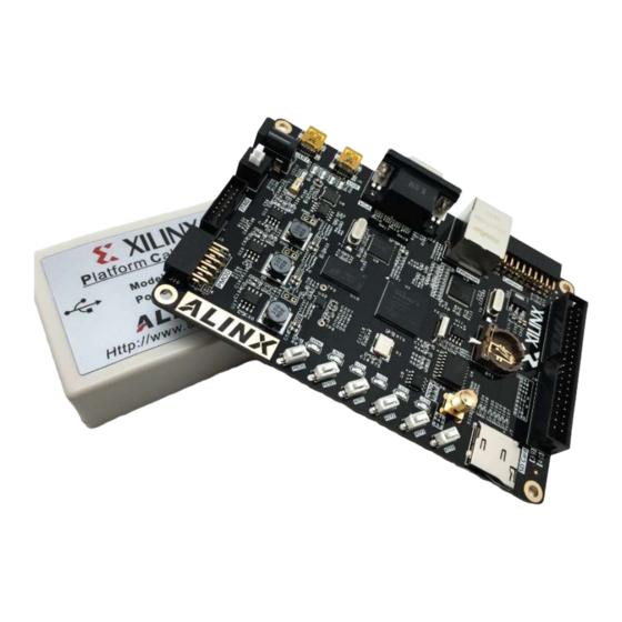
- Page 1 Spartan-6 FPGA Development Board AX516 User Manual...
- Page 2 Spartan-6 FPGA Development Board AX516 User Manual Version Record Version Date Release By Description Rev 1.0 2019-04-28 Rachel Zhou First Release 2 / 42 Contact Email: rachel.zhou@alinx.com.cn...
-
Page 3: Table Of Contents
Part 15: Expansion Header ..............34 Part 16: LED ..................... 36 Part 17: Buttons ..................37 Part 18: Camera Module Interface ............39 Part 19: PMOD interface (AX516 Reserved) ..........40 Part 20: SMA Interface ................42 3 / 42 Contact Email: rachel.zhou@alinx.com.cn... -
Page 4: Part 1: Fpga Development Board Introduction
Spartan-6 FPGA Development Board AX516 User Manual The AX516 FPGA development board uses the XILINX SPARTAN6 family chips, model XC6SLX16-2CSG324. As a core processor, FPGA has rich hardware resources and peripheral interfaces. In the design, adhere to the "exquisite, practical, simple" design concept, it is very suitable for software radio,... - Page 5 Table 1-2: The Main Resources and Feature of Xilinx Spartan6 XC6SLX9 The layout of the board that indicates the location of the connector and key components, provide a quickly overview of AX516 board (see Figure 1-2) 5 / 42 Contact Email: rachel.zhou@alinx.com.cn...
- Page 6 按键2 按键3 按键4 SD卡座 Figure 2-1: The Layout of the AX516 board Through this diagram, we can see the functions that the development platform can achieve. +5V power input, maximum 2A current protection A large 128Mbyte high-speed DD3 SDRAM can be used as a buffer for data or as a memory for Microblaze ...
-
Page 7: Part 2: Structure Diagram
On-board 50M active crystal oscillator provides stable clock source for FPGA development board 1-Way 40-pin ALINX expansion port (0.1”inch), 34 IO ports, one 5V power supply, two 3.3V power supplies, three GND. Two expansion modules can be connected at the same time, such as expansion modules such as 4.3-inch TFT module and AD/DA module. -
Page 8: Part 3: Power
Spartan-6 FPGA Development Board AX516 User Manual Figure 2-1: Structure Diagram Part 3: Power The FPGA development board power supply input voltage is DC5V. The power supply design diagram on the development board is as Figure 3-1: 5V 电源 输入... - Page 9 Spartan-6 FPGA Development Board AX516 User Manual The development board is powered by +5V, and is converted into +3.3V, +1.2V, +1.5V three-way power supply through three-way DC/DC power supply chip MP1482. It generates +2.5V power supply through one LDO LT1117, and VTT and VREF voltages (1.5V) required for DDR3 is generated by TPS51200 of...
-
Page 10: Part 4: Fpga Chip
Spartan-6 FPGA Development Board AX516 User Manual When designing the PCB, we used a 6-layer PCB and reserved a separate Power layer and GND layer, which ensures the FPGA development board has very good stability. On the PCB we have reserved test points for each power supply so that the user can confirm the voltage on the board. -
Page 11: Part 4.1: Jtag Interface
Spartan-6 FPGA Development Board AX516 User Manual Figure 4-1: FPGA Chipset Part 4.1: JTAG Interface First, let's talk about the FPGA configuration and debug interface: the JTAG interface. The function of the JTAG interface is to download the compiled program (.bit) to the FPGA or download the FLASH configuration program (.mcs) to the SPI FLASH. -
Page 12: Part 4.2: Fpga Power Supply
Spartan-6 FPGA Development Board AX516 User Manual Figure 4-2: Hardware Design of JTAG Connector JTAG connector is 14pin connectors, the pin pitch is 2.0mm. Figure 4-3: Onboard JTAG Connector Part 4.2: FPGA Power Supply Next, let's talk about the power supply pin part of the FPGA, including the power supply pin of each bank, the core voltage pin and the auxiliary voltage pin. - Page 13 Spartan-6 FPGA Development Board AX516 User Manual VCCINT is the FPGA core power supply pin, connected to 1.2V; VCCAUX is the FPGA auxiliary power supply pin, can be connected to 3.3V or 2.5V, here connected to 3.3V; VCCINT and VCCAUX connection as shown in Figure 3-4 Figure 4-4: FPGA Power Supply VCCIO is the supply voltage of each BANK of the FPGA.
-
Page 14: Part 5: 50Mhz Clock
Spartan-6 FPGA Development Board AX516 User Manual Figure 4-5: FPGA power supply VCCIO pin Part 5: 50Mhz Clock Figure 5-1 is the clock circuit of the FPGA development board, an 50Mhz crystal oscillator provides the clock source for the whole board. The output of the crystal oscillator is connected to the FPGA global clock (GCLK Pin V10). -
Page 15: Part 6: Qspi Flash
Table 5-1: Clock Pin Assignment Part 6: QSPI Flash The AX516 FPGA development board is equipped with one 128MBit QSPI FLASH, and the model is W25Q128 which uses the 3.3V CMOS voltage standard. Due to the non-volatile nature of QSPI FLASH, it can be used as a boot device for the system to store the boot image of the system. -
Page 16: Part 7: Ddr3 Dram
QSPI_MISO2 QSPI_MISO3 Part 7: DDR3 DRAM The AX516 FPGA development board is equipped with one high speed DDR3 DRAM, Model:MT41J64M16LA-187E, Capacity 128MByte (64M*16bit); 16bit bus. The FPGA and DDR3 DRAM on the development board are connected to the IO of BANK3. The Spartan6 FPGA has a hard DDR3 controller MCB inside. - Page 17 Spartan-6 FPGA Development Board AX516 User Manual DDR3. Figure 7-1 detailed the DDR3 DRAM hardware connection Figure 7-1: DDR3 DRAM Hardware Connection Figure 7-2: DDR3 DRAM on the FPGA Board 17 / 42 Contact Email: rachel.zhou@alinx.com.cn...
- Page 18 Spartan-6 FPGA Development Board AX516 User Manual DDR3 DRAM Pin Assignment: Pin Name FPGA Pin DDR3_LDQS_P DDR3_LDQS_N DDR3_UDQS_P DDR3_UDQS_N DDR3_DQ[0] DDR3_DQ [1] DDR3_DQ [2] DDR3_DQ [3] DDR3_DQ [4] DDR3_DQ [5] DDR3_DQ [6] DDR3_DQ [7] DDR3_DQ [8] DDR3_DQ [9] DDR3_DQ [10]...
-
Page 19: Part 8: Eeprom 24Lc04
Spartan-6 FPGA Development Board AX516 User Manual DDR3_A [9] DDR3_A [10] DDR3_A [11] DDR3_A [12] DDR3_A [13] DDR3_BA [0] DDR3_BA [1] DDR3_BA [2] DDR3_RAS_N DDR3_CAS_N DDR3_WE_N DDR3_ODT DDR3_RESET_N DDR3_CLK_P DDR3_CLK_N DDR3_CKE Part 8: EEPROM 24LC04 The development board contains an EEPROM, model 24LC04, and its capacity is 4Kbit (2*256*8bit). -
Page 20: Part 9: Real Time Clock Ds1302
Spartan-6 FPGA Development Board AX516 User Manual Figure 8-1: EEPROM Design Figure 8-2 shows the EEPROM on AX516 board: Figure 8-2: EEPROM on AX516 board Table 8-1 detailed the EEPROM PIN assignment Net Name FPGA PIN Table 8-1: EEPROM PIN Assignment... - Page 21 Spartan-6 FPGA Development Board AX516 User Manual passive clock to provide an accurate clock source to the clock chip, so that the RTC can accurately provide clock information to the product. At the same time, in order to power off the product, the real-time clock can still run normally.
-
Page 22: Part 10: Gigabit Ethernet Interface
Spartan-6 FPGA Development Board AX516 User Manual Figure 9-2: DS1302 Circuit Onboard Table 9-1 detailed the DS1302 Pin Assignment: Net Name FPGA PIN RTC_I2C_SCL RTC_RESET RTC_I2C_SDA Table 9-1: The DS1302 Pin Assignment Part 10: Gigabit Ethernet Interface The FPGA development board provides network communication services through the Realtek RTL8211EG Ethernet PHY chip. - Page 23 Spartan-6 FPGA Development Board AX516 User Manual Configuration Pin Instructions Configuration value PHYAD[2:0] MDIO/MDC Mode PHY Address PHY Address 011 3.3V, 2.5V, 1.5/1.8V voltage SELRGV 3.3V selection AN[1:0] Auto-negotiation configuration (10/100/1000M) adaptive RX Delay Delay RX clock 2ns delay TX Delay...
- Page 24 Spartan-6 FPGA Development Board AX516 User Manual Figure 10-2: Gigabit Ethernet interface on the FPGA board Ethernet pin assignments are as follows: Signal Name FPGA Pin Description Ethernet GMII transmit clock E_GCLK Ethernet Transmit Data bit0 E_TXD0 Ethernet Transmit Data bit1...
-
Page 25: Part 11: Usb To Serial Port
Spartan-6 FPGA Development Board AX516 User Manual Ethernet Receive Data Bit1 E_RXD1 Ethernet Receive Data Bit2 E_RXD2 Ethernet Receive Data Bit3 E_RXD3 Ethernet Receive Data Bit4 E_RXD4 Ethernet Receive Data Bit5 E_RXD5 Ethernet Receive Data Bit6 E_RXD6 Ethernet Receive Data Bit7... - Page 26 Spartan-6 FPGA Development Board AX516 User Manual Figure 11-2: USB to Serial Port Circuit Onboard At the same time, three LED indicators (LED7, LED8, LED9) are set for the serial port signal. When the UART port (J2) is connected to the USB port of the PC, LED9 is on;...
-
Page 27: Part 12: Vga Port
Spartan-6 FPGA Development Board AX516 User Manual Figure 11-4: USB to serial signal indicator on FPGA Board Serial port pin assignment: Pin Name FPGA Pin UART_RXD UART_TXD UART_CTS UART_RTS Table11-1: The PIN Assignment of Serial Port Part 12: VGA Port VGA interface, I believe many friends will not be unfamiliar, because this interface is the most important interface on the computer monitor. - Page 28 Spartan-6 FPGA Development Board AX516 User Manual The three primary color source terminals and terminal matching resistors are both 75 ohms, detailed as Figure 12-1 Figure 12-1: VGA video signal transmission diagram HSYNC and VSYNC are line data synchronization and frame data synchronization, respectively, which are TTL levels.
-
Page 29: Part 13: Usb 2.0
Spartan-6 FPGA Development Board AX516 User Manual Figure 12-3: VGA Interface on board VGA Interface Pin Assignment Signal Name FPGA PIN Description BLUE[0] VGA_B[0] BLUE[1] VGA_B[1] BLUE[2] VGA_B[2] BLUE[3] VGA_B[3] BLUE[4] VGA_B[4] GREEN[0] VGA_G[0] GREEN[1] VGA_G[1] GREEN[2] VGA_G[2] GREEN[3] VGA_G[3]... - Page 30 Spartan-6 FPGA Development Board AX516 User Manual high-speed data communication between PC and FPGA. CY7C68013A controller fully complies with the universal serial bus protocol version 2.0 specifications, supports full speed (12Mbit/s) and low speed (480Mbit/s) mode. The user can perform USB2.0 data communication by connecting the USB port of the PC with the USB cable and the MINI type USB port (J6) of the development board.
- Page 31 Spartan-6 FPGA Development Board AX516 User Manual Figure 13-2: USB2.0 part circuit on board USB 2.0 Pin Assignment Pin Name FPGA Pin Description 12-, 24- or 48 MHz clock output USB_CLKOUT Synchronous communication clock signal USB_IFCLK Status output signal USB_FLAGA...
-
Page 32: Part 14: Sd Card Slot
Spartan-6 FPGA Development Board AX516 User Manual USB data Bit4 USB_FD[4] USB data Bit5 USB_FD[5] USB data Bit6 USB_FD[6] USB data Bit7 USB_FD[7] USB data Bit8 USB_FD[8] USB data Bit9 USB_FD[9] USB data Bit10 USB_FD[10] USB data Bit11 USB_FD[11] USB data Bit12... - Page 33 Spartan-6 FPGA Development Board AX516 User Manual Figure 14-1: SD Socket Design Figure 14-2: SD Card Slot On board SD Card Slot Pin Assignment: SD Mode FPGA Pin Pin Name SD_CLK SD_CMD SD_CD_N SD_DAT0 SD_DAT1 SD_DAT2 SD_DAT3 Table 14-1: The Pin Assignment of SD Card Slot 33 / 42 Contact Email: rachel.zhou@alinx.com.cn...
-
Page 34: Part 15: Expansion Header
Spartan-6 FPGA Development Board AX516 User Manual Part 15: Expansion Header The development board reserves 1 expansion ports, and the expansion port has 40 signals, of which 5V power supply 1 way, 3.3V power supply 2 way, ground 3 way, IO port 34 way. These IO ports are independent IO ports and are not multiplexed with other devices. - Page 35 Spartan-6 FPGA Development Board AX516 User Manual Figure 15-2: J3 Expansion Headers on Board Figure 15-3: Expansion port connected the expansion module J3 Expansion Port Pin Assignment Pin Number FPGA Pin Pin Number FPGA Pin VCC5V 35 / 42 Contact Email: rachel.zhou@alinx.com.cn...
-
Page 36: Part 16: Led
Spartan-6 FPGA Development Board AX516 User Manual VCC3V3 VCC3V3 Part 16: LED The FPGA development board contains six LEDs, including four user LEDs, two FPGA configuration LEDs. The schematic of the four user LEDs is shown in Figure 16-1. When the pin output of the FPGA is logic 0, the LED will be lit. -
Page 37: Part 17: Buttons
Spartan-6 FPGA Development Board AX516 User Manual Figure 16-2: Configuration Indicator LED schematic Figure 16-3: LEDs on Board LEDs Pin Assignment Pin Name FPGA Pin LED0 LED1 LED2 LED3 Table 16-1: The Pin Assignment of LEDs Part 17: Buttons The board has six buttons, it includes four user buttons (KEY1~KEY4) and... - Page 38 Spartan-6 FPGA Development Board AX516 User Manual Figure 17-1: 4 user button schematics The schematic diagram of the two function buttons is shown in Figure 16.2, where the Reset button is connected to the FPGA's normal IO for FPGA program reset, and the PROG button is connected to the FPGA's dedicated PROGRAM_B pin for FPGA program reconfiguration.
-
Page 39: Part 18: Camera Module Interface
Spartan-6 FPGA Development Board AX516 User Manual Part 18: Camera Module Interface The AX516 FPGA development board includes an 18-pin CMOS camera interface that can be connected to the OV7670 camera module and the OV5640 camera module to enable video capture. After acquisition, the display can be connected via a TFT LCD module or a VGA interface. -
Page 40: Part 19: Pmod Interface (Ax516 Reserved)
The development board reserves a 12-pin 2.54mm pitch PMOD interface (J10) for connecting external modules or circuits. The PMOD interface is reserved for the AX516 development board (Spartan6 XC6SLX16 chip). However, for the AX545 development board, the pins of this PMOD interface are NC on the XC6SLX45 chip. - Page 41 Spartan-6 FPGA Development Board AX516 User Manual is shown in Figure 19-1 Figure 19-1: PMOD Interface Schematic Figure 19-2: PMOD on FPGA Board PMOD interface pin assignment PMOD Pin FPGA Pin Description AX545 is not available AX545 is not available...
-
Page 42: Part 20: Sma Interface
Spartan-6 FPGA Development Board AX516 User Manual AX545 is not available VCC3V3 Part 20: SMA Interface The SMA interface (J27) on the development board is connected to the global clock input and output pins of the FPGA, and the user can freely use it according to his own needs.
Need help?
Do you have a question about the AX516 and is the answer not in the manual?
Questions and answers