Table of Contents
Advertisement
Quick Links
Advertisement
Table of Contents

Subscribe to Our Youtube Channel
Related Manuals for Alinx AXKU041


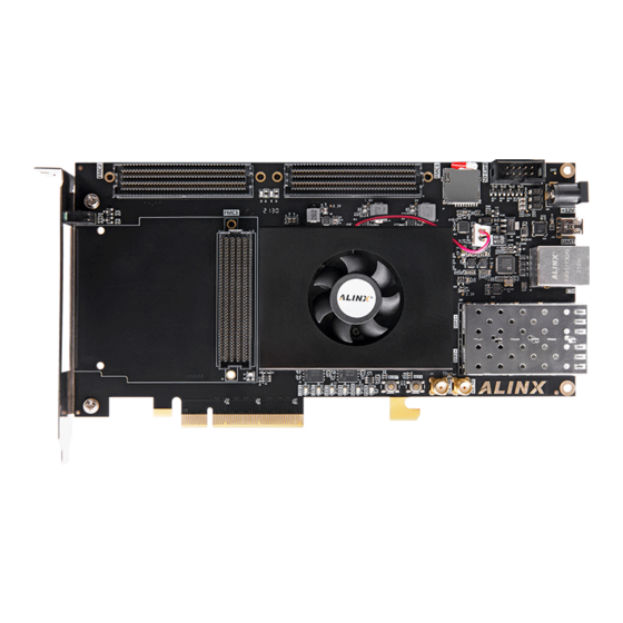
Summary of Contents for Alinx AXKU041
- Page 1 KINTEX UltraScale development Board User Manual AXKU041...
- Page 2 AXKU041UserManual Version Record Version Date REV1.0 2020-2-1 2 / 56...
-
Page 3: Table Of Contents
Part 11 FMC connector Part 11 SD Card Slot Part 12 SMA、SATA Interface Part 13 temperature sensor Part 14 JTAG Part 15 LED Part 16 Buttons Part 17 Power Supply Part 18 FAN Part 19 Structural dimension drawing http://www.alinx.com 3 / 56... -
Page 4: Part 1 Fpga Development Board Introduction
To give you a quick overview of this development platform, we have written this user manual. The AXKU041 development board is mounted with four 1GB high-speed DDR4 SDRAM chips, and the FPGA chip configuration uses two 256Mb QSPI NOR FLASH chips. - Page 5 (4GB). Can be used as FPGA data storage, image analysis cache, data processing. QSPI FLASH Two 256Mbit QSPI NOR FLASH memory chips, which can be used to store FPGA chip configuration files and user data; 2 SFP+Fiber Interface http://www.alinx.com 5 / 56...
- Page 6 AXKU041UserManual The two-channel high-speed transceiver of THE GTH transceiver of FPGA is connected to the transmitting and receiving of two optical modules to realize the two-channel high-speed optical communication interface. Each channel of optical fiber data communication receives and sends up to 16.3Gb/s ...
- Page 7 LED Light 6 leds, 1 power indicator; 1 DONE configuration indicator; 4 user indicators and a pair of panel indicators. Button 2 user buttons, 1 reset button, and 1 normal IO connected to FPGA http://www.alinx.com 7 / 56...
-
Page 8: Part 2 Fpga Chip
AXKU041UserManual Part 2 FPGA Chip The development board uses Xilinx's KINTEX UltraSacale chip, model XCKU040- 2FFVA1156I. The speed grade is 2 and the temperature grade is industrial grade. This model is FFVA1156 package, 1156 pins, pin spacing 1.0mm. Figure 2-1 shows the chip naming rules of Xilinx KINTEX UltraSacale:... -
Page 9: Fpga Power Supply System
GTH sending and receiving, connected to 1.2V. V Calibrate voltage for MGTAVTTRCAL transceiver resistor, connected to 1.2V;V Supply voltage for XADC, 1.8V。 CCADC Figure 2-2 shows the sequence for powering on the XCKU040 FPGA system Figure 2-2 http://www.alinx.com 9 / 56... -
Page 10: Part4 Ddr4 Dram
AXKU041UserManual Part4 DDR4 DRAM The AXKU040 development board is equipped with four Micron 1GB DDR4 chips, model mt40A512M16LY-062EIT. Four DDR4 SDRAM chips form a 64-bit bus width. Because the four DDR4 chips are connected to the FPGA, DDR4 SDRAM has a maximum operating clock of 1200Mhz, and the four DDR4 storage systems are directly connected to the BANK44, BANK45, and BANK46 interfaces of the FPGA. - Page 11 PL_DDR4_DQ4 IO_L3P_T0L_N4_AD15P_44 AD20 PL_DDR4_DQ5 IO_L6N_T0U_N11_AD6N_44 AG22 PL_DDR4_DQ6 IO_L6P_T0U_N10_AD6P_44 AF22 PL_DDR4_DQ7 IO_L5N_T0U_N9_AD14N_44 AE23 PL_DDR4_DQ8 IO_L8N_T1L_N3_AD5N_44 AF24 PL_DDR4_DQ9 IO_L11P_T1U_N8_GC_44 AJ23 PL_DDR4_DQ10 IO_L8P_T1L_N2_AD5P_44 AF23 PL_DDR4_DQ11 IO_L12N_T1U_N11_GC_44 AH23 PL_DDR4_DQ12 IO_L9N_T1L_N5_AD12N_44 AG25 PL_DDR4_DQ13 IO_L11N_T1U_N9_GC_44 AJ24 PL_DDR4_DQ14 IO_L9P_T1L_N4_AD12P_44 AG24 PL_DDR4_DQ15 IO_L12P_T1U_N10_GC_44 AH22 http://www.alinx.com 11 / 56...
- Page 12 AXKU041UserManual PL_DDR4_DQ16 IO_L14P_T2L_N2_GC_44 AK22 PL_DDR4_DQ17 IO_L17P_T2U_N8_AD10P_44 AL22 PL_DDR4_DQ18 IO_L15N_T2L_N5_AD11N_44 AM20 PL_DDR4_DQ19 IO_L17N_T2U_N9_AD10N_44 AL23 PL_DDR4_DQ20 IO_L14N_T2L_N3_GC_44 AK23 PL_DDR4_DQ21 IO_L18N_T2U_N11_AD2N_44 AL25 PL_DDR4_DQ22 IO_L15P_T2L_N4_AD11P_44 AL20 PL_DDR4_DQ23 IO_L18P_T2U_N10_AD2P_44 AL24 PL_DDR4_DQ24 IO_L20P_T3L_N2_AD1P_44 AM22 PL_DDR4_DQ25 IO_L23P_T3U_N8_44 AP24 PL_DDR4_DQ26 IO_L20N_T3L_N3_AD1N_44 AN22 PL_DDR4_DQ27 IO_L21N_T3L_N5_AD8N_44 AN24 PL_DDR4_DQ28 IO_L24P_T3U_N10_44 AN23 PL_DDR4_DQ29 IO_L23N_T3U_N9_44 AP25...
- Page 13 PL_DDR4_DQS1_P IO_L10P_T1U_N6_QBC_AD4P_44 AH24 PL_DDR4_DQS1_N IO_L10N_T1U_N7_QBC_AD4N_44 AJ25 PL_DDR4_DQS2_P IO_L16P_T2U_N6_QBC_AD3P_44 AJ20 PL_DDR4_DQS2_N IO_L16N_T2U_N7_QBC_AD3N_44 AK20 PL_DDR4_DQS3_P IO_L22P_T3U_N6_DBC_AD0P_44 AP20 PL_DDR4_DQS3_N IO_L22N_T3U_N7_DBC_AD0N_44 AP21 PL_DDR4_DQS4_P IO_L4P_T0U_N6_DBC_AD7P_46 AL27 PL_DDR4_DQS4_N IO_L4N_T0U_N7_DBC_AD7N_46 AL28 PL_DDR4_DQS5_P IO_L10P_T1U_N6_QBC_AD4P_46 AN29 PL_DDR4_DQS5_N IO_L10N_T1U_N7_QBC_AD4N_46 AP30 PL_DDR4_DQS6_P IO_L16P_T2U_N6_QBC_AD3P_46 AH33 PL_DDR4_DQS6_N IO_L16N_T2U_N7_QBC_AD3N_46 AJ33 http://www.alinx.com 13 / 56...
- Page 14 AXKU041UserManual PL_DDR4_DQS7_P IO_L22P_T3U_N6_DBC_AD0P_46 AN34 PL_DDR4_DQS7_N IO_L22N_T3U_N7_DBC_AD0N_46 AP34 PL_DDR4_A0 IO_L18N_T2U_N11_AD2N_45 AG14 PL_DDR4_A1 IO_L23N_T3U_N9_45 AF17 PL_DDR4_A2 IO_L20P_T3L_N2_AD1P_45 AF15 PL_DDR4_A3 IO_L16N_T2U_N7_QBC_AD3N_45 AJ14 PL_DDR4_A4 IO_L19N_T3L_N1_DBC_AD9N_45 AD18 PL_DDR4_A5 IO_L15P_T2L_N4_AD11P_45 AG17 PL_DDR4_A6 IO_L23P_T3U_N8_45 AE17 PL_DDR4_A7 IO_L11N_T1U_N9_GC_45 AK18 PL_DDR4_A8 IO_L24P_T3U_N10_45 AD16 PL_DDR4_A9 IO_L13P_T2L_N0_GC_QBC_45 AH18 PL_DDR4_A10 IO_L19P_T3L_N0_DBC_AD9P_45 AD19 PL_DDR4_A11 IO_L24N_T3U_N11_45 AD15...
-
Page 15: Prat 5 Qspi Flash
CCLK0 of BANK0. Figure 4-2 shows the connection diagram of QSPI FLASH and FPGA chip Figure 4-2 QSPI Flash Signal Name FPGA Pin Name FPGA Pin Number QSPI_CCLK CCLK_0 QSPI0_CS_B RDWR_FCS_B_0 http://www.alinx.com 15 / 56... - Page 16 AXKU041UserManual QSPI0_IO0 D00_MOSI_0 QSPI0_IO1 D01_DIN_0 QSPI0_IO2 D02_0 QSPI0_IO3 D03_0 Signal Name FPGA Pin Name FPGA Pin Number QSPI1_CS_B IO_L2N_T0L_N3_FWE_FCS2_B_65 QSPI1_IO0 IO_L22P_T3U_N6_DBC_AD0P_D04_65 QSPI1_IO1 IO_L22N_T3U_N7_DBC_AD0N_D05_65 QSPI1_IO2 IO_L21P_T3L_N4_AD8P_D06_65 QSPI1_IO3 IO_L21N_T3L_N5_AD8N_D07_65 16 / 56...
-
Page 17: Part6 Clock Configuration
GTH. The crystal oscillator differential output is connected to FPGA BANK226, this clock is used for the clock required for 2 channels of optical fiber. Figure 5-2 shows the working principle of the clock http://www.alinx.com 17 / 56... - Page 18 AXKU041UserManual source Figure 5-2 Clock pin assignments: Signal Name FPGA Pin SFP_CLK0_P SFP_CLK0_N 156.25Mhz Differential clock source A differential 156.25mhz clock source is provided on the board to provide the clock for the transceiver GTH. Crystal oscillator differential output connected to FPGA BANK228.
- Page 19 Clock pin assignments: Signal Name FPGA Pin HDMI_DRU_CLOCK_P HDMI_DRU_CLOCK_N http://www.alinx.com 19 / 56...
-
Page 20: Usb To Serial Port
AXKU041UserManual Part 7 USB to Serial Port AXKU040 development board is equipped with a Uart to USB interface for development board serial communication and debugging. The conversion chip is usB-UAR chip of Silicon Labs CP2102GM, and a level conversion chip is used to connect CP2102 serial port chip and FPGA to adapt to different FPGA BANK voltages. -
Page 21: Sfp+Fiber Interface
The 1st fiber interface FPGA pin assignment is as follows: Signal Name FPGA pin Description SFP1_TX_P SFP1 Data Transfer Positive SFP1_TX_N SFP1 Data Transfer Negative SFP1_RX_P SFP1 Data Receiver Positive SFP1_RX_N SFP1 Data Receiver Negative SFP1_TX_DIS AC22 SFP1 Optical Transfer Disable, http://www.alinx.com 21 / 56... - Page 22 AXKU041UserManual active high SFP1_LOSS AF28 SFP1 Optical LOSS,High level means no light signal is received The 2 fiber interface FPGA pin assignment is as follows: Signal Name FPGA PIN Description SFP2_TX_P SFP2 Data Transfer Positive SFP2_TX_N SFP2 Data Transfer Negative SFP2_RX_P SFP2 Data Receiver Positive SFP2_RX_N...
-
Page 23: Part 9 Ethernet Interface
Part 9 Ethernet interface AXKU041 has one gigabit Ethernet interface, and the GPHY chip uses Micrel's KSZ9031RNX Ethernet chip provide network communication services. KSZ9031RNX chip supports 10/100/1000 Mbps network transmission rate, through RGMII interface with the MAC layer of the system for data communication. - Page 24 AXKU041UserManual Figure 8-1 Ethernet FPGA pins are assigned as follows: Signal Name PIN Name FPGA PHY_GTXC IO_L22P_T3U_N6_DBC_AD0P_64 PHY_TXD0 IO_L22N_T3U_N7_DBC_AD0N_64 PHY_TXD1 IO_L24N_T3U_N11_64 PHY_TXD2 IO_L20N_T3L_N3_AD1N_64 PHY_TXD3 IO_L21N_T3L_N5_AD8N_64 PHY_TXEN IO_L20P_T3L_N2_AD1P_64 PHY_RXC IO_L14P_T2L_N2_GC_64 PHY_RXD0 IO_L23N_T3U_N9_64 PHY_RXD1 IO_L23P_T3U_N8_64 PHY_RXD2 IO_L24P_T3U_N10_64 PHY_RXD3 IO_L21P_T3L_N4_AD8P_64 AK10 PHY_RXDV IO_L14N_T2L_N3_GC_64 PHY_MDC IO_T1U_N12_64 AJ11...
-
Page 25: Part 10 Pcie X8 Interface
Part 10 PCIE X8 Interface AXKU041 is equipped with a pci 3.0x8 interface. Eight pairs of transceivers are connected to the gold finger of PCIEx8 to achieve data communication between PCIEx8, pci ex4, PCIex2 and PCIex1. The transceiver signal of PCIe interface is directly connected with GTH transceiver of FPGA BANK224 and BANK225. - Page 26 AXKU041UserManual PCIE_RX1_P MGTHRXP2_225 PCIE_RX2_N MGTHRXN1_225 PCIE_RX2_P MGTHRXP1_225 PCIE_RX3_N MGTHRXN0_225 PCIE_RX3_P MGTHRXP0_225 PCIE_RX4_N MGTHRXN3_224 PCIE_RX4_P MGTHRXP3_224 PCIE_RX5_N MGTHRXN2_224 PCIE_RX5_P MGTHRXP2_224 PCIE_RX6_N MGTHRXN1_224 PCIE_RX6_P MGTHRXP1_224 PCIE_RX7_N MGTHRXN0_224 PCIE_RX7_P MGTHRXP0_224 PCIE_TX0_N MGTHTXN3_225 PCIE_TX0_P MGTHTXP3_225 PCIE_TX1_N MGTHTXN2_225 PCIE_TX1_P MGTHTXP2_225 PCIE_TX2_N MGTHTXN1_225 PCIE_TX2_P MGTHTXP1_225 PCIE_TX3_N MGTHTXN0_225 PCIE_TX3_P MGTHTXP0_225...
-
Page 27: Part 11 Fmc Connector
Part 11 FMC connector AXKU041 development board has 2-channel standard FMC LPC expansion port and 1-channel standard FMC HPC expansion port, which can be connected to XILINX or our various FMC modules (HDMI input-output module, bineye camera module, high-speed AD module). - Page 28 AXKU041UserManual Figure 10-2 Figure 9-3 shows the schematic diagram of the HPC connector of FPGA and FMC3: Figure 10-3 HPC FMC3 28 / 56...
- Page 29 IO_L4P_T0U_N6_DBC_AD7P_47 AC26 data P FMC reference 3rd channel FMC1_LPC_LA03_N IO_L4N_T0U_N7_DBC_AD7N_47 AC27 data N FMC reference 4 channel FMC1_LPC_LA04_P IO_L6P_T0U_N10_AD6P_47 AB25 data P FMC reference 4 channel FMC1_LPC_LA04_N IO_L6N_T0U_N11_AD6N_47 AB26 data N FMC reference 5 FMC1_LPC_LA05_P IO_L21P_T3L_N4_AD8P_47 http://www.alinx.com 29 / 56...
- Page 30 AXKU041UserManual channeldata P FMC reference 5 channel FMC1_LPC_LA05_N IO_L21N_T3L_N5_AD8N_47 data N FMC reference 6 channel FMC1_LPC_LA06_P IO_L19P_T3L_N0_DBC_AD9P_47 data P FMC reference 6 channel FMC1_LPC_LA06_N IO_L19N_T3L_N1_DBC_AD9N_47 data N FMC reference 7 channel FMC1_LPC_LA07_P IO_L9P_T1L_N4_AD12P_47 AA20 data P FMC reference 7 channel FMC1_LPC_LA07_N IO_L9N_T1L_N5_AD12N_47 AB20...
- Page 31 AG34 data N FMC reference 20 channel FMC1_LPC_LA20_P IO_L10P_T1U_N6_QBC_AD4P_48 AE33 data P FMC reference 20 channel FMC1_LPC_LA20_N IO_L10N_T1U_N7_QBC_AD4N_48 AF34 data N FMC reference 21st FMC1_LPC_LA21_P IO_L9P_T1L_N4_AD12P_48 AE32 channel data P FMC reference 21st FMC1_LPC_LA21_N IO_L9N_T1L_N5_AD12N_48 AF32 http://www.alinx.com 31 / 56...
- Page 32 AXKU041UserManual channel data N FMC reference 22 channel FMC1_LPC_LA22_P IO_L15P_T2L_N4_AD11P_48 AC34 data P FMC reference 22 channel FMC1_LPC_LA22_N IO_L15N_T2L_N5_AD11N_48 AD34 data N FMC reference 23 FMC1_LPC_LA23_P IO_L17P_T2U_N8_AD10P_48 AA34 channel data P FMC reference 23 channel FMC1_LPC_LA23_N IO_L17N_T2U_N9_AD10N_48 AB34 data N FMC reference 24 channel FMC1_LPC_LA24_P...
- Page 33 AH11 reference clock N FMC reference 2 FMC2_LPC_CLK1_P IO_L14P_T2L_N2_GC_A04_D20_65 reference clock P FMC reference 2 FMC2_LPC_CLK1_N IO_L14N_T2L_N3_GC_A05_D21_65 reference clock N FMC reference 0 FMC2_LPC_LA00_CC_P IO_L11P_T1U_N8_GC_64 AG12 channel data clock P FMC reference 0 FMC2_LPC_LA00_CC_N IO_L11N_T1U_N9_GC_64 AH12 http://www.alinx.com 33 / 56...
- Page 34 AXKU041UserManual channel data (clock) N FMC reference 1 channel FMC2_LPC_LA01_CC_P IO_L13P_T2L_N0_GC_QBC_64 AF10 data (clock) P FMC reference 1 channel FMC2_LPC_LA01_CC_N IO_L13N_T2L_N1_GC_QBC_64 AG10 data (clock) N FMC reference 2 channel FMC2_LPC_LA02_P IO_L2P_T0L_N2_64 AN13 data P FMC reference 2 FMC2_LPC_LA02_N IO_L2N_T0L_N3_64 AP13 channel data N FMC reference 3 FMC2_LPC_LA03_P...
- Page 35 AD11 channel data P FMC reference 15 FMC2_LPC_LA15_N IO_L10N_T1U_N7_QBC_AD4N_64 AE11 channel data N FMC reference 16 FMC2_LPC_LA16_P IO_L7P_T1L_N0_QBC_AD13P_64 AE13 channel data P FMC reference 16 FMC2_LPC_LA16_N IO_L7N_T1L_N1_QBC_AD13N_64 AF13 channel data N FMC reference 17 FMC2_LPC_LA17_CC_P IO_L12P_T1U_N10_GC_A08_D24_6 http://www.alinx.com 35 / 56...
- Page 36 AXKU041UserManual channel data P FMC reference 17 IO_L12N_T1U_N11_GC_A09_D25_6 FMC2_LPC_LA17_CC_N channel data N FMC reference 18 FMC2_LPC_LA18_CC_P IO_L11P_T1U_N8_GC_A10_D26_65 channel data P FMC reference 18 FMC2_LPC_LA18_CC_N IO_L11N_T1U_N9_GC_A11_D27_65 channel data N FMC reference 19 IO_L16P_T2U_N6_QBC_AD3P_A00_ FMC2_LPC_LA19_P D16_65 channel data P FMC reference 19 IO_L16N_T2U_N7_QBC_AD3N_A01 FMC2_LPC_LA19_N channel data N...
- Page 37 FMC reference 31 IO_L19N_T3L_N1_DBC_AD9N_D11 FMC2_LPC_LA31_N channel data N FMC reference 32 FMC2_LPC_LA32_P IO_L6P_T0U_N10_AD6P_A20_65 channel data P FMC reference 32 FMC2_LPC_LA32_N IO_L6N_T0U_N11_AD6N_A21_65 channel data N FMC reference 33 FMC2_LPC_LA33_P IO_L3P_T0L_N4_AD15P_A26_65 channel data P FMC reference 33 FMC2_LPC_LA33_N IO_L3N_T0L_N5_AD15N_A27_65 http://www.alinx.com 37 / 56...
- Page 38 AXKU041UserManual channel data N FMC I2C Bus Clock FMC2_LPC_SCL IO_L23P_T3U_N8_I2C_SCLK_65 FMC I2C Bus Data FMC2_LPC_SDA IO_L23N_T3U_N9_I2C_SDA_65 Transceiver data output FMC2_DP0_C2M_P MGTHTXP2_226 Transceiver data output FMC2_DP0_C2M_N MGTHTXN2_226 Transceiver data input FMC2_DP0_M2C_P MGTHRXP2_226 Transceiver data input FMC2_DP0_M2C_N MGTHRXN2_226 FMC2_GBTCLK0_M2C_P MGTREFCLK1P_226 Transceiver reference clock Transceiver reference clock FMC2_GBTCLK0_M2C_N MGTREFCLK1N_226...
- Page 39 FMC_HPC_LA08_N IO_L6N_T0U_N11_AD6N_67 data N FMC reference 9 channel FMC_HPC_LA09_P IO_L8P_T1L_N2_AD5P_67 data P FMC reference 9 channel FMC_HPC_LA09_N IO_L8N_T1L_N3_AD5N_67 data N FMC reference 10 FMC_HPC_LA10_P IO_L7P_T1L_N0_QBC_AD13P_67 channel data P FMC reference 10 FMC_HPC_LA10_N IO_L7N_T1L_N1_QBC_AD13N_67 channel data N http://www.alinx.com 39 / 56...
- Page 40 AXKU041UserManual FMC reference 11 FMC_HPC_LA11_P IO_L13P_T2L_N0_GC_QBC_67 channel data p FMC reference 11 FMC_HPC_LA11_N IO_L13N_T2L_N1_GC_QBC_67 channel data N FMC reference 12 FMC_HPC_LA12_P IO_L10P_T1U_N6_QBC_AD4P_67 channel data P FMC reference 12 FMC_HPC_LA12_N IO_L10N_T1U_N7_QBC_AD4N_67 channel data N FMC reference 13 FMC_HPC_LA13_P IO_L15P_T2L_N4_AD11P_67 channel data P FMC reference 13 FMC_HPC_LA13_N IO_L15N_T2L_N5_AD11N_67...
- Page 41 IO_L5P_T0U_N8_AD14P_66 channel data P FMC reference 25 FMC_HPC_LA25_N IO_L5N_T0U_N9_AD14N_66 channel data N FMC reference 26 FMC_HPC_LA26_P IO_L2P_T0L_N2_66 channel data P FMC reference 26 FMC_HPC_LA26_N IO_L2N_T0L_N3_66 channel data N FMC reference 27 FMC_HPC_LA27_P IO_L4P_T0U_N6_DBC_AD7P_66 channel data P http://www.alinx.com 41 / 56...
- Page 42 AXKU041UserManual FMC reference 27 FMC_HPC_LA27_N IO_L4N_T0U_N7_DBC_AD7N_66 channel data N FMC reference 28 FMC_HPC_LA28_P IO_L1P_T0L_N0_DBC_66 channel data P FMC reference 28 FMC_HPC_LA28_N IO_L1N_T0L_N1_DBC_66 channel data N FMC reference 29 FMC_HPC_LA29_P IO_L6P_T0U_N10_AD6P_66 channel data P FMC reference 29 FMC_HPC_LA29_N IO_L6N_T0U_N11_AD6N_66 channel data N FMC reference 30 FMC_HPC_LA30_P IO_L9P_T1L_N4_AD12P_66...
- Page 43 FMC HA Route 16 data N FMC_HPC_HA16_N IO_L21N_T3L_N5_AD8N_68 FMC HA Route 17 data P FMC_HPC_HA17_CC_P IO_L11P_T1U_N8_GC_68 FMC HA Route 17 data N FMC_HPC_HA17_CC_N IO_L11N_T1U_N9_GC_68 FMC HA Route 18 data P FMC_HPC_HA18_P IO_L9P_T1L_N4_AD12P_68 FMC HA Route 18 data N FMC_HPC_HA18_N IO_L9N_T1L_N5_AD12N_68 http://www.alinx.com 43 / 56...
- Page 44 AXKU041UserManual FMC HA Route 19 data P FMC_HPC_HA19_P IO_L19P_T3L_N0_DBC_AD9P_68 FMC HA Route 19 data N FMC_HPC_HA19_N IO_L19N_T3L_N1_DBC_AD9N_68 FMC HA Route 20 data P FMC_HPC_HA20_P IO_L15P_T2L_N4_AD11P_68 FMC HA Route 20 data N FMC_HPC_HA20_N IO_L15N_T2L_N5_AD11N_68 FMC HA Route 21 data P FMC_HPC_HA21_P IO_L3P_T0L_N4_AD15P_68 FMC HA Route 21 data N FMC_HPC_HA21_N...
- Page 45 Transceiver data 5 output P FMC_DP5_C2M_P MGTHTXP1_227 Transceiver data 5 output FMC_DP5_C2M_N MGTHTXN1_227 Transceiver data 6 output P FMC_DP6_C2M_P MGTHTXP0_227 Transceiver data 6 output FMC_DP6_C2M_N MGTHTXN0_227 Transceiver data 7 output P FMC_DP7_C2M_P MGTHTXP3_227 Transceiver data 7 output FMC_DP7_C2M_N MGTHTXN3_227 http://www.alinx.com 45 / 56...
-
Page 46: Part 11 Sd Card Slot
AXKU041UserManual Part 11 SD Card Slot The AXKU041 development board includes a Micro SD card interface to provide users with access to SD card memory for storing pictures, music or other user data files. The signal is connected to THE IO signal of BANK48 of FPGA, whose level is 1.8V by default. -
Page 47: Part 12 Sma、Sata Interface
Part 12 SMA、SATA Interface The AXKU041 development board provides two SMA interfaces, differential signals connected to the BANK66 common clock IO port, providing customers with external clock interface or according to the common IO port, interface level is 1.8V. Figure 12-1 shows the interface connection between FPGA and SMA. -
Page 48: Part 13 Temperature Sensor
AXKU041UserManual Part 13 temperature sensor The AXKU040 development board is equipped with a high-precision, low-power, digital temperature sensor chip named ON Semiconductor'S LM75A. The temperature accuracy of LM75A chip is 0.5 degrees. The sensor and FPGA are directly I2C digital interfaces. FPGA reads the temperature near the current development board through the I2C interface. -
Page 49: Part 14 Jtag
Part 14 JTAG A JTAG interface is reserved on the AXKU041 development board for downloading FPGA programs or solidified programs to FLASH. In order to damage FPGA chip caused by charged plug and remove, we added protection diode to JTAG signal to ensure that the signal voltage is within the range accepted by FPGA and avoid FPGA damage. -
Page 50: Part 15 Led
AXKU041UserManual Part 15 LED AXKU041 development board has 6 LED, including 1 power indicator; 1 DONE light, 4 FPGA control lights, and 1 double panel indicator light holder. When the development board is powered on, the power indicator light will light up; When FPGA configures the program, the configuration LED light will light up. - Page 51 Figure 15-2 Signal PIN Name FPGA Name LED1 IO_T1U_N12_PERSTN1_65 LED2 IO_L16N_T2U_N7_QBC_AD3N_47 LED3 IO_L16P_T2U_N6_QBC_AD3P_47 LED4 IO_L18P_T2U_N10_AD2P_47 FPGA_DONE DONE_0 TEST_LED1 IO_L18P_T2U_N10_AD2P_67 TEST_LED2 IO_L18N_T2U_N11_AD2N_67 http://www.alinx.com 51 / 56...
-
Page 52: Part 16 Buttons
AXKU041UserManual Part 16 Buttons The AXKU041 development board has two buttons, one of which is a reset button. 1 user button, user button and reset button are connected to IO of FPGA BANK47. User key low level effective, for customers to achieve some functions of the board;... -
Page 53: Part 17 Power Supply
FPGA chip IO voltage, FMC, optical +3.3V fiber, LED lamp, SD card, level conversion chip HDMI chip, level converter chip +1.8V voltage, power supply voltage 1.2V/1.5A, DDR4, FPGA chip, VOLTAGE on FMC, 1.2V/500mA auxiliary voltage, network port chip http://www.alinx.com 53 / 56... - Page 54 AXKU041UserManual MGTAVCC(+1.0V) FPGA voltage MGTAVTT(+1.2V) FPGA voltage DDRVTT(0.6V) DDR4 Pull-up voltage MGT_1.8V (+1.2V) FPGA GTH boosting voltage 54 / 56...
-
Page 55: Part 18 Fan
BANK48. If the IO level output is high, the MOSFET tube is on, and the fan works. Figure 18-1 shows the fan module design: Figure 18-1 Signal Name PIN Name FPGA PIN Description Fan control pin FAN_PWM IO_T1U_N12_48 AE31 http://www.alinx.com 55 / 56... -
Page 56: Part 19 Structural Dimension Drawing
AXKU041UserManual Part 19 Structural dimension drawing front(Top View) 56 / 56...
Need help?
Do you have a question about the AXKU041 and is the answer not in the manual?
Questions and answers