Table of Contents
Advertisement
Quick Links
E
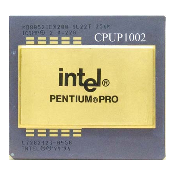
PENTIUM® PRO PROCESSOR AT
150 MHz, 166 MHz, 180 MHz and
n
Available at 150 MHz, 166 MHz,
180 MHz and 200MHz core speeds
n
Binary compatible with applications
running on previous members of the
Intel microprocessor family
n
Optimized for 32-bit applications
running on advanced 32-bit operating
systems
n
Dynamic Execution microarchitecture
n
Single package includes Pentium
processor CPU, cache and system bus
interface
n
Scalable up to four processors and
4 GB memory
®
The Pentium
Pro processor family is Intel's next generation of performance for high-end desktops, workstations
and servers. The family consists of processors at 150 MHz and higher and is easily scalable to up to four
microprocessors in a multiprocessor system. The Pentium Pro processor delivers more performance than
previous generation processors through an innovation called Dynamic Execution. This is the next step beyond
the superscalar architecture implemented in the Pentium processor. This makes possible the advanced 3D
visualization and interactive capabilities required by today's high-end commercial and technical applications and
tomorrow's emerging applications. The Pentium Pro processor also includes advanced data integrity, reliability,
and serviceability features for mission critical applications.
The Pentium Pro processor may contain design defects or errors known as errata which may cause the product
to deviate from published specifications. Current characterized errata are available upon request.
June1997
200 MHz
n
Separate dedicated external system
bus, and dedicated internal full-speed
cache bus
n
8 KB / 8 KB separate data and
instruction, non-blocking, level one
cache
n
Available with integrated 256 KB or
512 KB, non-blocking, level two cache
on package
n
Data integrity and reliability features
®
Pro
include ECC, Fault Analysis/Recovery,
and Functional Redundancy Checking
n
Upgradable to a Future OverDrive
processor
®
Order Number: 242769-005
Advertisement
Table of Contents

Related Manuals for Intel PENTIUM PRO


Summary of Contents for Intel PENTIUM PRO
- Page 1 The Pentium Pro processor also includes advanced data integrity, reliability, and serviceability features for mission critical applications. The Pentium Pro processor may contain design defects or errors known as errata which may cause the product to deviate from published specifications. Current characterized errata are available upon request.
-
Page 2: Table Of Contents
PENTIUM® PRO PROCESSOR AT 150, 166, 180, and 200 MHz CONTENTS PAGE PAGE 1.0. INTRODUCTION ..........4 6.0. THERMAL SPECIFICATIONS......59 1.1. TERMINOLOGY ..........4 6.1. Thermal Parameters........60 1.2. REFERENCES ..........4 6.2. Thermal Analysis..........62 2.0. PENTIUM ® PRO PROCESSOR 7.0. MECHANICAL SPECIFICATIONS ....64 ARCHITECTURE OVERVIEW ...... - Page 3 A.38 NMI (I) ............109 Information in this document is provided in connection with Intel products. No license, express or implied, by estoppel or otherwise, to any intellectual property rights is granted by this document. Except as provided in Intel’s Terms and Conditions of Sale for such products, Intel assumes no liability whatsoever, and Intel disclaims any express or implied warranty, relating to sale and/or use of Intel products including liability or warranties relating to fitness for a particular purpose, merchantability, or infringement of any patent, copyright or other intellectual property right.
-
Page 4: Introduction
D[3:0] = ‘HLHL’ refers to a hex ‘A’, and D#[3:0] = ‘LHLH’ also refers to a hex ‘A’. (H= High The Pentium Pro processor is the next in the logic level, L= Low logic level) Intel386™, Intel486™, and Pentium family of proc- essors. -
Page 5: Full Core Utilization
This approach that, at run time, causes a cache miss. A traditional allows the “execute” phase of the Pentium Pro CPU core must wait for its bus interface unit to read processor to have much more visibility into the this data from main memory and return it before program’s... -
Page 6: The Pentium ® Pro Processor Pipeline
Pro Processor protocol, to system memory. Pipeline In order to get a closer look at how the Pentium Pro processor implements Dynamic Execution, Figure 2 shows a block diagram including cache and memory interfaces. The “Units” shown in Figure 2 represent groups of stages of the Pentium Pro processor pipeline. - Page 7 PENTIUM® PRO PROCESSOR AT 150, 166, 180, and 200 MHz System Bus L2 Cache Bus Interface Unit L1 ICache L1 DCache Fetch Load Store Fetch/ Dispatch Retire Decode /Execute Unit Unit Unit Instruction Pool Figure 2. The Three Core Engines Interface with Memory via Unified Caches •...
- Page 8 MIS in Figure 3). This microcode is just a set of preprogrammed sequences of normal µops. The Pentium Pro processor can schedule at a peak The µops are queued, and sent to the Register Alias rate of 5 µops per clock, one to each resource port, Table (RAT) unit, where the logical IA-based register but a sustained rate of 3 µops per clock is typical.
- Page 9 Figure 5 shows a more detailed view of the Retire But if several are available, it must choose. The Unit. Pentium Pro processor uses a pseudo First In, First Out (FIFO) scheduling algorithm favoring back-to- The retire unit is also checking the status of µops in back µops.
- Page 10 PENTIUM® PRO PROCESSOR AT 150, 166, 180, and 200 MHz To/from DCache RS - Reservation Station MIU - Memory Interface Unit RRF - Retirement Register File From Instruction Pool Figure 5. Inside the Retire Unit MOB - Memory Order Buffer AGU - Address Generation Unit Sys Mem ROB - ReOrder Buffer...
-
Page 11: Architecture Summary
Bus and V recommended when designing a system with a heavily loaded GTL+ bus. See Intel’s world wide web Most of the Pentium Pro processor signals use a page (http:\\www.intel.com) to download the buffer variation of the low voltage Gunning Transceiver models for the Pentium Pro processor in IBIS format. -
Page 12: Power And Ground Pins
L2 cache die may differ from each other. There below their nominal value if not properly controlled. are two groups of power inputs on the Pentium Pro The Pentium Pro processor is also capable of processor package to support the possible voltage... - Page 13 Resistance (ESR) should also be placed near the Decoupling of ten (10) 1µF ceramic capacitors (type Pentium Pro processor in order to handle changes in Y5S or better) and a minimum of five 22µF tantalum average current between the low-power and normal capacitors is recommended for the V S pins.
-
Page 14: Bclk Clock Input Guidelines
PLL1 and PLL2 pins are 3.3 V tolerant and may be driven by existing logic of the Pentium Pro processor. (“Y5R” implies ±15% devices. This is important for both functions of the tolerance over the temperature range -30°C to pins. - Page 15 3.3 V in order to meet the Pentium Pro processor’s 3.3 V tolerant buffer For FRC mode processors, one multiplexer will be specifications. The multiplexer output current should...
-
Page 16: Voltage Identification
0010 1010 There are four Voltage Identification Pins on the 0011 1011 Pentium Pro processor package. These pins can be used to support automatic selection of power supply 0100 1100 voltage. These pins are not signals but are each either an open circuit in the package or a short circuit... -
Page 17: Jtag Connection
Pro processor JTAG logic, it is recommended that SMMEM#, and SPLCK# are all GTL+ signals that are the Pentium Pro processors and any other 3.3 V shared onto another pin. Therefore they do not logic level components within the system be first in appear in this table. -
Page 18: Pwrgood
P is the primary power supply. S is the secondary power supply used by some versions of the second level cache. 5 is unused by Pentium Pro processor and is used by the OverDrive processor for fan/heatsink power. See Section 8. -
Page 19: Thermtrip
PWRGOOD is a 3.3 V tolerant input. It is expected that this signal will be a clean indication that clocks This signal must be supplied to the Pentium Pro and the system 3.3 V, 5 V and V P supplies are processor as it is used to protect internal circuits stable and within their specifications. -
Page 20: Maximum Ratings
When tying any signal to power or ground, a Table 3 contains Pentium Pro processor stress resistor will also allow for fully testing the processor ratings only. Functional operation at the absolute after board assembly. -
Page 21: Dc Specifications
4mΩ of resistance between it and the pins of the processor assuming a regulator set point of ±1%. This voltage is currently not required by the Pentium Pro processor. The voltage is defined for future use. This voltage is required for OverDrive processor support. - Page 22 PENTIUM® PRO PROCESSOR AT 150, 166, 180, and 200 MHz Table 5. Power Specifications 1 Symbol Parameter Unit Notes Thermal Design Power 23.0 29.2 @ 150 MHz, 256K L2 27.5 35.0 @ 166 MHz, 512K L2 24.8 31.7 @ 180 MHz, 256K L2 27.3 35.0 @ 200 MHz, 256K L2...
- Page 23 PENTIUM® PRO PROCESSOR AT 150, 166, 180, and 200 MHz Table 6. GTL+ Signal Groups DC Specifications Symbol Parameter Unit Notes Input Low Voltage -0.3 -0.2 1, See Table 8 Input High Voltage + 0.2 Output Low Voltage 0.30 0.60 Output High Voltage —...
-
Page 24: Gtl+ Bus Specifications
Boundary Scan timing. Table 9 through Table 16 list the AC specifications All AC specifications for the GTL+ signal group are associated with the Pentium Pro processor. Timing relative to the rising edge of the BCLK input. All Diagrams... - Page 25 PENTIUM® PRO PROCESSOR AT 150, 166, 180, and 200 MHz Table 9. Bus Clock AC Specifications Parameter Unit Figure Notes Core Frequency @ 150 MHz 166.67 @ 166 MHz @ 180 MHz @ 200 MHz Bus Frequency 50.00 66.67 All Frequencies, 1 T1: BCLK Period Figure 13 All Frequencies...
- Page 26 PENTIUM® PRO PROCESSOR AT 150, 166, 180, and 200 MHz Table 11. GTL+ Signal Groups AC Specifications Parameter Unit Figure Notes T7A: GTL+ Output Valid Delay 0.55 Figure 14 @ 150 MHz, 256K L2 H→L 0.80 All other components 1, 2 T7B: GTL+ Output Valid Delay 0.55 Figure 14...
- Page 27 PENTIUM® PRO PROCESSOR AT 150, 166, 180, and 200 MHz Table 13. 3.3 V Tolerant Signal Groups AC Specifications Parameter Unit Figure Notes T11: 3.3 V Tolerant Output Valid Delay Figure 14 T12: 3.3 V Tolerant Input Setup Time Figure 15 2, 3, 4, 5 T13: 3.3 V Tolerant Input Hold Time...
- Page 28 PENTIUM® PRO PROCESSOR AT 150, 166, 180, and 200 MHz Table 14. Reset Conditions AC Specifications Parameter Unit Figure Notes T16: Reset Configuration Signals BCLKs Figure 18 Before deassertion (A[14:5]#, BR0#, FLUSH#, of RESET# INIT#) Setup Time T17: Reset Configuration Signals BCLKs Figure 18 After clock that...
- Page 29 PENTIUM® PRO PROCESSOR AT 150, 166, 180, and 200 MHz Table 15. APIC Clock and APIC I/O AC Specifications Parameter Unit Figure Notes T21A: PICCLK Frequency 33.3 T21B: FRC Mode BCLK to Figure 16 PICCLK offset T22: PICCLK Period Figure 13 T23: PICCLK High Time Figure 13...
- Page 30 PENTIUM® PRO PROCESSOR AT 150, 166, 180, and 200 MHz Table 16. Boundary Scan Interface AC Specifications Parameter Unit Figure Notes T30: TCK Frequency — T31: TCK Period 62.5 — Figure 13 T32: TCK High Time Figure 13 @2.0 V, 1 T33: TCK Low Time Figure 13...
- Page 31 PENTIUM® PRO PROCESSOR AT 150, 166, 180, and 200 MHz Rise Time Fall Time High Time Low Time Period Figure 13. Generic Clock Waveform Valid Delay Pulse Width 1.0 V for GTL+ signal group; 1.5 V for 3.3 V Tolerant, APIC, and JTAG signal groups GTL+ signals must achieve a DC high level of at least 1.2V GTL+ signals must achieve a DC low level of at most 0.8V Figure 14.
- Page 32 PENTIUM® PRO PROCESSOR AT 150, 166, 180, and 200 MHz Setup Time Hold Time 1.0 V for GTL+ signal group; 1.5 V for 3.3 V Tolerant, APIC and JTAG signal groups Figure 15. Setup and Hold Timings LAG = T21B (FRC Mode BCLK to PICCLK offset) Figure 16.
- Page 33 PENTIUM® PRO PROCESSOR AT 150, 166, 180, and 200 MHz 1.5 V Clk Ref τ α + 0.2 −ρ φ − 0.2 Clock start +0.05ns Time The Hi to Low Case is analogous. α = Overshoot τ = Minimum Time at High ρ...
- Page 34 PENTIUM® PRO PROCESSOR AT 150, 166, 180, and 200 MHz T9 (GTL+ Input Hold Time) Tu = T8 (GTL+ Input Setup Time) Tv = T10 (RESET# Pulse Width) Tw = T16 (Reset Configuration Signals (A[14:5]#, BR0#, FLUSH#, INIT#) Setup Time) Tx = T17 (Reset Configuration Signals (A[14:5]#, BR0#, FLUSH#, INIT#) Hold Time).
-
Page 35: Flexible Motherboard Recommendations
One should also make every recommendations, the same system design should attempt to leave margin in the system where be able to support future standard Pentium Pro possible. processors. If the voltage regulator module is socketed using Header 8, a smaller range of... -
Page 36: Gtl+ Interface Specification
GTL+ devices such as the The specification is given in two parts. The first, is Pentium Pro processor and the 82450 PCIset. This the system specification which describes the system specification will also be useful for I/O buffer environment. -
Page 37: System Specification
PENTIUM® PRO PROCESSOR AT 150, 166, 180, and 200 MHz 4.1. System Specification inputs connected to a reference voltage, V , which is generated externally by a voltage divider. Typically, one voltage divider exists at each Figure 22 shows a typical system that a GTL+ device component. - Page 38 PENTIUM® PRO PROCESSOR AT 150, 166, 180, and 200 MHz 4.1.1. System DC Parameters The following system DC parameters apply to Figure 22. Table 18. System DC Parameters Symbol Parameter Value Tolerance Notes ±10% Termination Voltage 1.5 V ±2% Input Reference Voltage 2/3 V Termination Resistance (nominal)
- Page 39 PENTIUM® PRO PROCESSOR AT 150, 166, 180, and 200 MHz Table 19. System Topological Guidelines Parameter Description Maximum Trace Length To meet a specific clock cycle time, the maximum trace length between any two agents must be restricted. The flight time (defined later) must be less than or equal to the maximum amount of time which leaves enough time within one clock cycle for the remaining system parameters such as driver clock-out delay (T ), receiver...
- Page 40 PENTIUM® PRO PROCESSOR AT 150, 166, 180, and 200 MHz Table 20. Specifications for Signal Quality Parameter Description Specification Maximum Signal Maximum Absolute voltage a signal extends above V or below 0.3 V Overshoot/Undershoot (simulated w/o protection diodes). (guideline) ±10% of Settling Limit The maximum amount of ringing, at the receiving chip pad, a signal must be limited to before its next transition.
- Page 41 PENTIUM® PRO PROCESSOR AT 150, 166, 180, and 200 MHz It is expected that the larger the overshoot α, the Furthermore, there may be some dependence smaller the amount of time, τ, needed to maintain between τ and lower starting voltages than V REF –...
- Page 42 PENTIUM® PRO PROCESSOR AT 150, 166, 180, and 200 MHz start 1.5 V C lk Ref δ + 0.2 ρ φ - 0.2 α 10 ps rise/fal l Edges τ Clock +0.05ns Time Figure 25. Standard Input Hi-to-Lo Waveform for Characterizing Receiver Ringback Tolerance ρ...
- Page 43 PENTIUM® PRO PROCESSOR AT 150, 166, 180, and 200 MHz 4.1.4. AC Parameters: Flight Time signal quality violations after the input crosses V at the pad . The Flight Time measurement is similar Signal Propagation Delay is the time between when a for a simple Hi-to-Lo transition.
- Page 44 PENTIUM® PRO PROCESSOR AT 150, 166, 180, and 200 MHz If either the rising or falling edge is slower than extrapolating back from the signal crossing of V 0.3V/ns through the overdrive region beyond V +200 mV to V using an 0.3 V/ns slope as (i.e., does not always stay ahead of an 0.3 V/ns line), indicated in Figure 27.
- Page 45 PENTIUM® PRO PROCESSOR AT 150, 166, 180, and 200 MHz Figure 28. Extrapolated Flight Time of a Non-Monotonic Rising Edge Figure 29. Extrapolated Flight Time of a Non-Monotonic Falling Edge The maximum acceptable Flight Time is determined is the maximum anticipated time difference on a net-by-net basis, and is usually different for between the driver’s and the receiver’s clock inputs, each unique driver-receiver pair.
-
Page 46: General Gtl+ I/O Buffer Specification
PENTIUM® PRO PROCESSOR AT 150, 166, 180, and 200 MHz Where, T is the minimum clock-to-out delay of previous section. All specifications must be met over CO-MIN the driving agent, T is the minimum hold time possible operating conditions including HOLD-MIN required by the receiver, and T temperature, voltage, and semiconductor process. - Page 47 PENTIUM® PRO PROCESSOR AT 150, 166, 180, and 200 MHz 4.2.2. I/O Buffer AC Specification Table 22 contains the I/O Buffer DC parameters. Table 22. I/O Buffer AC Parameters Symbol Parameter Unit Figure Notes dV/dt Output Signal Edge Rate, rise V/ns 1, 2, 3 EDGE...
- Page 48 PENTIUM® PRO PROCESSOR AT 150, 166, 180, and 200 MHz Since Ref8N is not the worst case network, and is beginning of the setup window, a horizontal line at expected to be modeled without many real system +300 mV (which covers 200 mV of specified effects (e.g., inter-trace crosstalk, DC &...
- Page 49 PENTIUM® PRO PROCESSOR AT 150, 166, 180, and 200 MHz Figure 30. Acceptable Driver Signal Quality Figure 31. Unacceptable signal, Due to Excessively Slow Edge After Crossing V...
- Page 50 PENTIUM® PRO PROCESSOR AT 150, 166, 180, and 200 MHz 4.2.3. Determining Clock-To-Out, Setup and ’ is the receiver’s hold time plus board clock Hold driver and clock distribution skew minus the driver’s on-chip clock phase shift, clock distribution skew, This section describes how to determine setup, hold and jitter, plus other data latch or JTAG delays and clock to out timings.
- Page 51 PENTIUM® PRO PROCESSOR AT 150, 166, 180, and 200 MHz Figure 33. Clock to Output Data Timing (T shaping logic gates, and the edge-triggered (or measurement for a Lo-to-Hi signal transition is pulse-triggered) flip-flop. The output of the flip- shown in Figure 35. The T measurement for Hi-to- flop must be monitored.
- Page 52 PENTIUM® PRO PROCESSOR AT 150, 166, 180, and 200 MHz - 200 mV at the rate of and 1.5 V to ‘V +200 mV’ for Hi-to-Lo IN_LOW_MAX 0.3V/ns. transitions —dashed lines in Figure 34 and Figure 35) do not require T to be made For both the 0.3 V/ns edge rate and faster edge longer.
- Page 53 PENTIUM® PRO PROCESSOR AT 150, 166, 180, and 200 MHz start 1.5 V Clk Ref + 0.2 − 0.2 Clock Time Figure 35. Standard Input Hi-to-Lo Waveform for Characterizing Receiver Setup Time Hold time for GTL+ , T , is defined as: HOLD The receiver’s Lo-to-Hi hold time should be determined using a nominal input waveform that...
- Page 54 PENTIUM® PRO PROCESSOR AT 150, 166, 180, and 200 MHz 4.2.3.3. Receiver Ringback Tolerance The time remaining for T and T can be CO-MAX SU-MIN split ~60/40% (recommendation). Therefore, in this Refer to Section 4.1.3.1 for a complete description of example, T would be 4.0 ns, and T CO-MAX...
-
Page 55: Package Specification
PENTIUM® PRO PROCESSOR AT 150, 166, 180, and 200 MHz 4.3. Package Specification socket is around 25 ps in electrical length. For a QFP package, which typically requires a short stub on the PCB from the pad landing to a via (~50 ps), the This information is also included for designers of package lead frame length should be less than ~200 components for a GTL+ bus. - Page 56 PENTIUM® PRO PROCESSOR AT 150, 166, 180, and 200 MHz REF8N Topology: 1.5 volts 1.5 volts 42 ohms 2 pF 42 ohms 2 pF 1.8 nS/ft. 1.8nS/ft. 0.5 in. 0.5 in. 0.10 in. 0.9 in. 0.07 in. 0.105 in. 0.10 in. 0.9 in.
- Page 57 PENTIUM® PRO PROCESSOR AT 150, 166, 180, and 200 MHz T5 load2a 0 p6_2 0 Z0=200 TD=8.5ps $ Bondwire CCPU_2 p6_2 0 4pf $ CPU input capacitance T6 line2 0 line3 0 Z0=72 TD=568ps $ PCB trace between packages T7 line3 0 load3 0 Z0=50 TD=50ps $ PCB trace from via to landing pad T8 load3 0 asic_1 0 Z0=75 TD=180PS $ ASIC package...
-
Page 58: Tolerant Signal Quality Specifications
I/O Buffer Models—IBIS Format (On world wide web the on-chip ESD protection diodes present page http://www.intel.com) contain models because the diodes will begin clamping the 3.3 V simulating 3.3 V tolerant signal distribution. -
Page 59: Ringback Specification
Table 23. Signal Ringback Specifications Transition Maximum Ringback 6.0. THERMAL SPECIFICATIONS (with input diodes present) Table 5 specifies the Pentium Pro processor power 0→1 2.5 V dissipation. It is highly recommended that systems be designed to dissipate at least 35-40W per 1→0 0.8 V... -
Page 60: Thermal Parameters
Thermal Parameters thermocouple junction and the surface, heat loss by radiation, or by conduction through thermocouple leads. To minimize the measurement errors, the This section defines the terms used for Pentium Pro following approach is recommended: processor thermal analysis. •... - Page 61 PENTIUM® PRO PROCESSOR AT 150, 166, 180, and 200 MHz 2.66” 1.23” CPU Die L2 Cache Die 2.46” 0.80” Figure 38. Location of Case Temperature Measurement (Top-side View) Thermal Interface Heat Sink Material Probe Heat Spreader Ceramic Package Ceramic Package Figure 39.
-
Page 62: Thermal Analysis
6.2. Thermal Analysis Table 24 below lists the case-to-ambient thermal resistances of the Pentium Pro processor for different air flow rates and heat sink heights. Table 24. Case-To-Ambient Thermal Resistance Θ Θ CA [°C/W] vs. Airflow [Linear Feet per Minute] and Heat Sink Height... - Page 63 PENTIUM® PRO PROCESSOR AT 150, 166, 180, and 200 MHz 0.085” 0.130” Height 0.150” 2.235” Figure 41. Analysis Heat Sink Dimensions Table 25 shows the T required given a 29.2 W processor (150 MHz, 256K cache), and a T of 85°C.. Table 26 shows the T required assuming a 40W processor.
-
Page 64: Mechanical Specifications
Figure 43 shows the top view with dimensions. Figure 44 is the top view of the Pentium The Pentium Pro processor is packaged in a Pro processor with V CC P, V CC S, V CC 5, and V SS modified staggered 387 pin ceramic pin grid array locations shown. - Page 65 PENTIUM® PRO PROCESSOR AT 150, 166, 180, and 200 MHz Figure 42. Package Dimensions (Bottom View)
- Page 66 PENTIUM® PRO PROCESSOR AT 150, 166, 180, and 200 MHz 2.46 ± 0.10" 1.30 ± 0.10" HEAT SPREADER 2.66 ± 0.10" 2.225 ± 0.10" Keep Out Zones 1.025" 0.380" 0.195" 0.380" Figure 43. Top View of Keep Out Zones and Heat Spreader Table 27.
-
Page 67: Pinout
PENTIUM® PRO PROCESSOR AT 150, 166, 180, and 200 MHz 47 45 43 41 39 37 35 33 31 29 27 25 23 21 19 17 15 13 11 9 7 5 3 1 AAAA AAAA AAAA AAAA AAAA AAAA AAAA AAAA AAAA... - Page 68 PENTIUM® PRO PROCESSOR AT 150, 166, 180, and 200 MHz Table 28. Pin Listing in Pin # Order Pin # Signal Name Pin # Signal Name Pin # Signal Name D21# STPCLK# A29# A30# TRST# A32# IGNNE# A33# A20M# A34# D22# FLUSH# D23#...
- Page 69 PENTIUM® PRO PROCESSOR AT 150, 166, 180, and 200 MHz Table 28. Pin Listing in Pin # Order (Continued) Pin # Signal Name Pin # Signal Name Pin # Signal Name A20# D44# D53# A23# D45# D50# A28# D47# D32# D42# D35# D41#...
- Page 70 PENTIUM® PRO PROCESSOR AT 150, 166, 180, and 200 MHz Table 28. Pin Listing in Pin # Order (Continued) Pin # Signal Name Pin # Signal Name Pin # Signal Name AB40 AF46 AB42 AB44 AB46 RESERVED RESERVED PWRGOOD HIT# RESERVED BR0# AG39...
- Page 71 PENTIUM® PRO PROCESSOR AT 150, 166, 180, and 200 MHz Table 28. Pin Listing in Pin # Order (Continued) Pin # Signal Name Pin # Signal Name Pin # Signal Name BA11 RESERVED AU39 BA13 TESTLO AN39 AU41 BA15 TESTLO AN41 AU43 BA17...
- Page 72 PENTIUM® PRO PROCESSOR AT 150, 166, 180, and 200 MHz Table 28. Pin Listing in Pin # Order (Continued) Pin # Signal Name Pin # Signal Name Pin # Signal Name BC19 BC29 BC39 BC21 BC31 BC41 BC23 BC33 TESTLO BC43 BC25 BC35...
- Page 73 PENTIUM® PRO PROCESSOR AT 150, 166, 180, and 200 MHz Table 29. Pin Listing in Alphabetic Order Signal Name Pin # Signal Name Pin # Signal Name Pin # A33# D10# A34# D11# A35# D12# ADS# D13# AERR# D14# AP0# D15# AP1# D16#...
- Page 74 PENTIUM® PRO PROCESSOR AT 150, 166, 180, and 200 MHz Table 29. Pin Listing in Alphabetic Order (Continued) Signal Name Pin # Signal Name Pin # Signal Name Pin # D41# DEP6# RESERVED AE45 D42# DEP7# RESERVED D43# DRDY# RESERVED D44# FERR# RESERVED...
- Page 75 PENTIUM® PRO PROCESSOR AT 150, 166, 180, and 200 MHz Table 29. Pin Listing in Alphabetic Order (Continued) Signal Name Pin # Signal Name Pin # Signal Name Pin # TESTLO BA15 TESTLO BA33 AU39 TESTLO BA37 AU43 TESTLO BC13 AU47 TESTLO BC15...
- Page 76 PENTIUM® PRO PROCESSOR AT 150, 166, 180, and 200 MHz Table 29. Pin Listing in Alphabetic Order (Continued) Signal Name Pin # Signal Name Pin # Signal Name Pin # AL41 AL45 AE47 AN39 AG45 AN43 AN47 AQ41 AQ45 AB40 AB42 AB46 AU41...
-
Page 77: Overdrive ® Processor Socket
Intel will offer future OverDrive processors for the capable of delivering the lower voltage and higher Pentium Pro processor. This OverDrive processor current required by the upgrade. Other voltage will be based on a faster, future Intel processor core. regulation configurations described Section 8.3.2. - Page 78 PENTIUM® PRO PROCESSOR AT 150, 166, 180, and 200 MHz 8.2.1. VENDOR CONTACTS FOR SOCKET 8 The pinout is identical to the Pentium Pro processor. AND HEADER 8 Two pins are used to support the on-package fan/heatsink included on the OverDrive processor...
- Page 79 (Header 8) connector. Refer to Section 7.2, for pin the cam shelf located in a different position, then listings of the Pentium Pro processor. The OverDrive correct insertion of the OverDrive processor may not processor pinout is identical to the Pentium Pro possible.
- Page 80 PENTIUM® PRO PROCESSOR AT 150, 166, 180, and 200 MHz 8.2.2.2. Socket 8 Space Requirements for the OverDrive processor. All dimensions are in inches. The OverDrive processor will be equipped with a fan/heatsink thermal management device. “Keep out zones,” also shown in Figure 48, have package envelope dimensions for the OverDrive been established...
- Page 81 As shown in Figure 48 it is acceptable to allow any can violate the 0.2” airspace around the OverDrive device (i.e. add-in cards, surface mount device, processor package. A VRM (either Pentium Pro chassis etc.) to enter within the free space distance processor VRM or OverDrive VRM), once installed in of 0.2"...
- Page 82 OEMs who plan to design a custom VRM PC Board Pentium Pro or OverDrive processors, and must not to fit into Header 8 should refer to the AP-523, interfere with the operation of the ZIF socket lever.
- Page 83 PENTIUM® PRO PROCESSOR AT 150, 166, 180, and 200 MHz Pin # Signal Name Pin # Signal Name 5Vin 5Vin 5Vin 5Vin 5Vin 5Vin 0.100" 0.01" 12Vin 12Vin Reserved Reserved Reserved OUTEN VID0 VID1 VID2 VID3 VRM PCB Plane PwrGood 0.100"...
- Page 84 VID3-VID0 Inputs Optional Used by the Pentium Pro processor VRM to determine what output voltage to provide to the CPU. The OverDrive VRM does not require these pins to be connected as it will be voltage matched in advance to the OverDrive processor.
-
Page 85: Functional Operation Of Overdrive
Functional Operation of OverDrive ® Processor Signals There are several system voltage regulation design options to support both the Pentium Pro processor and its OverDrive processor. The use of the UP# 8.3.1. FAN/HEATSINK POWER (V signal for each case is described below: This 5 V supply provides power to the fan of the •... - Page 86 The programmable voltage source needs to enable its outputs (when detected low). When be able to provide the OverDrive processor the Pentium Pro processor is replaced with an with its required power. Refer to Figure 53. OverDrive processor and the OverDrive VRM is...
-
Page 87: Overdrive Processor Electrical Specifications
MSRs differ from those of the is present if bit 13=0 and bit 12=1. Pentium Pro processor. NOTE • MTRRs must be programmed as a Pentium Pro Contact your BIOS vendor to ensure that the processor. above requirements have been included. 8.4. - Page 88 150 MHz Pentium ® Pro processor-based systems. This specification applies to the future OverDrive processor for 166 and 180 MHz Pentium Pro processor-based systems. This specification applies to the future OverDrive processor for 200 MHz Pentium Pro processor-based systems.
- Page 89 ® Pro processor-based systems. This specification applies to the future OverDrive VRM for 166 and 180 MHz Pentium Pro processor-based systems. This specification applies to the future OverDrive VRM for 200 MHz Pentium Pro processor-based systems. Maximum total resistance from VRM output to CPU pins cannot exceed 2.1 mΩ. For example, a breakdown of the resistive path might be 0.45 mΩ...
-
Page 90: Thermal Specifications
• dissipation by the OverDrive processor will be no If an OEM fan/heatsink is used, then electrical greater than the Pentium Pro processor, as connections between the OEM fan/heatsink and described in Section 6 and Table 5. system must be through an end user separable connector. -
Page 91: Criteria For Overdrive Processor
® Pro processor-based systems. This specification applies to the future OverDrive VRM for 166 and 180 MHz Pentium Pro processor-based systems. This specification applies to the future OverDrive VRM for 200 MHz Pentium Pro processor-based systems. Table 36. Thermal Resistance and Maximum Ambient Temperature Airflow - Ft./Min (M/Sec) - Page 92 Max I P at Steady-State Specification Min I P at Steady-State Fast Switch between Max and Min I Refer to Table 5 for Pentium Pro processor I P specification. VRM RES pins Table 31 Must not be connected. VRM control signals Table 31 Must be connected as specified.
- Page 93 Input signal quality Section 5.2 Must meet specification of the Pentium ® Pro processor. AC timing Section 3.15 Must meet all AC specifications of the Pentium Pro processor. specifications 8.6.2.2. Pentium ® Pro Processor Electrical specified in Section 8.5.1. T...
- Page 94 PENTIUM® PRO PROCESSOR AT 150, 166, 180, and 200 MHz 8.6.3.2. Pentium ® Pro Processor Cooling Refer to Table 5 for the Pentium Pro processor case Requirements (Systems Testing temperature specification. Only) The Pentium Pro processor case temperature must 8.6.3.3.
- Page 95 Intel-qualified OverDrive upgrade installation. processor components. For a list of qualified components contact your Intel sales representative, or if in the US, contact Intel FaxBACK Information Service at (800) 525-3019. • Genuine Intel OEM CPU...
- Page 96 PENTIUM® PRO PROCESSOR AT 150, 166, 180, and 200 MHz 8.6.6.3. Jumper Configuration 8.6.6.5. Documentation End user configured jumpers are not recommended. The system documentation must include installation If design requires jumpers or switches to upgrade the instructions, with illustrations of the system, Socket 8 system, a detailed jumper description in the manual and Header 8 location, and any heatsink clip’s is required.
-
Page 97: A[35:3]# (I/O)
APPENDIX A This appendix provides an alphabetical listing of all Ab[23:16]#/DID[7:0]# signals. Pentium Pro processor Pentium Pro processor signals. Pins that do not bus agents that support deferred replies sample the appear here are not considered bus signals and deferred ID and perform an internal match against are described in Table 2. -
Page 98: Ads# (I/O)
BCLK. the transaction is part of a bus locked operation, LOCK# must be active with ADS#. During active RESET#, the Pentium Pro processor begins sampling the A20M#, IGNNE#, and LINT[1:0] If the request initiator continues to own the bus after... -
Page 99: Aerr# (I/O)
Reserved the retry limit defined by its implementation. (The Pentium Pro processor retries once.) After n retries, If the memory access is within the 0-to-(4GByte -1) the request initiator treats the error as a hard error. -
Page 100: Attr[7:0]# (I/O)
0000 0010 Flush The BCLK signal indirectly determines the Pentium 0000 0011 Halt Pro processor’s internal clock frequency. Each Pentium Pro processor derives its internal clock from 0000 0100 Sync BCLK by multiplying the BCLK frequency by a ratio defined allowed... -
Page 101: Berr# (I/O)
BERR# as an of a bus stall requires one clock active (T1+2), one NMI to one of the processors. The Pentium Pro clock inactive (T1+3) BNR# sequence with BNR# processor does not support BERR# sampling sampling points every two clocks (T1+1, T1+3,...). -
Page 102: Bp[3:2]# (I/O)
On observation of active AERR#, RESET#, or Breakpoint signals. They are outputs from the BINIT#, BPRI# must be deasserted in the next clock. Pentium Pro processor that indicate the status of BPRI# can be reasserted in the clock after sampling breakpoints. -
Page 103: Breq[3:0]# (I/O)
PENTIUM® PRO PROCESSOR AT 150, 166, 180, and 200 MHz Table 48. BR[3:0]# Signals Rotating Interconnect Bus Signal Agent 0 Pins Agent 1 Pins Agent 2Pins Agent 3 Pins BREQ0# BR0# BR3# BR2# BR1# BREQ1# BR1# BR0# BR3# BR2# BREQ2# BR2# BR1# BR0#... -
Page 104: Dbsy# (I/O)
D[63:56]# transfers the most significant agent. For systems that involve resources on a byte. system bus other than the Pentium Pro processor bus, a bridge agent can accept the DEFER# The data driver asserts DRDY# to indicate a valid assertion responsibility on behalf of the addressed data transfer. -
Page 105: Den# (I/0)
A.22 DEP[7:0]# (I/O) agent ID. Symmetric agents use their arbitration ID. The Pentium Pro processor has four symmetric The DEP[7:0]# signals are the data bus ECC agents, so does not assert DID[6]#. DID[3:0]# protection signals. They are driven during the Data indicates the transaction ID for an agent. -
Page 106: Exf[4:0]# (I/O)
The checker’s FRCERR When the FLUSH# input signal is asserted, the output pin is connected to the master’s FRCERR Pentium Pro processor bus agent writes back all input pin. internal cache lines in the Modified state and invalidates all internal cache lines. -
Page 107: Hit# (I/O), Hitm# (I/O)
The HIT# and HITM# signals are Snoop-hit and Hit- processors to enter MCE or it can be redirected as modified signals. They are snoop results asserted by an NMI by the central agent. any Pentium Pro processor bus agent in the Snoop Phase. A.32 IGNNE# (I) -
Page 108: Init# (I)
In FRC mode, LINT[1:0] must completed. Upon recognizing the interrupt request, be synchronous to BCLK. the Pentium Pro processor issues a single Interrupt Acknowledge (INTA) bus transaction. INTR must During active RESET#, the Pentium Pro processor remain active until the INTA bus transaction to continuously samples the A20M#, IGNNE# and guarantee its recognition. -
Page 109: Lock# (I/O)
PWRGOOD is driven to the Pentium Pro processor arbitration logic is reset. This result is accomplished by the system to indicate that the clocks and power... -
Page 110: Reset# (I)
PENTIUM® PRO PROCESSOR AT 150, 166, 180, and 200 MHz Table 53. Transaction Types Defined by REQa#/REQb# Signals REQa[4:0]# REQb[4:0]# Transaction Deferred Reply Rsvd (Ignore) Interrupt Acknowledge DSZ# Special Transactions DSZ# Rsvd (Central agent DSZ# response) Branch Trace Message DSZ# Rsvd (Central agent DSZ# response) -
Page 111: Rp# (I/O)
Request Phase. RP# provides parity protection on • RS[2:0]# are sampled in the Idle state ADS# and REQ[4:0]#. When a Pentium Pro processor bus agent observes an RP# parity error on The response driven depends on the transaction as any one of the two Request Phase clocks, it must described below: assert AERR# in the Error Phase, provided “AERR#... -
Page 112: Rsp# (I)
Pentium Pro processor bus agents can check RSP# transaction with HITM# asserted: at all times and if a parity error is observed, treat it as TRDY# active and DBSY# inactive a protocol violation error. -
Page 113: Splck# (I/O)
A.53 TDO (O) of the Request Phase on the EXF4#/Ab7# signal. It is asserted by the Pentium Pro processor to indicate that the processor is in System Management Mode The TDO signal is the System Support group test- and is executing out of SMRAM space. -
Page 114: Trst (I)
PENTIUM® PRO PROCESSOR AT 150, 166, 180, and 200 MHz • • If the transaction also has a request initiated DBSY# is observed inactive on the clock transfer, that the request initiated TRDY# was TRDY# is asserted. asserted and then deasserted (TRDY# must be •...
Need help?
Do you have a question about the PENTIUM PRO and is the answer not in the manual?
Questions and answers