Table of Contents
Advertisement
Quick Links
cPCI-DMXS64GX
6U CompactPCI
Technical Reference Manual
Note: The latest releases of the Technical Reference Manuals are available at:
ftp://ftp.kontron.ca/Support/Product_Manuals/
®
64-bit System Processor
Version 1.2
February 2003
Ref. :
M6007_TECH
(board revision 1)
NOTE :
This manual is for reference purpose
only. Reproduction in whole or in part
is authorized provided Kontron
Canada Inc. is cited as the original
source.
Advertisement
Table of Contents

Related Manuals for Kontron cPCI-DMXS64GX


Summary of Contents for Kontron cPCI-DMXS64GX
- Page 1 Note: The latest releases of the Technical Reference Manuals are available at: ftp://ftp.kontron.ca/Support/Product_Manuals/ Ref. : M6007_TECH (board revision 1) NOTE : This manual is for reference purpose only. Reproduction in whole or in part is authorized provided Kontron Canada Inc. is cited as the original source.
- Page 2 FCC COMPLIANCE STATEMENT Warning Changes or modifications to this unit not expressly approved by the party responsible for the compliance could void the user’s authority to operate this equipment. This equipment has been tested and found to comply with the limits for a Class A digital device, pursuant to Part 15 of the FCC rules.
- Page 3 This document may contain information or refer to products protected by the copyrights or patents of others and does not convey any license under the patent rights of Kontron Communication, nor the rights of others. Printed in Canada.
- Page 4 READ ME FIRST Your computer board has a standard non-rechargeable lithium battery. To preserve the battery lifetime, the battery enable jumper is removed when you receive the board. If you do not have any jumper cap, we suggest you to use the Watchdog Timer jumper cap. EXERCISE CAUTION WHILE REPLACING LITHIUM BATTERY WARNING Danger of explosion if battery is incorrectly replaced.
- Page 5 ADAPTER CABLES While adapter cables are provided from various sources, the pinout is often different. The direct crimp design offered by Kontron allows the simplest cable assembly. All cables are available from Kontron Communications Sales Department, (450) 437-5682.
- Page 6 After opening the box, save it and the packing material for possible future shipment. Remove the board from its antistatic wrapping and place it on a grounded surface. Inspect the board for damage. If there is any damage, or items are missing, notify Kontron immediately. When unpacking you will find: ®...
-
Page 7: Table Of Contents
1.2. Product Specifications..................2 1.3. Hot Swap capability....................4 Interfacing with the Environment .................. 6 1.3.1. cPCI ........................6 1.3.2. Mezzanine ......................6 1.4. Compatibility with other Kontron Products............7 1.5. Mezzanine Card Concept..................8 1.5.1. Kontron’s Mezzanine Concept................8 1.5.2. PMC Concept......................9 1.5.3. - Page 8 2.4. Floppy Disk Interface.................... 4 2.5. PS/2 Keyboard AND Mouse Interface ..............5 2.6. Parallel Port......................5 2.6.1. Standard Mode.......................6 2.6.2. EPP Mode ......................6 2.6.3. ECP Mode......................7 2.7. Power Management ..................... 7 2.8. SCSI Interface ...................... 7 2.9. Serial Ports......................8 2.9.1.
- Page 9 Uart 3 PnP configuration ..................4 3.1.8. Digital watchdog .....................5 3.1.9. NMI control......................6 3.1.10. Register BITs description (summary)..............7 3.2. Onboard Interconnectivity ..................8 3.2.1. cPCI-DMXS64GX Block Diagram ................8 ® 3.2.2. Mobile Pentium II / III processor................9 3.2.3. North Bridge Chipset ....................9 3.2.4.
- Page 10 3.3. Customizing the Board ..................15 3.3.1. Processor and Fan ....................15 3.3.2. Backup Battery.....................16 3.3.3. Memory ........................17 3.3.3.1. SDRAM System Memory................17 3.3.3.2. DIMM Installation..................18 3.3.4. Supervision Features....................19 3.3.4.1. Power Fail Monitoring................19 3.3.4.2. Watchdog ....................20 3.3.4.3. Thermal Management ................22 3.4. Building a CPCI System ..................23 3.4.1.
- Page 11 3.5. CPCI I/O Signals ....................30 3.5.1. J3 Signal Specification ..................30 3.5.1.1. Ethernet LEDS ..................30 3.5.1.2. Ethernet 1....................30 3.5.1.3. Serial Port 3 ...................31 3.5.1.4. IDE LED Signals..................31 3.5.1.5. Hot Swap HA (High Availability) signals..........32 3.5.2. J4 Signal Specification ..................33 3.5.2.1. Power Management ................33 3.5.2.2.
- Page 12 SOFTWARE SETUPS ..................1 4.1. BIOS Setup Program.................... 2 4.1.1 Accessing the BIOS setup program................2 4.1.2 Main Menu ......................4 4.1.3 Setups........................5 4.1.4 Standard CMOS Setups ..................6 4.1.5 Saving & Exiting Operations ...................6 4.1.6 BIOS Features Setup .....................7 4.1.7 Chipset Features Setup..................9 4.1.8 Power Management Setup ...................11 4.1.9...
- Page 13 D.1 Top Devices Surface Mount..................D-1 D.2 Assembly Bottom Diagram ...................D-2 D.3 Mounting Holes ......................D-3 D.4 Connector Holes ......................D-4 CONNECTOR PINOUTS................E-1 cPCI-DMXS64GX Connectors and Headers ..............E-1 PCI Bus......................... E-2 PCI Bus......................... E-3 PCI Bus......................... E-4 PCI Bus......................... E-5 PCI Bus......................... E-6 J6, Video (VGA)......................
- Page 14 E.11 J13, CompactFlash Disk....................E-9 E.12 J17, PS/2 Keyboard/Mouse ..................E-9 E.13 J18, Storage mezzanine ..................... E-10 E.14 J20, Kontron’s Mezzanine................... E-11 E.15 J21, PMC........................E-12 E.16 J22, Hot Swap Switch ....................E-13 E.17 S1 – Reset Switch ...................... E-13 E.18 BT1, CMOS Battery Backup Connector ..............
-
Page 15: Product Description
1. PRODUCT DESCRIPTION PRODUCT OVERVIEW HOT SWAP CAPABILITY INTERFACING WITH THE ENVIRONMENT COMPATIBILITY WITH KONTRON’S PRODUCTS MEZZANINE CONCEPTS... -
Page 16: Product Overview
Rear I/O CPCI connectors are PICMG 2.0 Rev 3.0 compliant. CompactPCI connectors are located at the rear edge of the processor board. The complete CPCI connector configuration of the cPCI-DMXS64GX is composed of four connectors referred to as J1, J2, J3, J4, and Their function is described below: 32 bit PCI signaling, power 64 bit extension, arbitration, clocks, reset and. -
Page 17: Product Specifications
Technical Reference manual 1.2. PRODUCT SPECIFICATIONS The cPCI-DMXS64GX industrial system processor features: • Intel’s enhanced performance Dual Low Power Mobile Pentium®III 500MHz and 700MHz, 256KB on-die L2 advanced transfer cache. • 440GX AGP set. • Supporting up to 1.5GB SDRAM with parity or ECC. - Page 18 Hardware monitor (voltages, temperature, and fan speed), • Power failure circuit • Two year warranty. The cPCI-DMXS64GX can be purchased for: • Front plate I/O interfacing (video, serial port, keyboard, and Ethernet) • Rear I/O interfacing (no interconnection capability available on the front plate)
-
Page 19: Hot Swap Capability
Technical Reference manual 1.3. HOT SWAP CAPABILITY The cPCI-DMXS64GX supports Hot Swap capability which means that hot swappable boards can be removed from or installed in the system while online (without powering- down the system). Hot Swap consists of board hardware with the Hot Swap additions to the Hardware Connection Layer, and the Hot-Plug Service. - Page 20 Product Description The Software Connection Control resources on the board provide a signal (ENUM#) for system host notification and a switch and LED to interface with the operator. Full Hot Swap boards drive the ENUM# signal to the system host to indicate a service request.
-
Page 21: Interfacing With The Environment
A backplane dedicated to the cPCI-DMXS64GX is provided by Kontron and is referred to as cBP08R, CPCI Passive Backplane. 1.3.2. Mezzanine The mezzanine is a hardware interface concept introduced by Kontron to increase the I/O connectivity of the cPCI-DMXS64GX, but respecting the dual slot 6U form factor restrictions. -
Page 22: Compatibility With Other Kontron Products
The boards are fully compliant with the PICMG 2.0 Rev.2.1 and PICMG 2.1 CompactPCI specifications. When building a basic environment around the cPCI-DMXS64GX, the platform may be composed of any of the following devices: • cPCI-DMXS64GX 6U System Processor •... -
Page 23: Mezzanine Card Concept
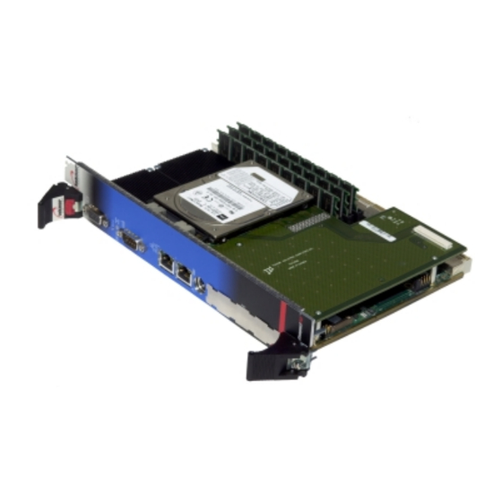
Mezzanine Cards (PMC). A fully equipped cPCI-DMXS64GX board may appear as follows: 1.5.1. Kontron’s Mezzanine Concept This is Kontron’s concept to expand the I/O capability of the board. It is built around two connectors: • Mezzanine connector handling IDE and floppy disk drive signals. -
Page 24: Pmc Concept
PCI bus. It conforms to the ANSI/IEEE P1386.1 specification that defines Standard Physical and Environmental Layers for PMC devices. The cPCI-DMXS64GX features the PMC concept onboard to provide an extra method to support the 32-bit I/O devices available on the market. -
Page 25: Onboard Features
2. ONBOARD FEATURES COMPACTFLASH INTERFACE ENHANCED IDE INTERFACES ETHERNET INTERFACES FLOPPY DISK INTERFACE PS/2 KEYBOARD AND MOUSE INTERFACES PARALLEL PORT POWER MANAGEMENT SCSI INTERFACE SERIAL PORTS THERMAL MANAGEMENT USB INTERFACES VIDEO INTERFACES... -
Page 26: Setups
(typical M.T.B.F. is 1,000,000 hours) and low power. The cPCI-DMXS64GX supports all CompactFlash sizes presently available and future sizes when available. The C-Flash disk connects on the cPCI-DMXS64GX via the onboard Flash Disk connector. Related Jumpers cPCI-DMXS64GX: W8 to set the CompactFlash disk as master or slave. -
Page 27: Enhanced Ide Interfaces
Technical Reference Manual 2.2. ENHANCED IDE INTERFACES The board features two channel Bus Master PCI EIDE dedicated to Primary and Secondary IDE logical interfaces. Each channel supports up to two IDE devices (including CD-ROMs, hard disks, plus CompactFlash on the secondary IDE interface) with independent timings, in Master/Slave combination. -
Page 28: Ethernet Interfaces
Feature Description 2.3. ETHERNET INTERFACES Both Ethernet controllers reside on the Primary PCI bus. Each interface supports 10Base-T and 100Base-TX specifications: 10Mbps and 100Mbps network speeds are automatically detected and switched. Signal Path See note on page 1.5. Related Jumpers None. -
Page 29: Cpci I/O Configuration
Technical Reference Manual 2.3.2. CPCI I/O Configuration Ethernet 1 and 2 signals are available on CPCI I/O connectors only when the board is ordered for rear access. ◊ CAUTION The combination of both front and rear panel configurations is not supported. -
Page 30: Ps/2 Keyboard And Mouse Interface
11.3.7 Integrated Peripherals : USB Keyboard Support; PS/2 Mouse Function Control 2.6. PARALLEL PORT The cPCI-DMXS64GX features one multi-mode parallel port. It is compatible with Standard Mode IBM PC/XT, PC/AT, and PS/2 compatible bi-directional parallel port, Enhanced Parallel Port (EPP), and Enhanced Capabilities Port (ECP). -
Page 31: Standard Mode
Technical Reference Manual The differences between Standard, EPP, and ECP modes appear in the signal assignation of the pins on the connector. Differences are described as follows: Pin Number (J5) Standard Mode EPP Mode ECP Mode SLCT SLCT PERROR... -
Page 32: Ecp Mode
Feature Description EPP mode assumes that the parallel port can be used to connect more than one peripheral device using multiplexor or daisy chain configurations. A multiplexor is an external device that permits up to eight parallel port devices to share a single parallel port. -
Page 33: Serial Ports
Technical Reference Manual Signal Path SCSI interface signals are only available through the J3-J4 CPCI I/O connector or through RTM (Rear Transition Module). Related Jumpers W4 – To determine the SCSI termination (hardware, software or disabled) BIOS Settings 11.3.7 Integrated Peripherals: Enable/Disable the Onboard PCI SCSI Chip. -
Page 34: Serial Port 1
Select Com Port Address of Serial Port 1 2.9.1.1. Remote Reset A remote hardware reset of the cPCI-DMXS64GX is possible by sending a break on the Serial Port 1 or Serial Port 2 (see section 3.1 for Remote Reset jumper setting). A break is simple an abnormally long start bit (100ms or more) on the incoming data line. -
Page 35: Front Plate Configuration
Technical Reference Manual The remote reset will work in RS-232 and RS-422 modes. It will also work with a modem, since the modem will repeat the break signal over the telephone network. All major telecommunication software have the capability of sending a break signal, usually by pressing the CTRL-B keys or the ALT-B keys on the keyboard. -
Page 36: Serial Port 3
Feature Description 2.9.3. Serial Port 3 The Serial Port 3 supports Infrared, RS-232, RS-422, and RS-485 operation modes. When assigned as Serial Port 3, the port is 100% compatible with the IBM-AT serial port in RS-232 mode. RS-422 and RS-485 modes allow communication using differential signals through one pair of wires (RS-485) or two (RS-422) to increase the noise immunity during data transfers. - Page 37 Technical Reference Manual Upon a power-up or reset, the Serial Port 3 interface circuits are automatically configured for the operation mode setup in the BIOS. The Serial Port 3 signal assignation on the J5 CPCI I/O connector depends on the operation mode (RS-232, RS-422, or RS-485) it has been set:...
-
Page 38: Infrared Mode
Feature Description 2.9.3.1. Infrared Mode Infrared (IR) interface signals are provided to drive IR module for remote operations through Serial Port 3. When set in IR mode, the IR interface supports multi-protocol infrared operations. The IR interface is IrDA 1.1 compliant, and supports TEMIC/HP modules, SHARP ASK IR, and consumer IR. -
Page 39: Thermal Management
Technical Reference Manual ◊ CAUTION When installing the cPCI-DMXS64GX at one end of the network, W6 and jumper caps must be installed to connect the 120 ohms termination resistors (see Section 3.1 – Setting Jumpers). 2.10. THERMAL MANAGEMENT Two temperature sensors are provided to supervise the thermal environment. One is used to monitor the CPU die temperature, while the second one, located on the CPU casing, allows the monitoring of the ambient temperature around the CPU. -
Page 40: Usb Interfaces
Feature Description The temperature management consists in reducing the CPU clock speed throttling when the temperature goes over the high limit (overheating condition) and suspending the throttling operation as soon as the temperature returns under the low temperature limit (normal condition). -
Page 41: Video Interface
USB supports Plug and Play and hot swapping operations (OS level). These user-friendly features allow USB devices to be automatically attached, configured and detached, without reboot or running setup. The cPCI-DMXS64GX board fully supports the standard universal host controller interface (UHCI) and uses standard software drivers that are UHCI-compatible. 2.12. VIDEO INTERFACE The high-performance video capability of the board is based on Accelerated Graphics Port (AGP) technology. -
Page 42: Supported Resolutions
Feature Description 2.12.1. Supported Resolutions The maximum video resolution and performance depend directly on the drivers running with your software application. Resolution and number of colors specification are listed below: Resolution Number of Colors 640x480, 800x600, 1024x768, 1280x1024 256 (8 bits) 640x480, 800x600, 1024x768 65,536 (16 bits) 640x480, 800x600... -
Page 43: Installing The Board
3. Installing the Board SETTING JUMPERS REGISTER’S DESCRIPTION ONBOARD INTERCONNECTIVITY CUSTOMIZING THE BOARD BUILDING A CPCI SYSTEM CPCI I/O SIGNALS... -
Page 44: Setting Jumpers
3.1. SETTING JUMPERS 3.1.1. Jumper Description for the PCI-DMXS64GX Description Onboard Battery Connects or Disconnects the battery to/from the board circuitry. Board Configuration Defines if used with Front Access or Rear Access Remote Reset To select Serial Port 1 or Serial Port 2 as a source for the remote hardware reset. -
Page 45: Cpci-Dmxs64Gx - Jumper Settings
Technical Reference Manual 3.1.2. PCI-DMXS64GX – Jumper Settings W1 Battery Board Configuration Rear Access Front Access 8HP Configuration 4HP Configuration PCI AGP Controller CompactFlash W8 Compact Flash Disk Master Slave W6, W7 COM2 Terminations RS-422/485 modes only With termination... -
Page 46: Register's Description Rs232/Rs485
Installing the Board 3.1.3. Register’s description RS232/RS485 CPLD Address READ n90h* RS485 RS232 WRITE n90h* RS485 RS232 Power-up Default : Enable RTS2 to be used as 485TX ENABLE when in 485 mode RS232 : Enable UART2 RS232 operation RS485 : Enable UART2 RS422 and 485 operation The serial port 2 mode can be controlled by setting three bits. -
Page 47: Multimedia, History Status
Technical Reference Manual 3.1.5. Multimedia, History status CPLD Address READ n92h* WD_LOCK CLRHIS WRITE n92h* WD_LOCK CLRHIS Power-up Default CLRHIS : When low, clear all history bits. Put this bit to 1 to enable history logging. WD_LOCK : When high, lock the state of the enable bit for the digital watchdog 3.1.6. -
Page 48: Digital Watchdog
Installing the Board The serial port 3 interrupt can be controlled in the following way. Bit 1 Bit 0 IRQ 3 IRQ 4 IRQ 5 IRQ 7 The serial port 3 base address can be controlled in the following way. CBAS Bit 1 Bit 0... -
Page 49: Nmi Control
Technical Reference Manual The digital watchdog duration can be controlled in the following way. WDD[2..0] NMI(T) RESET(T) NMI(T)+8T NMI(T)+8T 256T NMI(T)+8T 1024T NMI(T)+8T 4096T NMI(T)+8T 16384T NMI(T)+8T 65536T NMI(T)+8T 262144T NMI(T)+8T Time-out selection with T = 1.08ms (TBC) 3.1.9. NMI control... -
Page 50: Register Bits Description (Summary)
Installing the Board 3.1.10. Register BITs description (summary) Address CPLD READ n90* RS485 RS232 WRITE READ PBRST n91* WRITE READ n92* _CLRHIS WD_LOCK WRITE READ n93* IDCHIP I2C_DATA I2C_CLK WRITE READ n94* _CND3 CIS3_1 CIS3_0 CBAS3_1 CBAS3_0 RESERVED WRITE READ RESERV. -
Page 51: Onboard Interconnectivity
Technical Reference Manual 3.2. ONBOARD INTERCONNECTIVITY 3.2.1. cPCI-DMXS64GX Block Diagram XTAL ITP Test Early Power Connector Switching Clocks System Clock Regulators Hot Swap Synthes. & Controller Buffers V Cores GTL+ SMBus SVGA Intel 82443BX North Bridge Arbiter 492PBGA 21154 PCI- 3.3V, 33MHz Primary PCI Bus... -
Page 52: Mobile Pentium ® Ii / Iii Processor
Installing the Board The cPCI-DMXS64GX is not only a matter of computation power. The boards also provide a high capability to interface with peripherals through three integrated chips: Host-to-PCI bridge for. 443GX from Intel: interface with the processor (host), system memory, video controller, and Primary PCI bus (3.3V / 33MHz). -
Page 53: 82371Ab Pci-To-Isa Bridge / Ide Xcelerator (Piix4)
Technical Reference Manual The PCI-to-PCI bridge allows the Primary and Secondary PCI buses to operate concurrently. This means that a master and a target on the same PCI bus can communicate while the other PCI bus is busy. This traffic isolation may increase system performance in applications where system resources are highly used. -
Page 54: Onboard Connectors And Headers
Mezzanine RJ-45 connectors with built-in activity and link Ethernet 1, 2 J12, J10 indicators. This connector is dedicated to the Kontron’s CompactFlash CompactFlash module to support CompactFlash disk. Mouse and keyboard signals are combined on a Keyboard/Mouse standard 6-pin DSUB female connector. -
Page 55: Front Plate Connectors And Indicators
Technical Reference Manual 3.2.7. Front Plate Connectors and Indicators Name Description Comments Video Connector Standard 15-pin DSUB female connector Reset Button Use a small tool to press the button and proceed to a hardware reset of the board IDE/SCSI LEDs... -
Page 56: Faceplate Options
Installing the Board 3.2.8. FACEPLATE OPTIONS 4HP Front 4HP Rear 8HP Front 8HP Front 8HP Rear 8HP Rear Access with with 3.13... -
Page 57: Compactpci Connectors
CPCI J3 Connector Supports serial ports 2 (Infrared) and 3, V-Port, Ethernet2, and power signals. CPCI J2 Connector (P2 on the cPCI-DMXS64GX) Supports additional system slot signals, PCI 64-Bit extension, and power. CPCI J1 Connector (P1 on the cPCI-DMXS64GX) Supports CPCI bus signals, and power. -
Page 58: Customizing The Board
3.3. CUSTOMIZING THE BOARD 3.3.1. Processor and Fan cPCI-DMXS64GX Your board will be installed with the Mobile Pentium III processor, Low Power 500MHz and its adequate cooling system. Since CPUs are very sensitive components, particular attention should be given while installing a processor on the board. -
Page 59: Backup Battery
Technical Reference Manual 3.3.2. Backup Battery An onboard 3.6V lithium battery is provided to backup BIOS setup values and the real time lock (RTC). When replacing, the battery must be connected as follows: 3.6V Lithium Battery Positive Pin (Center) -
Page 60: Memory
Installing the Board 3.3.3. Memory 3.3.3.1. SDRAM System Memory The cPCI-DMXS64GX supports three 168-pin DIMM (Dual In-Line Memory Module) sockets for memory configuration from 256MB to 1.5GB of Synchronous DRAM in 4HP configuration and from 64MB to 1.5GB in 8HP configuration. -
Page 61: Dimm Installation
Technical Reference Manual 3.3.3.2. DIMM Installation NOTE If a Mezzanine card is installed, it must be removed before installation of DIMMs To install the DIMMs in the sockets, proceed as follows: 1. With the board flat on the table, turn it so that the front plate is facing you. -
Page 62: Supervision Features
Installing the Board 3.3.4. Supervision Features The cPCI-DMXS64GX provides a set of programmable I/O registers to setup the Intel PIIX4 (I/O addresses 4030h to 4037h) and the XILINX FPGA (I/O addresses programmable at 190h-193h, 290h-293h or 390h-393h using the AWARD Chipset Features Setup). -
Page 63: Watchdog
This feature is useful in embedded systems where human supervision is not required or impossible. The cPCI-DMXS64GX provides a two-stage digital watchdog with software programmable time-out period. Following a reset of any source, the watchdog is disabled. The watchdog can be enabled by software. - Page 64 Installing the Board A variable refresh is possible as shown below: Write to Register n96h with WDS[2,0] having the value below WatchD og internal counter value 16ms 8.6ms 8.6 ms RESET The programmable watchdog can be viewed as a decrementing counter that is initialized by a write to register n92h.
-
Page 65: Thermal Management
Technical Reference Manual TIME-OUT The programmable watchdog has two stages: the first stage has a variable time-out while the second stage has a fixed one. The first stage time-out is chosen at runtime from eight preset values (see table below). The first stage time-out generates an NMI interrupt (if enabled in register n92h). -
Page 66: Building A Cpci System
Installing the Board 3.4. BUILDING A CPCI SYSTEM When building a CompactPCI system, a minimum requirement consists in: a chassis, a CompactPCI backplane, a storage module, a power supply unit, and a ventilation system. The main AC power is drawn to the chassis components through an IEC power plug with a 2-stage filter, fuse holder and power switch. -
Page 67: Backplane
Technical Reference Manual 3.4.1. Backplane An entry-level backplane is provided by Kontron. It is referred to as cBP-08R. It features 8 CPCI slots (one PCI I/O segment), and includes J3-J5 I/O connectors on all slots. A 16-CPCI-slot backplane (cBP-16R) is also available from Kontron. It supports two PCI... -
Page 68: Rear-Panel I/O
Installing the Board 3.4.2. Rear-Panel I/O This feature is intended to issue the I/O capabilities of the system processor to the rear of the enclosure using a Rear I/O Transition module (cTM80-STD2S). The Rear I/O Transition module gathers all the I/O signals of the CPU board and makes them easily accessible through standard headers and connectors located at the rear of enclosure. - Page 69 Technical Reference Manual Rev. 3.26...
-
Page 70: Storage Devices
The ventilation unit of the enclosure conforms to the global requirement of the system in fully loaded configuration. 3.4.6. Installing the Board into a Bay The cPCI-DMXS64GX is mechanical Eurocard form factor boards. It takes advantages of the IEEE1101.10 specifications that ensure a mechanical interchange capability between different plug-in elements in sub-racks. -
Page 71: Connector Keying
Color coded keys prevent inadvertent installation of a 5V peripheral board in a 3.3V slot. The cPCI-DMXS64GX is universal. It does not support coding key. The PCI bus does not require to be keyed. Backplane connectors must always be keyed according to the signaling (VIO) level. -
Page 72: Bus Mastering
Installing the Board 3.4.8. Bus Mastering The cPCI-DMXS64GX provides seven pairs of REQ/GNT (0-6) arbitration signals through the Secondary PCI bus. This means the board is capable of driving up to seven CPCI slots with PCI Bus Master capabilities. 3.4.9. Connection To install the cPCI-DMXS64GX board into a bay, proceed as follows: 1. -
Page 73: Cpci I/O Signals
Technical Reference Manual 3.5. CPCI I/O SIGNALS This section describes integrated feature signals available on rear panel CPCI I/O connectors (J3, J4, and J5) 3.5.1. J3 Signal Specification 3.5.1.1. Ethernet LEDS Signal Pin Assignation Description SPEEDLED 0-1 A6, E6... -
Page 74: Serial Port 3
Installing the Board 3.5.1.3. Serial Port 3 Signal Pin Assignation Description COM3:DCD Data Carrier Detect COM3:RXD Receive Data COM3:DSR Data Set Ready COM3:TXD Transmit Data COM3:RTS Ready To Send COM3:CTS Clear To Send COM3:RI Ring Indicator COM3:DTR Data Terminal Ready 3.5.1.4. -
Page 75: Hot Swap Ha (High Availability) Signals
Technical Reference Manual 3.5.1.5. Hot Swap HA (High Availability) signals Signal Pin Assignation Description A15, B15, E15, D19 Board Select, one of the shortest pins (the last to BDSEL S2-S5 mate and the first to break contact). HEALTHY S2-S4... -
Page 76: J4 Signal Specification
Installing the Board 3.5.2. J4 Signal Specification 3.5.2.1. Power Management Signal Pin Assignation Description I2C-CLK I2C clock signal I2C-DATA I2C data signal Reserved EXT_FAN0_FAIL# Enclosure fan 0 fail EXT_FAN1_FAIL# Enclosure fan 1 fail SM_BYPASS# Reserved 3.5.2.2. SCSI Interface Signal Pin Assignation Description E7, D7, C7, B7, A7, SCSI Data –... -
Page 77: Video Interface
Technical Reference Manual 3.5.2.3. Video Interface Signal Pin Assignation Description VGA:SDA Video serial data line (video I2C) VGA:SCL Video serial clock line (video I2C) VGA:HSYNC Horizontal sync line VGA:VSYNC Vertical sync line VGA:RED Analog Red video signal VGA:GREEN Analog Green video signal... -
Page 78: Ide 1 Interface
Installing the Board 3.5.2.6. IDE 1 Interface Signal Pin Assignation Description IDE1:RESET# B20, E19, C19, A19, Sec. Disk Data – These signals are used to transfer D18, B18, E17, C17, data to or from the IDE device. IDE1: D0-D15 D17, A18, C18, E18, B19, D19, A20, C20 Sec. -
Page 79: J5 Signal Specification
Technical Reference Manual 3.5.3. J5 Signal Specification 3.5.3.1. IDE 0 Interface Signal Pin Assignation Description IDE0:RESET# Reset IDE0:RESET# Reset B4, E3, C3, A3, D2, B2, E1, C1, D1, A2, Prim. Disk Data – These signals are used to transfer... -
Page 80: Usb 0 And 1 Interfaces
Installing the Board 3.5.3.2. USB 0 and 1 Interfaces Signal Pin Assignation Description USB1:D+ B18, C18, D19, E19 USB Data – Differential data path for USB 0 and 1 ports D18, B19 USB Ground – Differential ground reference for USB 0 USB0, 1:GND and 1 ports E18, C19... -
Page 81: Serial Port 1
Technical Reference Manual 3.5.3.5. Serial Port 1 Signal Pin Assignation Description COM1:DCD Data Carrier Detect COM1:RXD Receive Data COM1:DSR Data Set Ready COM1:TXD Transmit Data COM1:RTS Ready To Send COM1:CTS Clear To Send COM1:RI Ring Indicator COM1:DTR Data Terminal Ready... -
Page 82: Parallel Port
Installing the Board 3.5.3.6. Parallel Port Signal Pin Assignation Description LPT:SELECT Printer select LPT:PE Paper end LPT:BUSY Busy signal LPT:ACK Acknowledge handshake E17, C17, A17, D16, LPT:D0-D7 Parallel port data bus C16, B16, A16, E15 LPT:SLCTIN# Printer select LPT:AUTOFEED# Auto line feed LPT:INIT# Initiate output LPT:ERROR#... -
Page 83: Software Setups
4. SOFTWARE SETUPS BIOS SETUP PROGRAM UPDATING OR RESTORING THE BIOS IN FLASH VT100 MODE... -
Page 84: Accessing The Bios Setup Program
4.1.1 Accessing the BIOS setup program The system BIOS (Basic Input Output System) provides an interface between the operating system and the hardware of the cPCI-DMXS64GX system processor. The CPCI- DMXS64GX and uses the AWARD Setup program, a setup utility in flash memory that is accessed by pressing the DELETE key at the appropriate time during system boot. - Page 85 Software Setups The main menu of the AWARD BIOS CMOS Setup Utility appears on the screen. Kontron T6007 BIOS VERSION 2.0 CMOS SETUP UTILITY AWARD SOFTWARE, INC. (2A69TU00) STANDARD CMOS SETUP LOAD BIOS DEFAULTS BIOS FEATURES SETUP LOAD SETUP DEFAULTS...
-
Page 86: Main Menu
Technical Reference Manual 4.1.2 Main Menu The Main Menu includes the following categories: Category Description Standard CMOS Setup This Setup page includes all the items in a standard, AT-compatible BIOS (date, time, hard disk type, floppy disk type, video adapter type, memory…). -
Page 87: Setups
Software Setups 4.1.3 Setups The arrow keys (↑ ↓ → ←) are used to highlight items on the menu and the PAGEUP and PAGEDOWN keys are used to change the entry values for the highlighted item. To enter in a submenu, press the ENTER key. Also, you can press the F1 key to obtain help information or the ESC key to close a menu or to quit the program. -
Page 88: Standard Cmos Setups
Hard Disks Two IDE controllers are defined on the cPCI-DMXS64GX board. The Primary and Secondary controllers can both have two disks: Master Disk or Slave Disk. Only three settings are available for the hard disk type: Auto, User and None. Type 1 to 46 are not predefined in the system: Use auto-detect or enter the parameters for the type in the user-defined. -
Page 89: Bios Features Setup
Software Setups 4.1.6 BIOS Features Setup BIOS Possible Option Setup Defaults Description Defaults Settings Virus Warning Dis. Dis. En. / Dis. When Enabled, you receive a warning message if a program (specifically, a virus) attempts to write to the boot sector or the partition table of the hard disk drive. - Page 90 Technical Reference Manual BIOS Features Setup (Continued) BIOS Setup Possible Option Description Defaults Defaults Settings Report No FDD For Yes, No Select Yes to release IRQ6 when the system contains no floppy Win 95 drive, for compatibility with Windows 95 logo certification. In the Integrated Peripherals screen, select NO on the Onboard FDC Controller option.
-
Page 91: Chipset Features Setup
CPU L2 Cache ECC Dis. En./Dis. Enables or Disables ECC Checking for L2 cache. Checking Note: processors provided by Kontron support ECC. However, not all Pentium® II / III processors support ECC. Check Intel’s website to know if your processor supports ECC: http://developer.intel.com/support/ processors/pentiumII/identify.htm. - Page 92 Technical Reference Manual Chipset Features Setup (Continued) BIOS Setup Possible Option Description Defaults Defaults Settings PCI/VGA Palette Dis. Dis. En./Dis. Palette snooping allows multiple VGA devices operating on Snoop different buses to handle data from the CPU on each set of palette registers.
-
Page 93: Power Management Setup
Software Setups 4.1.8 Power Management Setup This part of the setup configures power conservation options. BIOS Setup Possible Option Description Defaults Settings Defaults ACPI Function Dis. En./Dis. The Advanced Configuration and Power Interface (ACPI) allows Operating System Direct Power Management (OSPM) and make advanced configuration architectures possible. - Page 94 Technical Reference Manual Power Management Setup (Continued) BIOS Setup Possible Option Description Defaults Defaults Settings Resume by Ring Dis. En./Dis. When Enabled and a modem is connected to a serial port, allows a modem ring to re-activate the CPU when in Suspend mode.
-
Page 95: Pnp/Pci Configuration
Software Setups 4.1.9 PnP/PCI Configuration This part of the setup configures PnP/PCI options. BIOS Setup Possible Option Description Defaults Defaults Settings PNP OS Installed Yes, No If the operating system (OS) is Plug and Play (for example Windows 95), select “Yes” if you want the OS to allocate resources according to Plug and Play standards, or “No”... -
Page 96: Cpu/Board Features Setup
Technical Reference Manual 4.1.10 CPU/Board Features Setup BIOS Setup Possible Option Description Defaults Defaults Settings Current Processor(s) This option displays the current processor speed. Speed Front Side Bus Speed This option displays the current Front Side Bus speed. This speed is selected by the CPU auto-detection logic. -
Page 97: Integrated Peripherals
Software Setups 4.1.11 Integrated Peripherals Option BIOS Setup Possible Description Defaults Defaults Settings Select Enabled to activate the Primary/Secondary IDE On-Chip Primary/Secondary En./Dis. channel. The four options below appear only if the On-Chip Primary option is enabled. On-Chip Primary IDE Use this option to set a PIO mode (0-4) for each of the onboard IDE devices. -
Page 98: Vt100 Mode
Technical Reference Manual 4.2. VT100 MODE The VT100 operating mode allows remote setups of the board. This configuration requires a remote terminal that must be connected to the board through a serial communication link. 4.1.12 Requirements The terminal should emulate a VT100 or ANSI terminal. Terminal emulation programs such ®... -
Page 99: Running Without A Terminal
Software Setups 4.1.14 Running Without a Terminal The board can boot up without a screen or terminal attached. If the speed is set to Auto and no terminal is connected, the speed is set to 115,200 bauds. Furthermore, you can run without any console at all by simply not enabling VT100 Mode and by disabling the onboard video. - Page 100 APPENDICES BOARD SPECIFICATIONS MEMORY & I/O MAPS INTERRUPT LINES BOARD DIAGRAMS CONNECTOR PINOUTS BIOS SETUP ERROR CODES EMERGENCY PROCEDURE GETTING HELP & RMA...
-
Page 101: Board Specifications
Proprietary Mezzanine with PCI bus, FD and EIDE support SMBus (for power management of CPU temperature monitoring, DRAM control, clock buffers and power control) cPCI-DMXS64GX: Level 1: 16/16KB instruction/Data CPU-internal Level Cache Memory Level 2: 256KB internal, 64-bit wide, pipelined burst... - Page 102 Technical Reference Manual Board Specifications (continued) Real-time clock with (replaceable) battery backup, CMOS RAM Clock/Calendar Connectors in “Front” Front Plate configuration 15-pin D-Sub COM1 9-pin D-Sub Ethernet 1 and 2 2 x RJ-45 with built-in LEDs PS/2 mouse + Keyboard...
- Page 103 Board Specifications Two-stage software programmable Watchdog timer drives NMI on 1 Supervisory stage and system reset on 2 stage. Programmable CPU temperature monitor/alarm Power failure/low battery detector Front Panel LED : IDE activity and SCSI activity, Hot Swap, Ethernet and link activity MS-DOS™, Windows®...
- Page 104 Technical Reference Manual Board Specifications (continued) Operating Storage and Transit Environmental Temperature 0-60°C / 32-140°F -40 to +70°C / -40 to 158°F Humidity 5% to 95% @ 40°C/104°F 5% to95% @ 40°C/104°F non-condensing non-condensing Altitude 4,572m / 15,000 ft...
-
Page 105: Memory & I/O Maps
B. MEMORY & I/O MAPS EMORY APPING FFFFFh System BIOS E0000h 1MB to top of DRAM Optional ROM (Free) LAN BIOS if activated (~30KB) See Note 1 See Note 2 SCSI BIOS (18KB at runtime) Optional ROM (Free) C 000h Video BIOS C0000h 100000h... -
Page 106: I/O Mapping
Technical Reference Manual I/O M APPING Address Optional Optional Optional Function Address Address Address 000-01F DMA Controller 1 020-03F Interrupt Controller 1 040-05F Timer 060-06F Keyboard 070-07F Real-time clock 080-09F DMA Page Register 0A0-0BF Interrupt Controller 2 0C0-0DF DMA Controller 2... -
Page 107: Interrupt Lines
1 Available lines service on board and external PCI/ISA PnP devices or a Legacy ISA device. DMA C HANNELS The cPCI-DMXS64GX integrates the functionality of two 8237 DMA controllers. Eight DMA channels are available. According to Plug and Play standards, the system BIOS automatically allocates DMA Channel 1 or 3 for the parallel port's ECP mode. -
Page 108: Board Diagrams
D. BOARD DIAGRAMS EVICES URFACE OUNT... -
Page 109: Assembly Bottom Diagram
Technical Reference Manual SSEMBLY OTTOM IAGRAM... -
Page 110: Mounting Holes
Board Specifications OUNTING OLES... -
Page 111: Connector Holes
Technical Reference Manual ONNECTOR OLES... -
Page 112: Connector Pinouts
Ethernet 2 Connector (Front panel configuration only) PCI Mezzanine Ethernet 1 Connector (Front panel configuration only) CompactFLASH Disk Connector J14-J16 DIMMs Keyboard/Mouse Connector Storage Mezzanine Connector Reserved J20, J21 Kontron’s Mezzanine Card Hot Swap Switch Reserved Reset Switch CMOS Battery Backup connector... -
Page 113: J1 Cpci Bus
Technical Reference Manual PCI B ROW A ROW B ROW C ROW D ROW E VCC5E -12VE +12VE VCCE VCCE INTA# INTB# INTC# VCCE INTD# IPMB_PWR HEALTHY# VI/O IRQ14 INTS RST# GNT0# REQ0# VCC3E CLK0 AD31 AD30 AD29 AD28... -
Page 114: J2 Cpci Bus
Connector Pinouts PCI B ROW A ROW B ROW C ROW D ROW E S_CLK1 REQ1# GNT1# REQ2# S_CLK2 S_CLK3 SYSEN# GNT2# REQ3# S_CLK4 GNT3# REQ4# GNT4# V I/O CBE7# CBE6# CBE5# V I/O CBE4# PAR64 AD63 AD62 AD61 AD60 AD59 V I/O AD58... -
Page 115: J3 Cpci Bus
Technical Reference Manual PCI B ROW A ROW B ROW C ROW D ROW E SCSI:D11+ SCSI:I/O+ SCSI:D9+ SCSI:DIFFSENS SCSI:D10+ SCSI:C/D+ SCSI:SEL+ SPEEDLED0 LAN0:LINK LAN0:ACT LAN1:LINK SPEEDLED1 LAN1:ACT LAN1:ETX+1 LAN1:ETX- LAN1:ERX+ LAN1:ERX- WR_80# +12V +12V COM3:DCD# COM3:RXD COM3:DSR# COM3:TXD... -
Page 116: J4 Cpci Bus
Connector Pinouts PCI B ROW A ROW B ROW C ROW D ROW E EXT_FAN0_FAI EXT_FAN1_FAI I2C:CLK I2C-DATA SM_BYPASS# SCSI:D11- SCSI:D10- SCSI:D9- SCSI:D8- SCSI:I/O- SCSI :REQ- SCSI:C/D- SCSI:SEL- SCSI:MSG- SCSI:RST- SCSI :ACK- SCSI:BSY- SCSI:BSY+ SCSI:ATN- SCSI:TERMPW SCSI:TERMPW SCSI:ACK+ N.C. SCSI:DP0- SCSI:ATN+ SCSI :DP0- SCSI:D7-... -
Page 117: J5 Cpci Bus
Technical Reference Manual PCI B ROW A ROW B ROW C ROW D ROW E BRSTDRV# IDE0:RESET# IDE0:D7 IDEO:D8 IDE0:D6 IDE0:D9 IDE0:D5 IDE0:D10 IDE0:D4 IDE0:D11 IDE0:D3 IDE0:D12 IDE0:D2 IDE0:D13 IDE0:D1 IDE0:D14 IDE0:D0 IDE0:D15 IDE0:IRQ14 IDE0:REQ IDE0:IORDY IDE0:IOW# IDE0:DACK# IDE0:IOR#... -
Page 118: J9, Serial Port 1
Connector Pinouts J9, S 1 - RS-232 ERIAL Pin Number Pin Number Top View Signal Signal RXD# TXD# J10/J12, E THERNET Top View Signal Yellow Note Not Connected These two LEDs Not Connected might be reversed. Green Not Connected Not Connected... -
Page 119: J11, Pci Mezzanine Card
Technical Reference Manual E.10 J11, PCI M EZZANINE Top View MS2_BD_SEL# PBRST# MS4_BD_SEL# MS2_HEALTHY# C/BE0# AD11 AD10 MS8_HEALTHY# AD14 AD13 AD12 VCC3 C/BE1# AD15 VCC3 SERR# MS4_HEALTHY# PERR# VCC3 MEZ_SDONE STOP# VCC3 LOCK# VCC3 TRDY# DEVSEL# FRAME# IRDY# VCC3... -
Page 120: J13, Compactflash Disk
Connector Pinouts E.11 J13, C OMPACT LASH Top View Pin Number Pin Number Signal Signal DD11 DD12 DD03 DD13 DD04 DD14 DD05 DD15 DD06 CS1# DD07 DMA ACK# CS0# DMA RQ D IOR# PDIAG# D IOW# IRQ14 VCC (+5V) VCC (+5V) VCC (+5V) RESET# C Select... -
Page 121: J18, Storage Mezzanine
Technical Reference Manual E.13 J18, S TORAGE MEZZANINE Top View IDE0:D0 MCLK MDATA IDE0:D1 IDE0:D2 KBDAT KBCLK IDE0:D3 IDE0:D4 VCC_KBD IDE0:D5 IDE0:D6 IDE0:D7 IDE0:D8 IDE0:D9 IDE0:D10 IDE0:D11 IDE0:D12 IDE0:D13 IDE0:D14 FD_DRVEN0# FD_DS1# IDE0:D15 BRSTDRV# FD_DRVEN1# FD_MTR1# DIOW# FD_INDEX# FD_DS0... -
Page 122: J20, Kontron's Mezzanine
Connector Pinouts E.14 J20, K ’ ONTRON EZZANINE Top View Pin Number Pin Number Signal Top View Signal Not Connected -12V INTA# INTB# INTC# BUSMODE1# INTD# Not Connected Not Connected PCLK GNT # REQ# AD31 AD28 AD27 AD25 CBE3# AD22 AD21 AD19 AD17... -
Page 123: J21, Pmc
Technical Reference Manual E.15 J21, PMC Top View Pin Number Pin Number Signal Top View Signal +12V Not Connected Not Connected Not Connected Not Connected Not Connected Not Connected Not Connected BUSMODE2# VCC3 PCIRST# BUSMODE3# VCC3 BUSMODE4# Not Connected... -
Page 124: J22, Hot Swap Switch
Connector Pinouts E.16 J22, H WITCH Top View Signal VCC3E SW_OPEN# E.17 S1 – R ESET WITCH View Signal RESET# E.18 BT1, CMOS B ATTERY ACKUP ONNECTOR Front View Signal Battery (+) Battery (-) E-13... -
Page 125: Bios Setup Error Codes
F. BIOS SETUP ERROR CODES POST B POST beep codes are defined in the BIOS to provide low level tone indication when an error occurs during the BIOS initialization. Beep codes consist of a combination of long and short beeps. They are described as follows: Beep Codes Post... -
Page 126: Error Messages
If it’s the first boot, check for the onboard battery jumper (jumper W4 for both the cPCI-DMXS64GX). The board is shipped with W4 jumper set to OFF (onboard battery disconnected). This jumper must be shorted (ON) for proper battery operation. -
Page 127: Post Codes
Test F000h segment shadow readable and writeable for POST access correct. If not, show POST FE and beep continuously… Autodetect Flash EPROM. Test CMOS Interface and Kontron Install the segment. Battery Status Verifies CMOS is working correctly (walking bit test). - Page 128 cPCI-MXS64GX Technical Reference Manual POST Codes (continued) POST # Designation Description Test CMOS RAM Checksum Verify time and date for valid values. If Override enabled, check for Override key. If Override key pressed, Kill CMOS checksum. Check CMOS Battery (useless if save CMOS in FLASH enabled since it’s already done).
- Page 129 BIOS Setup Error Codes POST Codes (continued) POST Designation Description Initialize Keyboard Open Xilinx I/O Port Boot Block 1 : Verify BIOS location to x90h (X=1,2 or checksum. 3) inside the chipset (if necessary). Disable (if necessary). Boot Block in EMERGENCY 2 Thermal Management.
- Page 130 cPCI-MXS64GX Technical Reference Manual POST Codes (continued) POST Designation Description Test Video Memory If CGA or MONO, test video memory. Beep the speaker. Show the LOGO. Install VT100 driver if necessary. Write sign-on message to screen. Write Copyright message to screen. Write Evaluation message to screen.
- Page 131 BIOS Setup Error Codes POST Codes (continued) POST Designation Description Size Base & Extended Memory Size base memory from 256K to 640K and extended memory above 1MB. Test Base & Extended Memory Test base memory from 256K to 640K and extended memory above 1MB using various patterns.
- Page 132 Put Num Lock ON and Daylight Saving. Boot Attempt Call POST 82. Set Low stack. Boot via int 19h. 64-7F Reserved Reserved Kontron Kontron Segment Move 1 Install the segment from Flash to DC00:0h. Kontron Kontron Segment Move 2 Install the segment from DC00:0h to 7000:0h.
- Page 133 BIOS Setup Error Codes POST Codes (continued) POST Designation Description Check & Program CPLD Check & Program CPLD for valid UserCode & IDCode. Kontron Kontron CRC Check Check if block have a valid CRC. If not, the Emergency procedure is launched. 85-AF...
- Page 134 cPCI-MXS64GX Technical Reference Manual POST Codes (continued) POST Designation Description Power Management – Suspend Trying to go or in Suspend mode. mode D4-DF Debug Available POST codes for use by source code customers during development. Reserved Reserved E1-EE Setup Page Page 1 to Page 14 Shadow Error In POST 6 to signal a Shadow Error.
-
Page 135: Emergency Procedure
G. EMERGENCY PROCEDURE Follow this procedure only in case of emergency such as a critical error occurred during the Boot Block Flash BIOS update (when using UBIOS utility program or if you meet one of the following symptoms at anytime: No POST code on a power up (when using a POST card). -
Page 136: Generate An Emergency Floppy Diskette
LOPPY ISKETTE Use a system that has a 1.44 Mbytes floppy drive A. Insert the Kontron Emergency Diskette in drive A: Copy the two files WDISK.COM and EMERDISK.TEK to your hard drive (those files are available from the driver’s CDROM). -
Page 137: Getting Help
Technical Support department at: CANADIAN HEADQUARTERS Tel. (450) 437-5682 Fax: (450) 437-8053 If you have any questions about Kontron, our products or services, you may reach us at the above numbers or by writing to : Kontron Communications inc. 616 Curé Boivin Boisbriand, Québec... - Page 138 Technical Reference Manual Returning Defective Merchandise If your Kontron product malfunctions, please do the following before returning any merchandise: 1) Call our Technical Support department in Canada at (450) 437-5682. Make certain you have the following at hand: •...
- Page 139 : ___________________ Postal/Zip Code: _______________ Phone Number : ___________________ Extension : ___________________ Fax Number : __________________ P.O. # Serial Number Failure or Problem Description (if not under warranty) Fax this form to Kontron’s Technical Support department in Canada at (450) 437-8053...
Need help?
Do you have a question about the cPCI-DMXS64GX and is the answer not in the manual?
Questions and answers