Table of Contents
Advertisement
Quick Links
Advertisement
Table of Contents

Related Manuals for Kontron cPCI-MXS64


Summary of Contents for Kontron cPCI-MXS64
- Page 1 ® 6U CompactPCI 64-bit System Processor Technical Reference Manual Version 1.4, February 2003 Note: The latest releases of the Technical Reference Manuals are available at: ftp://ftp.kontron.ca/Support/Product_Manuals/ www.kontron.com Ref. : M6002_TECH...
- Page 2 FCC Compliance Statement Warning Changes or modifications to this unit not expressly approved by the party responsible for the compliance could void the user’s authority to operate this equipment. This equipment has been tested and found to comply with the limits for a Class A digital device, pursuant to Part 15 of the FCC rules.
- Page 3 This document may contain information or refer to products protected by the copyrights or patents of others and does not convey any license under the patent rights of Kontron, nor the rights of others. Printed in Canada.
- Page 4 _______________________________________________________________________________________ Additional comments (any changes or modifications to this manual): _______________________________ _______________________________________________________________________________________ ______________________________________________________________________________ Optional Please send your comments to: Name ________________________________ Kontron Inc Company _____________________________ Technical Writing dept. Address ______________________________ _____________________________________ 616 Curé Boivin, Boisbriand _____________________________________ (Québec) CANADA J7G 2A7...
- Page 5 ADDITIONAL COMMENTS...
- Page 6 READ ME FIRST Your computer board has a standard non-rechargeable lithium battery. To preserve the battery lifetime, the battery enable jumper is removed when you receive the board. If you do not have any jumper cap, we suggest you to use the Watchdog Timer jumper cap. EXERCISE CAUTION WHILE REPLACING LITHIUM BATTERY WARNING Danger of explosion if battery is incorrectly replaced.
- Page 7 ADAPTER CABLES While adapter cables are provided from various sources, the pinout is often different. The direct crimp design offered by Kontron allows the simplest cable assembly. All cables are available from Kontron Sales Department.
- Page 8 After opening the box, save it and the packing material for possible future shipment. Remove the board from its antistatic wrapping and place it on a grounded surface. Inspect the board for damage. If there is any damage, or items are missing, notify Kontron immediately. When unpacking you will find: ®...
-
Page 9: Table Of Contents
1.2. Product Specifications..................1-2 1.3. Hot Swap capability................... 1-4 1.4. Interfacing with the Environment ............... 1-6 1.4.1 cPCI ........................1-6 1.4.2 Mezzanine......................1-6 1.5. Compatibility with other KONTRON Products ........... 1-7 1.6. Mezzanine Card Concept.................. 1-8 1.6.1 Kontron’s Mezzanine Concept................1-9 1.6.2 PMC Concept......................1-9 1.6.3 CompactFlash Feature ..................1-9... - Page 10 2.5. PS/2 Keyboard / PS/2 Mouse Interface............. 2-4 2.6. Parallel Port....................... 2-5 2.6.1 Standard Mode....................2-6 2.6.2 EPP Mode ......................2-6 2.6.3 ECP Mode......................2-6 2.7. Power Management ..................2-7 2.8. SCSI Interface ....................2-7 2.9. Serial Ports......................2-8 2.9.1 SERIAL PORT 1....................2-8 2.9.1.1.
- Page 11 Uart 4 PnP Configuration..................3-5 3.1.9 Digital Watchdog ....................3-5 3.1.10 NMI Control ......................3-6 3.1.11 0Register BITs Description (Summary)..............3-7 3.2. Onboard Interconnectivity ................. 3-8 3.2.1 cPCI-MXS64 Block Diagram................3-8 ® 3.2.2 Mobile Pentium II / III Processor ................3-9 3.2.3 North Bridge Chipset ...................3-9 3.2.4...
- Page 12 3.3.4.2. Watchdog ....................3-20 3.3.4.3. Thermal Management .................3-22 3.4. Building a cPCI System................... 3-23 3.4.1 Backplane ......................3-24 3.4.2 Rear-Panel I/O ....................3-25 3.4.3 Storage Devices ....................3-27 3.4.4 Power Supply ....................3-27 3.4.5 Fan Tray......................3-27 3.4.6 Installing the Board into a Bay ................3-27 3.4.7 Connector Keying....................3-28 3.4.8 Bus Mastering ....................3-28...
- Page 13 3.5.3 J5 Signal Specification ..................3-34 3.5.3.1. IDE 0 Interface ..................3-34 3.5.3.2. USB 0 and 1 Interfaces................3-34 3.5.3.3. Floppy Disk Interface................3-35 3.5.3.4. Serial Port 2 ..................3-35 3.5.3.5. Serial Port 1 ..................3-35 3.5.3.6. Parallel Port..................3-36 3.5.3.7. Miscellaneous Signals .................3-36 3.5.3.8. Keyboard Interface ................3-36 3.5.3.9.
- Page 14 D.1 Top Devices Surface Mount..................D-1 D.2 Assembly Bottom Diagram ...................D-2 D.3 Mounting Holes ......................D-3 D.4 Connector Holes ......................D-4 CONNECTOR PINOUTS .......................E-1 cPCI-MXS64 Connectors and Headers ................. E-1 PCI Bus......................... E-2 PCI Bus......................... E-3 PCI Bus......................... E-4 PCI Bus......................... E-5 PCI Bus......................... E-6 J12, Video (VGA)......................
- Page 15 E.11 J18, CompactFlash Disk ....................E-8 E.12 J19, Storage mezzanine ....................E-9 E.13 J20, PMC........................E-10 E.14 J21, PMC........................E-11 E.15 Hot Swap Switch......................E-12 E.16 S1 – Reset Switch ...................... E-12 E.17 BT1, CMOS Battery Backup Connector ..............E-12 BIOS SETUP ERROR CODES ......................F-1 POST Beep ........................
-
Page 16: Product Description
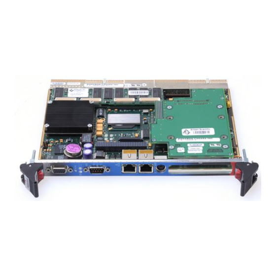
1. PRODUCT DESCRIPTION PRODUCT OVERVIEW PRODUCT SPECIFICATIONS HOT SWAP CAPABILITY INTERFACING WITH THE ENVIRONMENT COMPATIBILITY WITH KONTRON PRODUCTS MEZZANINE CARD CONCEPTS... - Page 17 Rear I/O cPCI connectors are PICMG 2.0 Rev 3.0 compliant. CompactPCI connectors are located at the rear edge of the processor board. The complete cPCI connector configuration of the cPCI-MXS64 is composed of four connectors referred to as J1, J2, J3, J4, and J5. Their function is described below: 32 bit PCI signaling, power 64 bit extension, arbitration, clocks, reset and.
-
Page 18: Product Specifications
The cPCI-MXS64 industrial system processor features: • ® Intel’s enhanced performance Pentium processor. cPCI-MXS64: low power Mobile Pentium®III 500 & 700MHz, 256KB on-die L2 pipelined burst cache. • 440BX AGP set. • Supporting up to 768 MB SDRAM with parity or ECC. - Page 19 • Two year warranty. The cPCI-MXS64 can be purchased either for front plate I/O interfacing (video serial port, Ethernet) or RTM (Rear Transition Module) I/O interfacing (no interconnection capability available on the front plate) through cPCI I/O connectors and backplane.
-
Page 20: Hot Swap Capability
Technical Reference Manual 1.3. HOT SWAP CAPABILITY The cPCI-MXS64 supports Hot Swap capability which means that hot swappable boards can be removed from or installed in the system while online (without powering-down the system). Hot Swap consists of board hardware with the Hot Swap additions to the Hardware Connection Layer, and the Hot-Plug Service. - Page 21 Product Description The Software Connection Control resources on the board provide a signal (ENUM#) for system host notification and a switch and LED to interface with the operator. Full Hot Swap boards drive the ENUM# signal to the system host to indicate a service request.
-
Page 22: Interfacing With The Environment
Passive Backplane. 1.4.2 Mezzanine The mezzanine is a hardware interface concept introduced by Kontron to increase the I/O connectivity of the cPCI-MXS64, but respecting the dual slot 6U form factor restrictions. The onboard mezzanine connector features PCI bus, IDE, floppy, keyboard and mouse signals, for potential mezzanine applications: Kontron provides an optional storage mezzanine composed with a hard drive, a floppy disk drive. -
Page 23: Compatibility With Other Kontron Products
Product Description 1.5. COMPATIBILITY WITH OTHER KONTRON PRODUCTS The cPCI-MXS64 System Processor is a member of the Kontron’s CompactPCI product family. The boards are fully compliant with the PICMG 2.0 Rev.2.1 and PICMG 2.1 CompactPCI specifications. When building a basic environment around the cPCI-MXS64, the platform may be composed of any of the following devices: •... -
Page 24: Mezzanine Card Concept
Technical Reference Manual 1.6. MEZZANINE CARD CONCEPT The capability of the cPCI-MXS64 to connect with other devices is enforced by PCI Mezzanine Cards (PMC). A fully equipped cPCI-MXS64 board may appear as follows:... -
Page 25: Kontron's Mezzanine Concept
Product Description 1.6.1 Kontron’s Mezzanine Concept This is Kontron’s concept to expand the I/O capability of the board. It is built around two connectors: • Mezzanine connector handling IDE and floppy disk drive signals. • Mezzanine connector handling a complete PCI signal set (primary bus) including the REQ/GNT arbitration signal pair. -
Page 26: Onboard Features
2. ONBOARD FEATURES COMPACTFLASH INTERFACE ENHANCED IDE INTERFACES ETHERNET INTERFACES FLOPPY DISK INTERFACE PS/2 KEYBOARD AND MOUSE INTERFACE PARALLEL PORT POWER MANAGEMENT SCSI INTERFACE SERIAL PORTS THERMAL MANAGEMENT USB INTERFACES VIDEO INTERFACES... -
Page 27: Setups
(typical M.T.B.F. is 1,000,000 hours) and low power. The cPCI-MXS64 supports all CompactFlash size presently available and future sizes when available. The C-Flash disk connects on the cPCI-MXS64 via the onboard Flash Disk connector. Related Jumpers cPCI-MXS64: W3 to set the CompactFlash disk as master or slave. -
Page 28: Enhanced Ide Interfaces
Technical Reference Manual 2.2. ENHANCED IDE INTERFACES The board features two channel Bus Master PCI EIDE dedicated to Primary and Secondary IDE logical interfaces. Each channel supports up to two IDE devices (including CD-ROMs, hard disks, plus CompactFlash on the primary IDE interface) with independent timings, in Master/Slave combination. -
Page 29: Ethernet Interfaces
Onboard Features 2.3. ETHERNET INTERFACES Both Ethernet controllers reside on the Primary PCI bus. Each interface supports 10Base-T and 100Base-TX specifications: 10Mbps and 100Mbps network speeds are automatically detected and switched. Signal Path See note on page 1.5. Related Jumpers None. -
Page 30: Floppy Disk Interface
The Boot from LAN capability is supported. To enable the option, use the BIOS Setup program. Please refer to Section 4.1 BIOS Setup Program. A diskette entitled “Network Drivers for Intel 82559 is included with the cPCI-MXS64. It contains network drivers for most common operating systems. -
Page 31: Parallel Port
Onboard Features 2.6. PARALLEL PORT The cPCI-MXS64 features one multi-mode parallel port. It is compatible with Standard Mode IBM PC/XT, PC/AT, and PS/2 compatible bi-directional parallel port, Enhanced Parallel Port (EPP), and Enhanced Capabilities Port (ECP). Signal Path The Parallel Port interface is only available through J5 cPCI I/O connector. -
Page 32: Standard Mode
Technical Reference Manual NOTE To operate in EPP or ECP mode, ensure the peripheral is designed to work in this mode and the BIOS setup is configured to support it. 2.6.1 Standard Mode The Standard mode is unidirectional. It is supported to maintain the compatibility with the IBM PC standard. -
Page 33: Power Management
Onboard Features NOTE For more information on the ECP protocol, please refer to the Extended Capabilities Port Protocol and ISA Interface Standard (available from Microsoft Corporation) or contact our Technical Support department. 2.7. POWER MANAGEMENT Power Management features are supported at the BIOS level. All Power Management options are described in Section 4.1.8 –... -
Page 34: Serial Ports
2.9.1.1. Remote Reset A remote hardware reset of the cPCI-MXS64 is possible by sending a break on the Serial Port 1 or Serial Port 2 (see Section 3.1 for Remote Reset jumper setting). A break is simple an abnormally long start bit (100ms or more) on the incoming data line. A break signal is... -
Page 35: Front Plate Configuration
Onboard Features Related Jumpers W5– Remote reset on Serial Port 1 or Serial Port 2 or disabled to select whether the serial port 1 or 2 is used to control the remote reset Bios Settings None The remote reset will work in RS-232 and RS-422 modes. It will also work with a modem, since the modem will repeat the break signal over the telephone network. -
Page 36: Serial Port 3
Technical Reference Manual 2.9.3 Serial Port 3 The Serial Port 3 supports Infrared, RS-232, RS-422, and RS-485 operation modes. When assigned as Serial Port 3, the port is 100% compatible with the IBM-AT serial port in RS-232 mode. RS-422 and RS-485 modes allow communication using differential signals through one pair of wires (RS-485) or two (RS-422) to increase the noise immunity during data transfers. -
Page 37: Infrared Mode
Onboard Features 2.9.3.1. Infrared Mode Infrared (IR) interface signals are provided to drive IR module for remote operations through Serial Port 3. When set in IR mode, the IR interface supports multi-protocol infrared operations. The IR interface is IrDA 1.1 compliant, and supports TEMIC/HP modules, SHARP ASK IR, and consumer IR. -
Page 38: Serial Port 4
Technical Reference Manual CAUTION When installing the cPCI-MXS64 at one end of the network, W8 and W9 jumper caps must be installed to connect the 120 ohms termination resistors (See Section 3.1 – Setting Jumpers). 2.9.4 Serial Port 4 The Serial Port 4 is buffered directly for RS-232 operations and is 16C550 PC-Compatible. -
Page 39: Usb Interfaces
USB supports Plug and Play and hot swapping operations (OS level). These user-friendly features allow USB devices to be automatically attached, configured and detached, without reboot or running setup. The cPCI-MXS64 board fully supports the standard universal host controller interface (UHCI) and uses standard software drivers that are UHCI-compatible. 2-13... -
Page 40: Video Interface
Technical Reference Manual 2.12. VIDEO INTERFACE The high-performance video capability of the board is based on Accelerated Graphics Port (AGP) technology. The video controller, Intel 69000, with its integrated 2Meg of high performance SDRAM is capable of CRT resolutions up to 1024 x 768 x 64K colors or 1280 x 1024 x 256 colors. -
Page 41: Major Features Description
Onboard Features 2.12.2 Major Features Description VGA Compatibility The video controller includes all registers and data paths required for VGA controller and supports extensions to VGA, including resolutions up to 800x600x16.8 million colors non-interlaced. The 16-bit images are displayed at up to 1024x768 resolution. 2D Graphics Engine The 2D graphics engine is an advanced 32-bit three-operand engine that accelerates BitBLTs as line draws, polygon draw, and polygon fill. -
Page 42: Installing The Board
3. INSTALLING THE BOARD SETTING JUMPERS REGISTER’S DESCRIPTION ONBOARD INTERCONNECTIVITY CUSTOMIZING THE BOARD BUILDING A cPCI SYSTEM cPCI I/O SIGNALS... -
Page 43: Setting Jumpers
3.1. SETTING JUMPERS 3.1.1 Jumper Description for the PCI-MXS64 Description VT-100 Mode (1-2) When enabled, allows VT100 or ANSI terminal connection Download Mode (3-4) When enabled, allows data serial download from a remote computer. Board Configuration Defines if used with Front Access or Rear Access CompactFlash Setting Use this connector to setup the CompactFlash... -
Page 44: Cpci-Mxs64 - Jumper Settings
Technical Reference Manual 3.1.2 PCI-MXS64 – Jumper Settings W4 Battery Connected Disconnected W3 Compact Flash Disk Master Slave Board Configuration Rear Access Front Access W1 VT-100 / Download Mode 8HP Configuration Enable VT-100 mode Reserved * Default Setting 4HP Configuration... -
Page 45: Register's Description Rs232/Rs485
Installing the Board 3.1.3 Register’s Description RS232/RS485 CPLD Address READ n90h* RS485 RS232 WRITE n90h* RS485 RS232 Power-up Default : Enable RTS2 to be used as 485TX ENABLE when in 485 mode RS232 : Enable UART2 RS232 operation RS485 : Enable UART2 RS422 and 485 operation The serial port 2 mode can be controlled by setting three bits. -
Page 46: Multimedia, History Status
Technical Reference Manual 3.1.5 Multimedia, History Status CPLD Address READ n92h* WD_LOCK CLRHIS WRITE n92h* WD_LOCK CLRHIS Power-up Default CLRHIS : When low, clear all history bits. Put this bit to 1 to enable history logging. WD_LOCK : When high, lock the state of the enable bit for the digital watchdog 3.1.6 Monitoring Status and I/O Access... -
Page 47: Uart 4 Pnp Configuration
Installing the Board The serial port 3 & 4 interrupt can be controlled in the following way. Bit 1 Bit 0 IRQ 3 IRQ 4 IRQ 5 IRQ 7 The serial port 3 & 4 base address can be controlled in the following way. CBAS Bit 1 Bit 0... -
Page 48: Nmi Control
Technical Reference Manual The digital watchdog duration can be controlled in the following way. WDD[2..0] NMI(T) RESET(T) NMI(T)+8T NMI(T)+8T 256T NMI(T)+8T 1024T NMI(T)+8T 4096T NMI(T)+8T 16384T NMI(T)+8T 65536T NMI(T)+8T 262144T NMI(T)+8T Time-out selection with T = 1.08ms (TBC) 3.1.10 NMI Control... -
Page 49: 0Register Bits Description (Summary)
Installing the Board 3.1.11 0Register BITs Description (Summary) Address CPLD READ n90* RS485 RS232 WRITE READ PBRST n91* WRITE READ n92* _CLRHIS WD_LOCK WRITE READ n93* IDCHIP I2C_DATA I2C_CLK WRITE READ n94* _CND3 CIS3_1 CIS3_0 CBAS3_1 CBAS3_0 RESERVED WRITE READ RESERV. -
Page 50: Onboard Interconnectivity
Technical Reference Manual 3.2. ONBOARD INTERCONNECTIVITY 3.2.1 cPCI-MXS64 Block Diagram XTAL Intel Pentium III ITP Test Early Power Connector Switching Clocks MPIII Core Hot Swap Regulators System Clock Synthes. & 500, 700Mhz Controller Buffers V Cores SMBus SVGA Intel... -
Page 51: Mobile Pentium ® Ii / Iii Processor
Installing the Board The cPCI-MXS64 is not only a matter of computation power. The boards also provide a high capability to interface with peripherals through three integrated chips: Host-to-PCI bridge for. 443BX from Intel: interface with the processor (host), system memory, video controller, and Primary PCI bus (3.3V / 33MHz). -
Page 52: 21154 Pci-To-Pci Bridge
Technical Reference Manual 3.2.4 21154 PCI-to-PCI Bridge The 21154 is configure as a 32/64-bit 33MHz PCI-to-PCI bridge that allows the board to support up to seven cPCI slot on its secondary PCI bus through a passive backplane. The bridge is fully compliant with the PCI Local Bus Specification, Rev. 2.1. It provides full support for delayed transactions, which enables the buffering of memory read, I/O and configuration transactions. -
Page 53: Onboard Connectors And Headers
J16/J15 indicators. Mouse and keyboard signals are combined on a Keyboard/Mouse standard 6-pin DSUB female connector. This connector is dedicated to the Kontron’s CompactFlash CompactFlash module to support CompactFlash disk. This connector is implemented to support floppy drive Storage Mezzanine and hard disk signals. -
Page 54: Front Plate Connectors And Indicators
Technical Reference Manual 3.2.7 Front Plate Connectors and Indicators Name Description Comments Video Connector Standard 15-pin DSUB female connector Reset Button Use a small tool to press the button and proceed to a hardware reset of the board IDE/SCSI LEDs... -
Page 55: Faceplate Options
Installing the Board 3.2.8 Faceplate Options 4HP Front 4HP Rear 8HP Front Access 8HP Rear Access 8HP Front Access 8HP Rear Access Access Access with Floppy with Floppy 3-13... -
Page 56: Compactpci Connectors
J3 Connector Supports serial ports 3 and 4, V-Port, Ethernet1, and power signals. cPCI J2 Connector (P2 on the cPCI-MXS64) Supports additional system slot signals, PCI 64-Bit extension, and power. cPCI J1 Connector (P1 on the cPCI-MXS64) Supports cPCI bus signals, and power. -
Page 57: Customizing The Board
Installing the Board 3.3. CUSTOMIZING THE BOARD 3.3.1 Processor and Fan cPCI-MXS64 Your board will be installed with the Mobile Pentium III processor, Low Power 500 & 700MHz and its adequate cooling system. Since CPUs are very sensitive components, particular attention should be given while installing a processor on the board. -
Page 58: Backup Battery
Technical Reference Manual 3.3.2 Backup Battery An onboard 3.6V lithium battery is provided to backup BIOS setup values and the real time lock (RTC). When replacing, the battery must be connected as follows: 3.6V Lithium Battery Positive Pin (Center) -
Page 59: Memory
3.3.3 Memory 3.3.3.1. SDRAM System Memory The cPCI-MXS64 supports three 168-pin DIMM (Dual In-Line Memory Module) sockets for memory configuration from 128MB to 768MB of Synchronous DRAM in 4HP configuration and from 64MB to 768MB in 8HP configuration. The memory characteristics must conform to the following: 1.15 inch height, 168-pin DIMM. -
Page 60: Dimm Installation
Technical Reference Manual For the latest list of tested DIMMs devices please consult our FTP site at : ftp://ftp.kontron.ca/Support/Product_Memory_AVL_Approved%20Vendor%20List/ 3.3.3.2. DIMM Installation NOTE If a Mezzanine card is installed, it must be removed before installation of DIMMs. To install the DIMMs in the sockets, proceed as follows: 1. -
Page 61: Supervision Features
Installing the Board 3.3.4 Supervision Features The cPCI-MXS64 provides a set of programmable I/O registers to setup the Intel PIIX4 (I/O addresses 4030h to 4037h) and the XILINX FPGA (I/O addresses programmable at 190h-193h, 290h-293h or 390h-393h using the AWARD Chipset Features Setup). -
Page 62: Watchdog
This feature is useful in embedded systems where human supervision is not required or impossible. The cPCI-MXS64 provides a two-stage digital watchdog with software programmable time-out period. Following a reset of any source, the watchdog is disabled. The watchdog can be enabled by software. - Page 63 Installing the Board A variable refresh is possible as shown below: Write to Register n96h with WDS[2,0] having the value below WatchD og internal counter value 16ms 8.6ms 8.6 ms RESET The programmable watchdog can be viewed as a decrementing counter that is initialized by a write to register n92h.
-
Page 64: Thermal Management
Technical Reference Manual TIME-OUT The programmable watchdog has two stages: the first stage has a variable time-out while the second stage has a fixed one. The first stage time-out is chosen at runtime from eight preset values (see table below). The first stage time-out generates an NMI interrupt (if enabled in register n92h). -
Page 65: Building A Cpci System
Installing the Board 3.4. BUILDING A cPCI SYSTEM When building a CompactPCI system, a minimum requirement consists in: a chassis, a CompactPCI backplane, a storage module, a power supply unit, and a ventilation system. The main AC power is drawn to the chassis components through an IEC power plug with a 2-stage filter, fuse holder and power switch. -
Page 66: Backplane
Technical Reference Manual 3.4.1 Backplane An entry-level backplane is provided by Kontron. It is referred to as cBP-08R. It features eight cPCI slots (one PCI I/O segment), and includes J3-J5 I/O connectors on all slots. A 16-cPCI-slot backplane (cBP-16R) is also available from Kontron. It supports two PCI... -
Page 67: Rear-Panel I/O
Installing the Board 3.4.2 Rear-Panel I/O This feature is intended to issue the I/O capabilities of the system processor to the rear of the enclosure using a Rear I/O Transition module (cTM80-STD2S). The Rear I/O Transition module gathers all the I/O signals of the CPU board and makes them easily accessible through standard headers and connectors located at the rear of enclosure. - Page 68 Technical Reference Manual The cTM80-STD Transition Module (8HP configuration) Rev. 3-26...
-
Page 69: Storage Devices
The ventilation unit of the enclosure conforms to the global requirement of the system in fully loaded configuration. 3.4.6 Installing the Board into a Bay The cPCI-MXS64 is mechanical Eurocard form factor boards. It takes advantages of the IEEE1101.10 specifications that ensure a mechanical interchange capability between different plug-in elements in sub-racks. -
Page 70: Connector Keying
Color-coded keys prevent inadvertent installation of a 5V peripheral board in a 3.3V slot. The cPCI-MXS64 is universal. It does not support coding key. The PCI bus does not require to be keyed. Backplane connectors must always be keyed according to the signaling (VIO) level. -
Page 71: Cpci I/O Signals
Installing the Board To engage the board’s connectors into the backplane connector, press simultaneously on the front plate. Fasten the module using the fellow-plate fixing screw to secure the module to the system chassis. To remove the module from the chassis, proceed as follows: Remove the front plate fixing screws. -
Page 72: Serial Port 3
Technical Reference Manual 3.5.1.3. Serial Port 3 Signal Pin Assignation Description COM3:DCD Data Carrier Detect COM3:RXD Receive Data COM3:DSR Data Set Ready COM3:TXD Transmit Data COM3:RTS Ready To Send COM3:CTS Clear To Send COM3:RI Ring Indicator COM3:DTR Data Terminal Ready 3.5.1.4. -
Page 73: Hot Swap Ha (High Availability) Signals
Installing the Board 3.5.1.7. Hot Swap HA (High Availability) Signals Signal Pin Assignation Description BDSEL S2-S5 A15, B15, E15, D19 Board Select, one of the shortest pins (the last to mate and the first to break contact). HEALTHY S2-S4 A16, B16, D17 Used to acknowledge the health of the board PCIRST S2-S4 A17, C15, E17... -
Page 74: Scsi Interface
Technical Reference Manual 3.5.2.2. SCSI Interface Signal Pin Assignation Description SD 0-15 E7, D7, C7, B7, A7, E6, SCSI Data – The SCSI data lines drive the ID during D6, C6, E2, D2, C2, B2, arbitration and selection, and command and data E8, D8, C8, B8 information as well as status and messages. -
Page 75: Ethernet 1 Interface
Installing the Board 3.5.2.4. Ethernet 1 Interface Signal Pin Assignation Description LAN0:ETX+ Ethernet 1 High Transmit Data line LAN0:ETX- Ethernet 1 Low Transmit Data line LAN0:ERX+ Ethernet 1 High Receive Data line LAN0:ERX- Ethernet 1 Low Receive Data line 3.5.2.5. Hot Swap HA (High Availability) Signals Signal Pin Assignation... -
Page 76: J5 Signal Specification
Technical Reference Manual 3.5.3 J5 Signal Specification 3.5.3.1. IDE 0 Interface Signal Pin Assignation Description IDE0:RST A1, B1 IDE0: 0-15 B4, E3, C3, A3, D2, B2, Prim. Disk Data – These signals are used to transfer E1, C1, D1, A2, C2, E2, data to or from the IDE device. -
Page 77: Floppy Disk Interface
Installing the Board 3.5.3.3. Floppy Disk Interface Signal Pin Assignation Description FD:DRVEN 0-1# E7, A8 Drive 0-1 density select FD:INDEX# Index FD:MTR 0-1# C8, A9 Motor 0-1 enable FD:DS 0-1# E8, D8 Drive 0-1 select FD:DIR# Direction FD:STEP# Step pulse FD:WDATA# Write disk data FD:WGATE#... -
Page 78: Parallel Port
Technical Reference Manual 3.5.3.6. Parallel Port Signal Pin Assignation Description SLCT Printer select Paper end BUSY Busy signal ACK# Acknowledge handshake D 0-7 E17, C17, A17, D16, Parallel port data bus C16, B16, A16, E15 SLCTIN# Printer select Auto line feed... -
Page 79: Software Setups
4. SOFTWARE SETUPS BIOS SETUP PROGRAM VT100 MODE NOTE UPDATING OR RESTORING THE BIOS IN FLASH (see the Kontron FTP site and select the “support” section) -
Page 80: Bios Setup Program
The system BIOS (Basic Input Output System) provides an interface between the operating system and the hardware of the cPCI-MXS64 system processor. The cPCI-MXS64 and uses the AWARD Setup program, a setup utility in flash memory that is accessed by pressing the DELETE key at the appropriate time during system boot. - Page 81 Software Setups The main menu of the AWARD BIOS CMOS Setup Utility appears on the screen. KONTRON T6002 BIOS VERSION 2.0 CMOS SETUP UTILITY AWARD SOFTWARE, INC. (2A69TU00) STANDARD CMOS SETUP LOAD BIOS DEFAULTS BIOS FEATURES SETUP LOAD SETUP DEFAULTS...
-
Page 82: Main Menu
Technical Reference Manual 4.1.2 Main Menu The Main Menu includes the following categories: Category Description Standard CMOS Setup This Setup page includes all the items in a standard, AT-compatible BIOS (date, time, hard disk type, floppy disk type, video adapter type, memory…). -
Page 83: Setups
Software Setups 4.1.3 Setups The arrow keys (↑ ↓ → ←) are used to highlight items on the menu and the PAGEUP and PAGEDOWN keys are used to change the entry values for the highlighted item. To enter in a submenu, press the ENTER key. Also, you can press the F1 key to obtain help information or the ESC key to close a menu or to quit the program. -
Page 84: Standard Cmos Setups
Hard Disks Two IDE controllers are defined on the cPCI-MXS64 board. The Primary and Secondary controllers can both have two disks: Master Disk or Slave Disk. Only three settings are available for the hard disk type: Auto, User and None. Types 1 to 46 are not predefined in the system: Use auto-detect or enter the parameters for the type in the user-defined. -
Page 85: Bios Features Setup
Software Setups 4.1.6 BIOS Features Setup BIOS Possible Option Setup Defaults Description Defaults Settings Virus Warning Dis. Dis. En. / Dis. When Enabled, you receive a warning message if a program (specifically, a virus) attempts to write to the boot sector or the partition table of the hard disk drive. - Page 86 Technical Reference Manual BIOS Features Setup (Continued) BIOS Setup Possible Option Description Defaults Defaults Settings Report No FDD For Yes, No Select Yes to release IRQ6 when the system contains no floppy Win 95 drive, for compatibility with Windows 95 logo certification. In the Integrated Peripherals screen, select NO on the Onboard FDC Controller option.
-
Page 87: Chipset Features Setup
CPU L2 Cache ECC Dis. En./Dis. Enables or Disables ECC Checking for L2 cache. Checking Note: processors provided by Kontron support ECC. However, not all Pentium® II / III processors support ECC. Check Intel’s website to know if your processor supports ECC: http://developer.intel.com/support/ processors/pentiumII/identify.htm. - Page 88 Technical Reference Manual Chipset Features Setup (Continued) BIOS Setup Possible Option Description Defaults Defaults Settings PCI/VGA Palette Dis. Dis. En./Dis. Palette snooping allows multiple VGA devices operating on Snoop different buses to handle data from the CPU on each set of palette registers.
-
Page 89: Power Management Setup
Software Setups 4.1.8 Power Management Setup This part of the setup configures power conservation options. BIOS Setup Possible Option Description Defaults Settings Defaults ACPI Function Dis. En./Dis. The Advanced Configuration and Power Interface (ACPI) allows Operating System Direct Power Management (OSPM) and make advanced configuration architectures possible. - Page 90 Technical Reference Manual Power Management Setup (Continued) BIOS Setup Possible Option Description Defaults Defaults Settings Resume by Ring Dis. En./Dis. When Enabled and a modem is connected to a serial port, allows a modem ring to re-activate the CPU when in Suspend mode.
-
Page 91: Pnp/Pci Configuration
Software Setups 4.1.9 PnP/PCI Configuration This part of the setup configures PnP/PCI options. BIOS Setup Possible Option Description Defaults Defaults Settings PNP OS Installed Yes, No If the operating system (OS) is Plug and Play (for example Windows 95), select “Yes” if you want the OS to allocate resources according to Plug and Play standards, or “No”... -
Page 92: Cpu/Board Features Setup
Technical Reference Manual 4.1.10 CPU/Board Features Setup BIOS Setup Possible Option Description Defaults Defaults Settings Current Processor(s) This option displays the current processor speed. Speed This option displays the current Front Side Bus speed. This speed Front Side Bus Speed is selected by the CPU auto-detection logic. -
Page 93: Integrated Peripherals
Software Setups 4.1.11 Integrated Peripherals Option BIOS Setup Possible Description Defaults Defaults Settings Select Enabled to activate the Primary/Secondary IDE On-Chip Primary/Secondary En./Dis. channel. The four options below appear only if the On-Chip Primary option is enabled. On-Chip Primary IDE Use this option to set a PIO mode (0-4) for each of the onboard IDE devices. -
Page 94: Bios Update & Emergency Procedure
Technical Reference Manual 4.2. BIOS UPDATE & EMERGENCY PROCEDURE BIOS UPDATE PROCEDURE The BIOS update procedure can be found with the Emergency Recovery procedure on our ftp site: ftp://ftp.kontron.ca/Support in the FAQ section: Download the FAQ# KC_0028 at location: ftp://ftp.kontron.ca/Support/Support_FAQ - Questions &... -
Page 95: Vt100 Mode
Software Setups 4.3. VT100 MODE The VT100 operating mode allows remote setups of the board. This configuration requires a remote terminal that must be connected to the board through a serial communication link. 4.3.1 Requirements The terminal should emulate a VT100 or ANSI terminal. Terminal emulation programs such ®... -
Page 96: Running Without A Terminal
Technical Reference Manual 4.3.3 Running Without a Terminal The board can boot up without a screen or terminal attached. If the speed is set to Auto and no terminal is connected, the speed is set to 115,200 bauds. Furthermore, you can run without any console at all by simply not enabling VT100 Mode and by disabling the onboard video. - Page 97 APPENDICES BOARD SPECIFICATIONS MEMORY & I/O MAPS INTERRUPT LINES BOARD DIAGRAMS CONNECTOR PINOUTS BIOS SETUP ERROR CODES EMERGENCY PROCEDURE GETTING HELP & RMA...
-
Page 98: Board Specifications
Proprietary Mezzanine with PCI bus, FD and EIDE support SMBus (for power management of CPU temperature monitoring, DRAM control, clock buffers and power control) cPCI-MXS64 : Level 1: 16/16KB instruction/Data CPU-internal Level 1 Cache Memory Level 2: 256KB internal, 64-bit wide, pipelined burst... - Page 99 Technical Reference Manual Board Specifications (continued) Connectors in “Front” Front Plate configuration 15-pin D-Sub COM1 9-pin D-Sub Ethernet 1 and 2 2 x RJ-45 with built-in LEDs PS/2 mouse + Keyboard 6-pin mini-DIN Interfaces on J3/J4/J5 Rear CPCI I/O Connectors (J3/J4/J5)
- Page 100 233x160x20.5 mm / 9.2 x 6.3 x 0.8 in;6U x 4HP (single slot) Mechanically Supply Voltages : +3.3, +5%-3%, +5%-3%, Power Requirements +12V ±5% Supply Current:* +3.3V, 4.5 Amps maximum +5V, 3.5 Amps maximum +12V, 0.1 Amps maximum Power Dissipation cPCI-MXS64 : 34W maximum * Mobile Pentium III, 500MHz with 768MB SDRAM...
- Page 101 Technical Reference Manual Board Specifications (continued) Environmental Operating Storage and Transit Temperature 0-60°C / 32-140°F -40 to +70°C / -40 to 158°F Humidity 5% to 95% @ 40°C/104°F 5% to95% @ 40°C/104°F non-condensing non-condensing Altitude 4,572m / 15,000 ft...
-
Page 102: Memory & I/O Maps Memory Mapping
B. MEMORY & I/O MAPS Memory Mapping FFFFFh System BIOS E0000h 1MB to top of DRAM Optional ROM (Free) LAN BIOS if activated (~30KB) See Note 1 See Note 2 SCSI BIOS (18KB at runtime) Optional ROM (Free) C 000h Video BIOS C0000h 100000h... -
Page 103: I/O Mapping
Technical Reference Manual I/O M APPING Address Optional Optional Optional Function Address Address Address 000-01F DMA Controller 1 020-03F Interrupt Controller 1 040-05F Timer 060-06F Keyboard 070-07F Real-time clock 080-09F DMA Page Register 0A0-0BF Interrupt Controller 2 0C0-0DF DMA Controller 2... -
Page 104: Interrupt Lines
1 Available lines service on board and external PCI/ISA PnP devices or a Legacy ISA device. DMA C HANNELS The cPCI-MXS64 integrates the functionality of two 8237 DMA controllers. Eight DMA channels are available. According to Plug and Play standards, the system BIOS automatically allocates DMA Channel 1 or 3 for the parallel port's ECP mode. -
Page 105: Board Diagrams
D. BOARD DIAGRAMS EVICES URFACE OUNT... -
Page 106: Assembly Bottom Diagram
Technical Reference Manual SSEMBLY OTTOM IAGRAM... -
Page 107: Mounting Holes
Board Diagrams OUNTING OLES... -
Page 108: Connector Holes
Technical Reference Manual ONNECTOR OLES 6.849 6.299 8.971 8.734 8.459 7.759 7.159 6.494 5.191 4.636 4.084 3.892 3.669 3.659 3.374 3.309 1.909 0.000 0.000 0.059 0.216... -
Page 109: Connector Pinouts
E. CONNECTOR PINOUTS PCI-MXS64 C ONNECTORS AND EADERS MXS64 Connector J14 CPCI Bus Connector CPCI Bus Connector CPCI I/O Connector CPCI I/O Connector CPCI I/O Connector CRT VGA Connector (Front panel configuration only) Serial Port 1 – RS-232 (Front panel configuration only) Mezzanine PCI Connector Ethernet 1 Connector (Front panel configuration only) Ethernet 2 Connector (Front panel configuration only) -
Page 110: J1 Cpci Bus
Technical Reference Manual PCI B ROW A ROW B ROW C ROW D ROW E VCC5E -12VE +12VE VCCE VCCE INTA# INTB# INTC# VCCE INTD# Reserved HEALTHY# VI/O INTP INTS BRSVP1A5 BRSVP1B5 RST# GNT0# REQ0# VCC3E CLK0 AD31 AD30... -
Page 111: J2 Cpci Bus
Connector Pinouts PCI B ROW A ROW B ROW C ROW D ROW E S_CLK1 REQ1# GNT1# REQ2# S_CLK2 S_CLK3 SYSEN# GNT2# REQ3# S_CLK4 GNT3# REQ4# GNT4# V I/O BRSV CBE7 CBE6# CBE5# V I/O CBE4# PAR64 AD63 AD62 AD61 AD60 AD59 V I/O... -
Page 112: J3 Cpci Bus
Technical Reference Manual PCI B ROW A ROW B ROW C ROW D ROW E SCSI:D11+ SCSI:I/O+ SCSI:DIFFSENS SCSI:D9+ SCSI:D10+ SCSI:CD+ SCSI:SEL+ LAN0:ACTLED LAN0:SPLED LAN0:LINKLED LAN1:LINKLED LAN1:SPLED LAN1:ACTLED LAN1 :ETX+ LAN1 :ETX- LAN1 :ERX+ LAN1 :ERX- WR_80# +12V +12V... -
Page 113: J4 Cpci Bus
Connector Pinouts PCI B ROW A ROW B ROW C ROW D ROW E I2C:CLK I2C-DATA EXTFANFAIL0# EXTFANFAIL1# SM-BYPASS# SCSI:D11- SCSI:D10- SCSI:D9- SCSI:D8- SCSI:IO- SCSI:REQ- SCSI:CD- SCSI:SEL- SCSI:MSG- SCSI:RST- SCSI:ACK- SCSI:BSY- SCSI:BSY+ SCSI:ATN- SCSI:TERMPWR SCSI:ACK+ SCSI:TEMPWR SCSI:DPL+ N.C. SCSI:ATN+ SCSI:DPL- SCSI:D7- SCSI:D6- SCSI:D5-... -
Page 114: J5 Cpci Bus
Technical Reference Manual PCI B ROW A ROW B ROW C ROW D ROW E IDE0:RESET# IDE0:RESET# IDE0:D7 IDE0:D8 IDE0:D6 IDE0:D9 IDE0:D5 IDE0:D10 IDE0:D4 IDE0:D11 IDE0:D3 IDE0:D12 IDE0:D2 IDE0:D13 IDE0:D1 IDE0:D14 IDE0:D0 USB1:GND IDE0:D15 IDE0:IRQ14 IDE0:REQ IDE0:IORDY IDE0:IOW# IDE0:DACK#... -
Page 115: J13, Serial Port 1
Connector Pinouts J13, S 1 - RS-232 ERIAL Pin Number Pin Number Top View Signal Signal J14, MEZZANINE Top View MS2_BD_SEL# PBRST# MS4_BD_SEL# MS2_HEALTHY# C/BE0# AD11 AD10 MS8_HEALTHY# AD14 AD13 AD12 VCC3 C/BE1# AD15 VCC3 SERR# MS4_HEALTHY# PERR# VCC3 MEZ_SDONE STOP# VCC3 LOCK#... -
Page 116: J15/J16, Ethernet 1 And 2
Technical Reference Manual J15/J16, E THERNET Top View Signal Yellow Note N.C. These two LEDs N.C. might be reversed. Green N.C. N.C. E.10 J17, PS/2 K EYBOARD OUSE Signal Front View KB:DATA MOUSE:DATA KB:CLK MOUSE:CLK E.11 J18, C OMPACT... -
Page 117: J19, Storage Mezzanine
Connector Pinouts E.12 J19, S TORAGE MEZZANINE Top View MOUSE:CLK MOUSE:DATA KB:DATA KB:CLK KB:VCC FD:DRVEN0# FD:DS1# BRSTDRV# FD:DRVEN1# FD:MTR1# IOW# IORDY0 IOR# FD:INDEX# FD:DS0# FD:DSKCHG# FD:ET IRQ14 DACK# FD:DIR# FD:MTR0# FD:STEP# FD:WDATA# FD:GATE# FD:TRK0# IDE:ACT# CS1# FD:WRTPTR# CS3# DIAG# FD:RDATA# FD:HSEL# +12V IOCS16#... - Page 118 Technical Reference Manual E.13 J20, PMC Top View Pin Number Pin Number Signal Top View Signal N.C. -12V INTA# INTB# INTC# BUSMODE1# INTD# N.C. N.C. PCLK GNT # REQ –# AD31 AD28 AD27 AD25 C/BE3# AD22 AD21 AD19 AD17...
- Page 119 Connector Pinouts E.14 J21, PMC Pin Number Top View Pin Number Signal Top View Signal +12V N.C. N.C. N.C. N.C. N.C. N.C. N.C. BUSMODE2# VCC3 PCIRST# BUSMODE3# VCC3 BUSMODE4# N.C. AD30 AD29 AD26 AD24 VCC3 IDSEL AD23 VCC3 AD20 AD18 AD16 C/BE2# N.C.
-
Page 120: Hot Swap Switch
Technical Reference Manual E.15 H WITCH Signal Top View VCC3E SW_OPEN# E.16 S1 – R ESET WITCH View Signal RESET# E.17 BT1, CMOS B ATTERY ACKUP ONNECTOR Signal Front View Battery (+) Battery (-) E-12... -
Page 121: Bios Setup Error Codes
F. BIOS SETUP ERROR CODES POST B POST beep codes are defined in the BIOS to provide low level tone indication when an error occurs during the BIOS initialization. Beep codes consist of a combination of long and short beeps. They are described as follows: Beep Codes Post code... -
Page 122: Error Messages
POST. This list includes messages for both the ISA and EISA BIOS. CMOS BATTERY HAS FAILED If it’s the first boot, check for the onboard battery jumper (jumper W4 for both the cPCI-MXS64). The board is shipped with W4 jumper set to OFF (onboard battery disconnected). -
Page 123: Post Codes
POST access correct. If not, show POST FE and beep continuously… Autodetect Flash EPROM. Test CMOS Interface and Install the Kontron segment. Battery Status Verifies CMOS is working correctly (walking bit test). Restore CMOS from Flash if option is enabled. - Page 124 Technical Reference Manual POST Codes (continued) POST # Designation Description Initialize Keyboard Open Xilinx I/O Port Boot Block 1 : Verify BIOS location to x90h (X=1,2 or checksum. 3) inside the chipset (if necessary). Disable (if necessary). Boot Block in EMERGENCY 2 Thermal Management.
- Page 125 BIOS Setup Error Codes POST Codes (continued) POST # Designation Description Test Struck 8259's Interrupt Bits Nothing Test 8259 Interrupt functionality Force an interrupt and verify that the interrupt occurred (IRQ 0 - clock int. 8h). Test Struck NMI Bits (Parity/ IO Nothing.
- Page 126 Install the Kontron segment from 7000:0h to EC00:0h. Check & Program CPLD Check & Program CPLD for valid UserCode & IDCode. Kontron CRC Check Check if Kontron block have a valid CRC. If not, the Emergency procedure is launched. 85-AF Reserved...
- Page 127 BIOS Setup Error Codes POST Codes (continued) POST # Designation Description Turn ON/OFF Cache OEM Specific - Cache control. Boot Block: First POST. Memory presence OEM Specific - Test to size on- Boot Block: Search for Boot board memory test. Block Signature “*BBSS*”.
-
Page 128: Emergency Procedure
G. EMERGENCY PROCEDURE Follow this procedure only in case of emergency such as a critical error occurred during the Boot Block Flash BIOS update (when using UBIOS utility program or if you meet one of the following symptoms at anytime: No POST code on a power up (when using a POST card). -
Page 129: Generate An Emergency Floppy Diskette
LOPPY ISKETTE Use a system that has a 1.44 Mbytes floppy drive A. Insert the Kontron Emergency Diskette in drive A: Copy the two files WDISK.COM and EMERDISK.TEK to your hard drive (those files are available from the driver’s CDROM). -
Page 130: Getting Help
Technical Support department at: CANADIAN HEADQUARTERS Tel. (450) 437-5682 Fax: (450) 437-8053 If you have any questions about Kontron, our products or services, you may reach us at the above numbers or by writing to : Kontron Inc. 616 Curé Boivin Boisbriand, Québec... - Page 131 Technical Reference Manual Returning Defective Merchandise If your Kontron product malfunctions, please do the following before returning any merchandise: 1) Call our Technical Support department in Canada at (450) 437-5682. Make certain you have the following at hand: •...
- Page 132 : _________________ Postal/Zip Code: ______________ Phone Number : __________________ Extension : __________________ Fax Number : __________________ P.O. # Serial Number Failure or Problem Description (if not under warranty) Fax this form to Kontron’s Technical Support department in CanadaCanada at (450) 437-8053...
Need help?
Do you have a question about the cPCI-MXS64 and is the answer not in the manual?
Questions and answers