
Related Manuals for Lattice Semiconductor LatticeSC PCI Express x1


Summary of Contents for Lattice Semiconductor LatticeSC PCI Express x1
- Page 1 LatticeSC™ PCI Express x1 Evaluation Board User’s Guide April 2007 Revision: EB24_01.3...
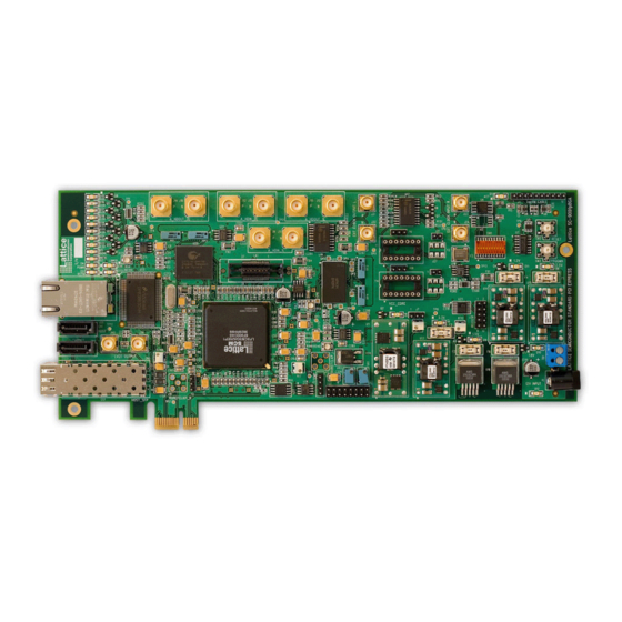
- Page 2 Evaluation Board User’s Guide Introduction This user’s guide describes the LatticeSC PCI Express x1 Evaluation Board featuring the LatticeSC LFSCM3GA25 device in a 900 fpBGA package. The stand-alone evaluation PCB provides a functional platform for development and rapid prototyping of applications that require high-speed SERDES interfaces to PCI Express protocols.
-
Page 3: Additional Resources
Figure 2 shows the functional partitioning of the board. Figure 2. LatticeSC PCI Express x1 Evaluation Board Block Diagram Backpanel Slot 12V Edge Fingers... -
Page 4: Applying Power To The Board
Applying Power to the Board The LatticeSC PCI Express x1 Evaluation Board is ready to power on. The board can be supplied with power from an AC wall-type transformer power supply shipped with the board or it can be supplied from a bench top supply via terminal screw connections. -
Page 5: Programming/Fpga Configuration
LatticeSC PCI Express x1 Lattice Semiconductor Evaluation Board User’s Guide Table 1. Board Power Supply Fuses (see Appendix A, Figure 6) 1.0V/1.2V Core Fuse 1.5V Fuse 3.3V Fuse 1.2V Fuse 2.5V Fuse 1.8V Fuse Table 2. Board Power Supply Indicators (see Appendix A, Figure 6) 2.5V Source Good Indicator... - Page 6 1. Connect the ispDOWNLOAD cable to the appropriate header. J3 is used for the 1x10 cable. Connections to J3 use only pins[1-3][6-8]. 2. Connect the LatticeSC PCI Express x1 evaluation board to the appropriate power sources and power up board.
-
Page 7: Configuration Status Indicators
LatticeSC PCI Express x1 Lattice Semiconductor Evaluation Board User’s Guide 4. Press the SCAN button located in the toolbar. The LatticeSC device is automatically detected. 5. Double-click the device to open the device information dialog. In the device information dialog, click the Browse button located under Data File . -
Page 8: Fpga Clock Management
LatticeSC PCI Express x1 Lattice Semiconductor Evaluation Board User’s Guide • D5 (GREEN) is illuminated: This indicates the successful completion of configuration by releasing the open col- lector DONE output pin. • D1 (GREEN) will flash indicating TDI activity. • D4 (RED) illuminated: This indicates that PROGRAMN is low. - Page 9 LatticeSC PCI Express x1 Lattice Semiconductor Evaluation Board User’s Guide Table 5. Clock Source Selection (see Appendix A, Figures 5 and 10) BGA-A19 BGA-A20 Clock Source Clock Source Oscillator Oscillator Oscillator Oscillator Oscillator Pin is low when open/float. When using FPGA control, 3.3V VCCIO must be used in bank 1. Refer to Bank1 VCCIO section of this document.
-
Page 10: Serdes Channels
LatticeSC PCI Express x1 Lattice Semiconductor Evaluation Board User’s Guide SERDES Channels SMA Connections (see Appendix A, Figure 5) DC coupled top-mounted SMA connectors connect to the two SERDES TX and RX channels. These pins are directly coupled to the designated SMA connector creating a path for both input and output differential data. -
Page 11: Fpga Test Pins
LatticeSC PCI Express x1 Lattice Semiconductor Evaluation Board User’s Guide Table 12. SERDES to SATA Connections 900-Ball 900-Ball CN1 Pin SERDES Pin fpBGA CN2 Pin SERDES Pin fpBGA A_HDOUTP1_R A_HDINP2_R A_HDOUTN1_R A_HDINN2_R A_HDINP1_R A_HDOUTP2_R A_HDINN1_R A_HDOUTN2_R SERDES PCI Express Channels (see Appendix A, Figure 8) This board is equipped to communicate directly as an add-on card to a PCI Express host. -
Page 12: Test Sma Connections
LatticeSC PCI Express x1 Lattice Semiconductor Evaluation Board User’s Guide Test SMA Connections General-purpose FPGA pins are available via SMA test connections. These connections are designed to permit evaluations of several types of FPGA I/O buffers. The use of several termination schemes permits easy interfaces for the type of buffer. -
Page 13: Lcd Interface
LatticeSC PCI Express x1 Lattice Semiconductor Evaluation Board User’s Guide Table 17. Logic Analyzer Connections (Continued) MICTOR Pin Signal 900-Ball fpBGA MICTOR Pin Signal 900-Ball fpBGA LA_10 LA_26 AJ13 LA_11 LA_27 AD15 LA_12 AF14 LA_28 AE15 LA_13 AF15 LA_29 AK12... - Page 14 LatticeSC PCI Express x1 Lattice Semiconductor Evaluation Board User’s Guide design to be included in the FPGA. The board includes two status LEDs to indicate Base 10 or Base 100 link. LED(D13) is a green LED which will light to indicate a Base100 link and LED(D14) indicates an established Base 10 link.
- Page 15 LatticeSC PCI Express x1 Lattice Semiconductor Evaluation Board User’s Guide Table 21. QDR2 Memory Interface Pinouts (Continued) NetName FPGA Ball NetName FPGA Ball NetName FPGA Ball AH28 AK18 AJ28 AK19 AE22 AH17 A_10 Q_10 AK29 D_10 AH18 A_11 Q_11 AK28...
-
Page 16: Ordering Information
Added important information for proper connection of ispDOWNLOAD (Programming) Cables. © 2007 Lattice Semiconductor Corp. All Lattice trademarks, registered trademarks, patents, and disclaimers are as listed at www.latticesemi.com/legal. All other brand or product names are trademarks or registered trademarks of... -
Page 17: Appendix A. Schematic
LatticeSC PCI Express x1 Lattice Semiconductor Evaluation Board User’s Guide Appendix A. Schematic Figure 4. Cover Page... - Page 18 LatticeSC PCI Express x1 Lattice Semiconductor Evaluation Board User’s Guide Figure 5. Configuration/Top Bank...
- Page 19 LatticeSC PCI Express x1 Lattice Semiconductor Evaluation Board User’s Guide Figure 6. Power Supplies...
- Page 20 LatticeSC PCI Express x1 Lattice Semiconductor Evaluation Board User’s Guide Figure 7. DC/DC Conversion...
- Page 21 LatticeSC PCI Express x1 Lattice Semiconductor Evaluation Board User’s Guide Figure 8. SERDES...
- Page 22 LatticeSC PCI Express x1 Lattice Semiconductor Evaluation Board User’s Guide Figure 9. SERDES Power Supplies...
- Page 23 LatticeSC PCI Express x1 Lattice Semiconductor Evaluation Board User’s Guide Figure 10. Clocks...
- Page 24 LatticeSC PCI Express x1 Lattice Semiconductor Evaluation Board User’s Guide Figure 11. Clocks (Cont.)
- Page 25 LatticeSC PCI Express x1 Lattice Semiconductor Evaluation Board User’s Guide Figure 12. QDR2 SRAM QDR_D[0..17]...
- Page 26 LatticeSC PCI Express x1 Lattice Semiconductor Evaluation Board User’s Guide Figure 13. 10/100/1000 PHY...
- Page 27 LatticeSC PCI Express x1 Lattice Semiconductor Evaluation Board User’s Guide Figure 14. RLDRAM...
- Page 28 LatticeSC PCI Express x1 Lattice Semiconductor Evaluation Board User’s Guide Figure 15. FPGA Banks QDR_D[0..17] QDR_Q[0..17]...
- Page 29 LatticeSC PCI Express x1 Lattice Semiconductor Evaluation Board User’s Guide Figure 16. I C RS232 Test...
- Page 30 LatticeSC PCI Express x1 Lattice Semiconductor Evaluation Board User’s Guide Figure 17. VSS Decoupling...
Need help?
Do you have a question about the LatticeSC PCI Express x1 and is the answer not in the manual?
Questions and answers