Lattice Semiconductor LatticeECP3 User Manual
Serial protocol board revision e
Hide thumbs
Also See for LatticeECP3:
- User manual (35 pages) ,
- User manual (34 pages) ,
- User manual (33 pages)

Related Manuals for Lattice Semiconductor LatticeECP3


Summary of Contents for Lattice Semiconductor LatticeECP3
- Page 1 LatticeECP3™ Serial Protocol Board – Revision E User’s Guide November 2012 Revision: EB49_01.4...
-
Page 2: Board Features
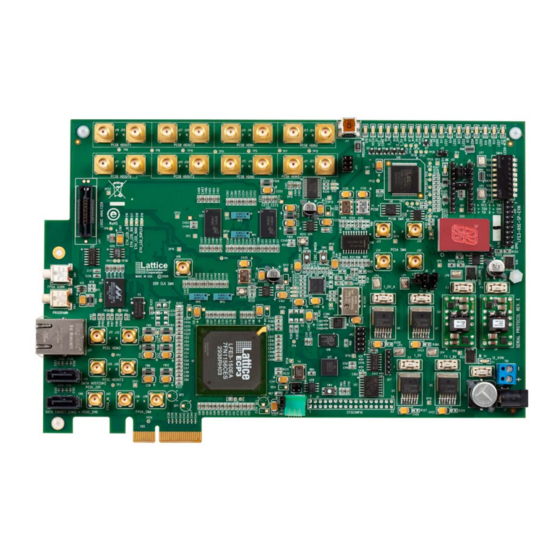
User’s Guide Introduction The LatticeECP3 Serial Protocol Board (referred to in this document as “SPB”) allows designers to investigate and experiment with the features of the LatticeECP3 high-speed SERDES transceivers. The SPB is available for full and detailed characterization of the high speed I/O channels and includes interfaces for some of the latest protocol interconnections. - Page 3 LatticeECP3 Serial Protocol Board – Revision E User’s Guide – x4 is non-compliant but will demonstrate x4 functionality with an open-frame motherboard • Allow control of SERDES PCS registers using the Serial Client Interface (ORCAstra) • Serial ATA interfaces for host and target configurations •...
-
Page 4: Latticeecp3 Device
Applying Power to the Board The LatticeECP3 Serial Protocol Board is ready to power on. The board can be supplied with power from an AC wall-type transformer power supply shipped with the board. Or, it can be supplied from an benchtop supply via ter- minal screw connections. -
Page 5: Programming/Fpga Configuration
3_3V, +3.3V, 2A Programming/FPGA Configuration (see Appendix A, Figure 23) A programming header is provided on the evaluation board, providing access to the LatticeECP3 JTAG port. ® Note: An ispDOWNLOAD™ Cable is included with each ispLEVER -Base or ispLEVER-Advanced design tool shipment. -
Page 6: Programming The Daisy Chain
LatticeECP3 Serial Protocol Board – Revision E User’s Guide Table 4. Standard ispVM Programming Cable Configuration Description Pin 1 Pin 2 Pin 3 Pin 4 PROGRAMN Pin 5 Enable used for alternate programming of the ispPAC-POWR1220AT8 device Pin 6 Pin 7... -
Page 7: Download Procedure
• ispDOWNLOAD Cable (pDS4102-DL2A, HW7265-DL3A, HW-USB-1A, etc.) JTAG Download The LatticeECP3 device can be configured easily via its JTAG port. The device is SRAM-based; it must remain powered on to retain its configuration when programmed in this fashion. 1. Connect the LatticeECP3 Serial Protocol Board to the appropriate power sources and power up board. - Page 8 6. Add the data file from the Browse dialog and select OK when complete. 7. To program only the LatticeECP3-95, place the LCMXO1200C and the ispPAC-POWR1220AT8 devices into BYPASS and the LFE3-95 into Erase, Program, Verify mode, as shown below.
-
Page 9: Programming The Power Manager Device
LatticeECP3 Serial Protocol Board – Revision E User’s Guide Figure 8. Successful Programming Session 8. Click the green GO button. This will begin the download process into the device. Upon successful download, the device will be operational. Programming the Power Manager Device The J12 header can be used to isolate and program the ispPAC-POWR1220AT8 Power Manager device. -
Page 10: Configuration Status Indicators
LatticeECP3 Serial Protocol Board – Revision E User’s Guide Figure 9. Setup for ISPEN Usage Figure 10. Programming of ispPAC-POWR1220AT8 Power Manager Device Note: The ispEN connection must be disconnected for complete programming of the other devices on the SPB. - Page 11 LatticeECP3 Serial Protocol Board – Revision E User’s Guide • D10 (red) illuminated, this indicates that PROGRAMN is low. • D9 (red) illuminated, this indicates that GSRN is low. PROGRAMN and GSRN (see Appendix A, Figure 23) • These push-button switches assert/de-assert the logic levels on the PROGRAMN (SW3) and GSRN (SW1).
- Page 12 LatticeECP3 Serial Protocol Board – Revision E User’s Guide Figure 11. Device Information Dialog Screen 7. The SPI Serial Flash Device dialog box will open. In this box select SPI Flash Erase, Program, Verify in the Operation pull-down menu. 8. Select SPI Serial Flash in the Device Family pull-down menu, STMicro under the Vendor pull-down menu, SPI-M2564 under the Device pull-down menu, and 16-lead SOIC under the Package submenu.
- Page 13 LatticeECP3 Serial Protocol Board – Revision E User’s Guide Figure 13. Sample SPI Serial Flash Device Dialog Box 9. Click OK in the SPI Flash Device Dialog box. Then click OK in Select Device dialog box. You will then return to the main configuration screen.
-
Page 14: On-Board Parallel Spi Flash Memory
LatticeECP3 Serial Protocol Board – Revision E User’s Guide Figure 15. Programming Main Window Figure 16. SPI Serial Flash Programming Status Window Figure 17. Successful SPI Serial Flash Programming Session On-Board Parallel SPI Flash Memory (see Appendix A, Figure 25) •... -
Page 15: On-Board Clock Capabilities
LatticeECP3 Serial Protocol Board – Revision E User’s Guide allel Flash devices. Application note AN8077, Parallel Flash Programming and FPGA Configuration, addresses the use of the parallel Flash implementation. On-Board Clock Capabilities Dedicated SERDES Reference Clock Inputs (see Appendix A, Figure 26) •... - Page 16 LatticeECP3 Serial Protocol Board – Revision E User’s Guide DC coupled top-mounted SMA connectors connect to the one quad or four SERDES Tx and Rx channels. These pins are directly coupled to the designated SMA connector creating a path for both input and output differential data.
- Page 17 LatticeECP3 Serial Protocol Board – Revision E User’s Guide Table 10. x4 PCI Express Connections PCI Express CML Pin Name FPGA Pin Express Edge Description PCSA_HDOUTP_3 AP18 PERp0 Integrated end point block transmit pair PCSA_HDOUTN_3 AN18 PERn0 PCSA_HDINP_3 AL18 PETp0...
-
Page 18: Fpga Test Pins
LatticeECP3 Serial Protocol Board – Revision E User’s Guide loop bandwidth, jitter can be cleaned. For the CDC7005, a low loop (sub 10 Hz) bandwidth can be selected easily. The CDC7005 itself adds a low noise to its outputs. For jitter cleaning operation, the noise performance of VCXO is critical. -
Page 19: General-Purpose Leds
LatticeECP3 Serial Protocol Board – Revision E User’s Guide Table 15. FPGA Test Pins (See Appendix A, Figure 33) 1156 fpBGA SW14 Ball Number Switch Position AA29 General-Purpose LEDs (see Appendix A, Figure 31) The LEDs on the evaluation board are connected to general-purpose FPGA I/O. The purpose of these LEDs is to provide status for user designs. - Page 20 LatticeECP3 Serial Protocol Board – Revision E User’s Guide 17-Segment LED Display (see Appendix A, Figure 33, D20) General-purpose FPGA pins are connected to a 17-segment display according to Table 18. These pins can be driven low to illuminate the display segments.
- Page 21 PCB Amber (D19) DUPLEX The Marvell 88E1111 device communicates via a MAC interface to the LatticeECP3 device via GMII, SGMII, and a standard 10-bit interface. The evaluation board includes the means to setup the required hardware configuration for the PHY to operate in all the supported modes. Hardware configuration options such as PHY address, PHY operat- ing mode, auto-negotiation, and physical connection type must be set up using the configuration switches SW7 to SW13 on the back side of the board.
- Page 22 LatticeECP3 Serial Protocol Board – Revision E User’s Guide Table 21. PHY Hardware Configuration Switch Control (see Appendix A, Figure 29) Switch 88E1111 LED Position Output Bit[2:0] 88E1111 Hardware Register Map VDDO 88E1111 Pin Bit[2] Bit[1] Bit[0] LED_10 CONFIG0 PHYADDR[2] PHYADDR[1]...
- Page 23 LatticeECP3 Serial Protocol Board – Revision E User’s Guide Table 23. Marvel Transceiver Configuration Defaults PHY Config Position Encoded Encoded DIP Switch Output Pin Value Description CONFIG0 LED TX PHY ADDR[2:0] = 001 CONFIG1 ENABLE PAUSE, PHY ADDR[4:3] = 00...
-
Page 24: Crossover Pld Device
LatticeECP3 Serial Protocol Board – Revision E User’s Guide Table 25. 88E1111 Control and Status Interconnections to FPGA (see Appendix A, Figure 33) 1156 fpBGA Control/Status 88E1111 Pin Ball Number MDIO RESETn INTn FREQ_SEL CLK25 Crossover PLD Device (see Appendix A, Figure 25, U17) The board includes a Lattice LCMXO-1200C Crossover PLD which is used in conjunction with the parallel Flash device for loading the configuration memory of the FPGA. - Page 25 LatticeECP3 Serial Protocol Board – Revision E User’s Guide Table 27. DDR2 Memory Interface Connections DDR2 Memory Signal FPGA Pin DDR2 Memory Signal FPGA Pin U32-B9 DQ31 U25,U32-M8 U32-B1 DQ30 U25,U32-M3 U32-D9 DQ29 U25,U32-M7 U32-D1 DQ28 U25,U32-N2 U32-D3 DQ27 U25,U32-N8...
-
Page 26: Ordering Information
01.4 SERDES SMA Test Connectors table – Updated connector numbers. © 2012 Lattice Semiconductor Corp. All Lattice trademarks, registered trademarks, patents, and disclaimers are as listed at www.latticesemi.com/legal. All other brand or product names are trademarks or registered trademarks of... -
Page 27: Appendix A. Schematic
LatticeECP3 Serial Protocol Board – Revision E User’s Guide Appendix A. Schematic Figure 20. Cover Page... - Page 28 LatticeECP3 Serial Protocol Board – Revision E User’s Guide Figure 21. Power Generation...
- Page 29 LatticeECP3 Serial Protocol Board – Revision E User’s Guide Figure 22. Power Management...
- Page 30 LatticeECP3 Serial Protocol Board – Revision E User’s Guide Figure 23. Power Supplies...
- Page 31 LatticeECP3 Serial Protocol Board – Revision E User’s Guide Figure 24. Programming FPGA_D[8..15] PROGRAMN DONE INITN...
- Page 32 LatticeECP3 Serial Protocol Board – Revision E User’s Guide Figure 25. Parallel FPGA Loader...
- Page 33 LatticeECP3 Serial Protocol Board – Revision E User’s Guide Figure 26. SERDES...
- Page 34 LatticeECP3 Serial Protocol Board – Revision E User’s Guide Figure 27. Clock Cleaner...
- Page 35 LatticeECP3 Serial Protocol Board – Revision E User’s Guide Figure 28. 1000BASE-T PHY/RJ45...
- Page 36 LatticeECP3 Serial Protocol Board – Revision E User’s Guide Figure 29. PHY Configuration...
- Page 37 LatticeECP3 Serial Protocol Board – Revision E User’s Guide Figure 30. Memory Controllers...
- Page 38 LatticeECP3 Serial Protocol Board – Revision E User’s Guide Figure 31. DDR2 Memory DDR2_A[0:12]...
- Page 39 LatticeECP3 Serial Protocol Board – Revision E User’s Guide Figure 32. FPGA Pins...
- Page 40 LatticeECP3 Serial Protocol Board – Revision E User’s Guide Figure 33. FPGA Test...
- Page 41 LatticeECP3 Serial Protocol Board – Revision E User’s Guide Figure 34. Miscellaneous...
- Page 42 LatticeECP3 Serial Protocol Board – Revision E User’s Guide Figure 35. VSS/Decoupling...
-
Page 43: Appendix B. Bill Of Materials
LatticeECP3 Serial Protocol Board – Revision E User’s Guide Appendix B. Bill of Materials Table 28. Bill of Materials Item Quantity Reference Part Manufacturer Part Number Description CN1, CN2 SATA Molex 67800-1005/ CONN HEADER 7POS VERT DK#WM19023-ND SMD 15GOLD PCI Express x4 PCB Edge finger Edge Finger Conn. - Page 44 LatticeECP3 Serial Protocol Board – Revision E User’s Guide Table 28. Bill of Materials (Continued) Item Quantity Reference Part Manufacturer Part Number Description C346, C347, C348, C349, C350, C351, 1000PF-0402SMT Panasonic ECJ-0EB1E102K CAP 1000PF 25V CERAMIC C352, C353, C354, C355, C356, C357,...
- Page 45 LatticeECP3 Serial Protocol Board – Revision E User’s Guide Table 28. Bill of Materials (Continued) Item Quantity Reference Part Manufacturer Part Number Description R3, R4, R24, R25, R80, R207, R209, R211, 0R-0603SMT Panasonic ERJ-3GEY0R00V RES ZERO OHM 1/10W 5% R215, R217, R222, R227, R236, R237,...
- Page 46 LatticeECP3 Serial Protocol Board – Revision E User’s Guide Table 28. Bill of Materials (Continued) Item Quantity Reference Part Manufacturer Part Number Description Alt: CRCW040282R0FKED R146 OPEN-0402SMT R150, R151, R154 750R-0402SMT Panasonic ERJ-2RKF7500X RES 750 OHM 1/16W 1% 0402 SMD...
- Page 47 LatticeECP3 Serial Protocol Board – Revision E User’s Guide Table 28. Bill of Materials (Continued) Item Quantity Reference Part Manufacturer Part Number Description LT1963-ADJ Linear Tech LT1963ES8 IC REG LDO ADJ 1.5A LN 8SOIC 88e1111 Marvell 88e1111-Bx-BAB-C000( single-port Gigabit Ether-...
- Page 48 LatticeECP3 Serial Protocol Board – Revision E User’s Guide Table 28. Bill of Materials (Continued) Item Quantity Reference Part Manufacturer Part Number Description R353, R354, R355, R356 1K-0603SMT Panasonic ERJ-3EKF1001V RES 1.00K OHM 1/16W 1% 0603 SMD R338, R339 62R-0603SMT...
- Page 49 LatticeECP3 Serial Protocol Board – Revision E User’s Guide Table 28. Bill of Materials (Continued) Item Quantity Reference Part Manufacturer Part Number Description RES ZERO OHM 1/10W 5% R402 0R-0603SMT Panasonic ERJ-3GEY0R00V 0603 SMD C469, C470 330UF-DL3POSCAP Sanyo 6TPE330MIL 6.3V ,D3L. POSCAP...
- Page 50 Mouser Electronics Authorized Distributor Click to View Pricing, Inventory, Delivery & Lifecycle Information: Lattice LFE3-95EA-SP-EVN...
Need help?
Do you have a question about the LatticeECP3 and is the answer not in the manual?
Questions and answers