
Subscribe to Our Youtube Channel
Related Manuals for Lattice Semiconductor LatticeEC


Summary of Contents for Lattice Semiconductor LatticeEC
- Page 1 LatticeEC™ Advanced Evaluation Board – Revision C User’s Guide April 2007 EB11_02.4...
-
Page 2: Electrical, Mechanical And Environmental Specifications
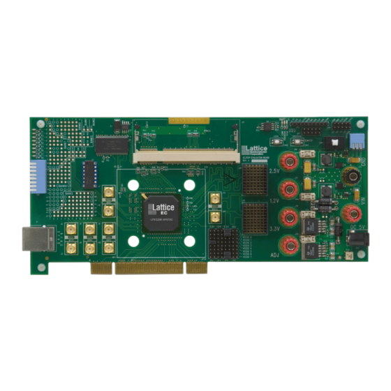
The LatticeEC Advanced Evaluation Board provides a convenient platform to evaluate, test, and debug designs with the support of LatticeEC advanced interface capabilities. The board provides easy access to PCI, DDR SDRAM, FCDRAM and SPI4.2 interfaces. The information in this document pertains only to boards marked as ‘Rev C’. -
Page 3: Additional Resources
A jumper installed on JP7 provides a connection between the configuration clock (CCLK) and a general-purpose I/O. JP7 must be installed to program the SPI Serial Flash through the LatticeEC device using JTAG; the jumper must be removed to configure the LatticeEC device from SPI Flash (see the section in this document entitled SPI Flash Download via JTAG). -
Page 4: Power Setup
LatticeEC Advanced Evaluation Board – Lattice Semiconductor Revision C User’s Guide Power Setup For stand-alone board operation (i.e. outside of a PCI backplane), the evaluation board may be supplied with a sin- gle 5V DC power supply. On-board regulators will provide the supply voltages necessary for each component. The... - Page 5 CCIO sysCONFIG port when interfacing to SPI3 Flash memory devices. The following tables detail the various standards supported by the LatticeEC FPGA Input/Output (sysIO) struc- tures. More information can be found in Lattice technical note number TN1056, LatticeECP/EC sysIO Usage Guide , available on the Lattice web site at www.latticesemi.com.
- Page 6 LatticeEC Advanced Evaluation Board – Lattice Semiconductor Revision C User’s Guide Table 8. sysIO Standards Supported per Bank Top Side Right Side Bottom Side Left Side Description Banks 0-1 Banks 2-3 Banks 4-5 Banks 6-7 Types of I/O Buffers Single-ended...
- Page 7 Lattice Semiconductor Revision C User’s Guide The LatticeEC Evaluation Board is designed to interface directly to PCI 2.2 compatible systems using the PCI edge connector. All necessary signals required for 32-bit PCI operation are provided to the connector, as shown in Tables 9 and 10.
- Page 8 LatticeEC Advanced Evaluation Board – Lattice Semiconductor Revision C User’s Guide Table 10. PCI Connections – Component Side Description LatticeEC Pin sysIO Bank PCI_INTB_N AA12 PCI_INTD_N AF13 PCI_PRSNT1_N AE13 PCI_PRSNT2_N AD13 PCI_CLK PCI_REQ_N AA13 PCI_AD31 AE14 PCI_AD29 AC14 PCI_AD27 AA14...
- Page 9 LatticeEC Advanced Evaluation Board – Lattice Semiconductor Revision C User’s Guide SPI 4.2 Provided for SPI 4.2 interfaces are two 6x10 backplane connectors. Connector J15 includes necessary data pairs and control signals for transmit data, while J14 has been configured for receive data. Standard 100-ohm differential termination is provided for all applicable receive signal pairs.
- Page 10 LatticeEC Advanced Evaluation Board – Lattice Semiconductor Revision C User’s Guide Table 12. SPI4.2 Receive Connections Description LatticeEC Pin sysIO Bank Notes SPI4_RDAT_P14 100-ohm LVDS termination SPI4_RDAT_P12 100-ohm LVDS termination SPI4_RDAT_P10 100-ohm LVDS termination SPI4_RDAT_P8 100-ohm LVDS termination SPI4_RDAT_P6 100-ohm LVDS termination...
-
Page 11: Ddr Sdram
LatticeEC Advanced Evaluation Board – Lattice Semiconductor Revision C User’s Guide DDR SDRAM The included 200-pin SODIMM socket provides a built-in 16-bit interface to standard 2.5V DDR SDRAM memory modules. The required V and V voltages, as well as termination of each signal to V are provided. - Page 12 LatticeEC Advanced Evaluation Board – Lattice Semiconductor Revision C User’s Guide Table 13. DDR Interface to SODIMM Socket (Continued) Description LatticeEC Pin sysIO Bank SODIMM_WE_N SODIMM_CAS_N SODIMM_S0_N SODIMM_S1_N FCRAM Included with the evaluation board is a 256Mb (8Mb x 4 x 8-bit) FCRAM device. All necessary voltages and signal terminations are supplied.
- Page 13 SW1 are wired to 2.5V, but any I/O voltage up to 3.3V may be used. A switch in the down position produces a low (0), the up position produces a high (1). Table 16 shows the connections to the LatticeEC I/O pins.
- Page 14 SW4, when in position 1 (up), connects the download cable to the SPI Flash so that the user can program the Flash. When SW4 is in position 2 (down) the SPI Flash is connected to the LatticeEC FPGA; pressing and releas- ing SW3 (assuming the configuration switch, SW5, is properly set) will configure the FPGA.
-
Page 15: Download Procedures
• ispDOWNLOAD Cable (pDS4102-DL2A, HW7265-DL3A, HW-USB-1A, etc.) JTAG Download The LatticeEC device can be configured easily via its JTAG port. The device is SRAM-based, so the it must remain powered on to retain its configuration when programmed in this fashion. - Page 16 2. Connect the LatticeEC Evaluation Board to an external 5V supply. 3. Start the ispVM System software. 4. Press the ‘SCAN’ button located in the toolbar. The LatticeEC device should be automatically detected. The resulting screen should be similar to Figure 2.
- Page 17 1. Set switch SW5 to “000”. This enables SPI3 mode by setting the CFG pins of the LatticeEC device. 2. Set switch SW4 to position 1 (up) to enable the SPI3 connections from the programming headers directly to the SPI3 device.
- Page 18 LatticeEC Advanced Evaluation Board – Lattice Semiconductor Revision C User’s Guide 7. Insert a new device into the chain (Edit->Add Device). 8. In the resulting Device Information dialog, shown in Figure 4, press the ‘Select’ button. Figure 4. Device Selector Dialog 9.
- Page 19 LatticeEC Advanced Evaluation Board – Lattice Semiconductor Revision C User’s Guide Figure 6. SPI Device Selection 12. Choose the ‘Configuration Data Setup’ page, as shown in Figure 14. Figure 7. Configuration Data Setup Page 13. Click the ‘Browse’ button near the top of the window. Browse to the desired bitstream (.bit) file, created by the ®...
- Page 20 Note: When using a 1x8 download cable, connect to the 1x10 header by justifying the alignment to pin 1 (Vcc). 5. Start the ispVM System software. 6. Press the ‘SCAN’ button located in the toolbar. The LatticeEC device should be automatically detected. The resulting screen should appear similar to Figure 8.
- Page 21 Figure 9. Setting the Device Access Options Note: Selection of the ‘Advanced SPI Flash Programming’ option allows the user to specify a data file other than the ispVM System default. This is necessary for the LatticeEC Advanced Evaluation Board. Figure 10. SPI Flash Programmer...
- Page 22 9. Click the ‘Browse’ button to select an alternate Application Specific Data File. Choose the ‘ec20_adv_revc_spi_loader.bit’ file. Note: This file is available in the Design Files section of the LatticeEC Advanced Evaluation Board on the Lattice web site (www.latticesemi.com). 10. Select the ‘Configuration Data Setup’ page, as shown in Figure 12.
-
Page 23: Ordering Information
Added important information for proper connection of ispDOWNLOAD (Programming) Cables. © 2007 Lattice Semiconductor Corp. All Lattice trademarks, registered trademarks, patents, and disclaimers are as listed at www.latticesemi.com/legal. All other brand or product names are trademarks or registered trademarks of... -
Page 24: Appendix A. Schematics
LatticeEC Advanced Evaluation Board – Lattice Semiconductor Revision C User’s Guide Appendix A. Schematics Figure 14. Evaluation Board Block Diagram... - Page 25 LatticeEC Advanced Evaluation Board – Lattice Semiconductor Revision C User’s Guide Figure 15. 32-Bit PCI Interface...
- Page 26 LatticeEC Advanced Evaluation Board – Lattice Semiconductor Revision C User’s Guide Figure 16. DDR SDRAM and FCRAM...
- Page 27 LatticeEC Advanced Evaluation Board – Lattice Semiconductor Revision C User’s Guide Figure 17. SPI 4.2...
- Page 28 LatticeEC Advanced Evaluation Board – Lattice Semiconductor Revision C User’s Guide Figure 18. JTAG and FPGA Programming...
- Page 29 LatticeEC Advanced Evaluation Board – Lattice Semiconductor Revision C User’s Guide Figure 19. Prototyping Support...
- Page 30 LatticeEC Advanced Evaluation Board – Lattice Semiconductor Revision C User’s Guide Figure 20. Power...
- Page 31 LatticeEC Advanced Evaluation Board – Lattice Semiconductor Revision C User’s Guide Figure 21. Mechanical Drawing...
- Page 32 Mouser Electronics Authorized Distributor Click to View Pricing, Inventory, Delivery & Lifecycle Information: Lattice LFECP20E-H-EV...
Need help?
Do you have a question about the LatticeEC and is the answer not in the manual?
Questions and answers