Table of Contents
Advertisement
Quick Links
Advertisement
Table of Contents

Related Manuals for Lattice Semiconductor L-ASC10


Summary of Contents for Lattice Semiconductor L-ASC10
- Page 1 ASC Breakout Board User Guide EB92 Version 1.0, July 2015...
- Page 2 Thank you for choosing the Lattice Semiconductor ASC Breakout Board. This guide describes how to begin using the L-ASC10 (ASC) Breakout Board, an easy-to-use platform for evaluat- ing and designing with the ASC programmable hardware management expander. This board is designed for use with a Lattice FPGA evaluation board such as the Platform Manager 2 evaluation board.
-
Page 3: Asc Breakout Board Photos
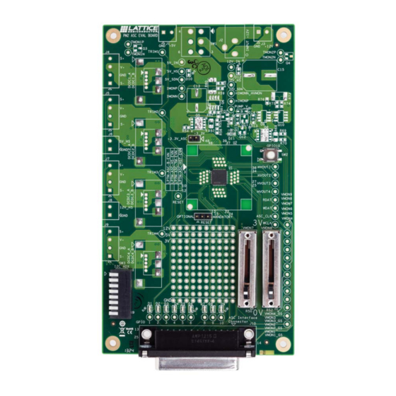
ASC Breakout Board ASC Breakout Board Photos Photographs of the top and bottom of ASC Breakout Board are shown in Figure 1 and Figure 2 below. These pho- tographs show the board with the Hot Swap and Trim circuits populated (which are not populated in the released version of the breakout board). - Page 4 ASC Breakout Board Figure 2. ASC Breakout Board - Bottom View...
-
Page 5: Board Hardware Features
Plane Management) Expander designed to be used with Lattice FPGAs to implement the Hardware Management Control function in a circuit board. The L-ASC10 (referred to as ASC) enables seamless scaling of power supply voltage and current monitoring, temperature monitoring, sequence and margin control channels. The ASC includes dedicated interfaces supporting the exchange of monitor signal status and output control signals with these central- ized hardware management controllers. -
Page 6: Voltage Monitoring
ASC Breakout Board Figure 3. ASC Block Diagram MOSFET & Digital I/O Drive Output Control Block Interface (ASC-I/F) Non - Volatile Fault Log Interface Trim & Margin Control Voltage Monitoring There are 10 VMON inputs to the analog section of the device (including the HIMONN_HVMON pin). These are routed to slide potentiometers, board power supplies (not populated), and the on-board Hot Swap circuits (not pop- ulated). - Page 7 ASC Breakout Board Schematic Component / Signals Ref. Des. Description Sheet Components Not Populated on Breakout Board Ω Series Resistors , R32 resistor allows the user to safely drive VMON1 and VMON2 test points with an off-board voltage source. (Only needed when DCDC1 and DCDC2 are populated.) Ω ...
-
Page 8: Temperature Monitoring
ASC Breakout Board The two potentiometers (R50 and R52) are tied to VMON7 and VMON8 these can be used to simulate a fault or trip a comparator (see Figure 4). The slide potentiometers provide a voltage in the range of 0 V to 3.3 V depending on their position. -
Page 9: Led Outputs
Signals TEMP_SENSE1P / 2, 5 Input from temperature sensor to TMON1 (tempera- TEMP_SENSE1N ture monitor input) of L-ASC10 TEMP_SENSE2P / 2, 5 Input from temperature sensor to TMON2 (tempera- TEMP_SENSE2N ture monitor input) of L-ASC10 LED Outputs The ASC Breakout Board has 9 LEDs tied to the ASC open-drain outputs. -
Page 10: Reset Configuration Jumper
ASC Breakout Board Figure 8. Push-Button Circuit LED10 GPIO10 C Address Selection DIP Switch The ASC Breakout Board provides an 8-position DIP switch for I C address selection of the ASC device. The switch combines with a set of on-board resistors (R9 – R15) to connect to the I2C_ADDR pin of the device (shown in Figure 9, taken from Sheet 2 of the schematic). -
Page 11: Asc Interface Connector
ASC Breakout Board ASC Interface Connector The ASC Interface Connector (shown in Figure 11 from Schematic Sheet 2) is used to connect the ASC Breakout Board to the main FPGA Board. The connector has been designed to pair with other available Lattice Evaluation Boards, including the Platform Manager 2 Evaluation Board (see the related literature section for more details). - Page 12 ASC Breakout Board Pin # Signal Name Description +3.3V ASC Supply Voltage. Provided by FPGA board or 12 V power supply (power supply not populated on Breakout Board). +11.3V Voltage rail generated from diode OR of +12V_SW and +5_SW input supplies.
-
Page 13: Closed Loop Trimming (Not Populated)
ASC Breakout Board Closed Loop Trimming (Not Populated) The ASC provides four Closed Loop Trim (CLT) cells which are used to accurately trim and margin power supplies. The ASC Breakout Board provides four DC-DC converter and trimming circuit footprints on the breakout board. Table 4 lists the components and signal associated with CLT operation on the ASC Breakout Board. - Page 14 ASC Breakout Board Schematic- Component / Signals Ref. Des. Description Sheet LED5 2, 4 DCDC4 control signal from GPIO5. Safe state is low. OUT_DCDC1 2, 3 DCDC1 Output connected to VMON1 via R23. OUT_DCDC2 2, 3 DCDC2 Output connected to VMON2 via R32. OUT_DCDC3 2, 4 DCDC3 Output connected to VMON3 via R40.
- Page 15 ASC Breakout Board source to be applied to the VMON test point directly. If the voltage source is fairly weak, the VMON series resistor can be removed. Each of the DC-DC supplies has a load resistor connected to the output. The load resistor is not required in cus- tomer designs as the supply is typically connected to a real load.
-
Page 16: Board Power Supplies (Not Populated)
ASC Breakout Board Table 6 shows a summary of the input voltage, output voltage, and control signal behavior for each of the four DC- DC converters. The +12V_HS and +5V_HS rails which are used to power the DC-DC converters can be provided by either the Hot Swap circuits or the ASC Interface Board connector. - Page 17 ASC Breakout Board Figure 13. Board Power Supply Circuit +11.3V +12V +11.3V Sheet [2] PWR JACK NSR0530P2T5G +12V_SW Sheet [7,10] TRANZORB 2 Position Terminal Block SW DPDT +3.3V +5V_SW Sheet [2,6,10] +3.3V Sheet [2,3,4,5,6,7,8,10] 2 Position Terminal Block Populate jumper to provide DCDC5 3.3V power from ASC Eval Board +11.3V...
- Page 18 ASC Breakout Board Schematic Component / Signals Ref. Des. Description Sheet MOSFET with Sense Output N-Channel MOSFET supply-side Hot Swap switch supplies power to +5V_HS and load capacitor C13. Sense output pro- vides proportional current to drain current. Ω Gate Drive Resistor 2.2 k resistor, located close to MOSFET Q5, limits parasitic oscillations at the gate of Q5.
- Page 19 ASC Breakout Board Figure 14. 5 V Hot Swap Circuit MOSFET w/ Sense (Option B) Population Options: Standard MOSFET (Option A): Q6, C22, R61, BUK7C06-40AITE R60, R58, R59 MOSFET w/ Sense (Option B): sense X 600 Q5, R57, R55, C23, R54, R56 3.30 100nF TP12...
- Page 20 ASC Breakout Board Figure 15. 5 V Hot Swap - Load-Based, Standard MOSFET Shared Connection with MOSFET with Sense Hot Swap TP12 +5V_HS 5V_HS IRF7832 0.005 VMON6 2W, 1% From 5V_SW Supply Voltage 3.3k 100nF To ASC IMON 1P 680uF Current Monitor 4.7k SM_LED_0603...
- Page 21 ASC Breakout Board Figure 16. 5 V Hot Swap - Supply Based, SENSEFET Note: Components not populated MOSFET w/ Sense (Option B) Population Options: on breakout board Standard MOSFET (Option A): Q6, C22, R61, BUK7C06-40AITE R60, R58, R59 MOSFET w/ Sense (Option B): sense X 600 Q5, R57, R55, C23, R54, R56...
- Page 22 ASC Breakout Board Figure 17. 5 V Hot Swap – Fast Shutdown Circuit To Hot Swap MOSFET Gate +3.3V TP16 5V_SDN ASC INT Connector Sheet [2] ASC_5V_OC_SHUTDOWN Fast 2N3904 Shutdown Current Sense Feedback Circuit The 5 V Hot Swap circuit on the ASC Breakout board includes a current sense feedback circuit, shown in Figure 18.
- Page 23 ASC Breakout Board 12 V Hot Swap (Not Populated) The ASC Breakout Board provides a set of footprints and connections for implementing a 12 V Hot Swap circuit using the ASC’s built in hardware. Table 9 lists the key elements associated with 12 V Hot Swap operation on the ASC Breakout Board.
- Page 24 ASC Breakout Board Schematic Component / Signals Ref. Des. Description Sheet Charge Pump Supply Diode Diode provides path for current from +12V_SW supply to charge C18 when HVOUT1 = 0 V Ω NPN Bias Resistor 4.7 M resistor limits the base current of NPN transistor, main- tains NPN base voltage close to +12V_SW supply voltage NPN Transistor –...
- Page 25 ASC Breakout Board shown in Figure 19 below. Figure 19. 12 V HS Circuit MOSFET w/ Sense (Option B) Population Options: Standard MOSFET (Option A): Q9, C20, R71, BUK7C06-40AITE sense X 600 R74, R75, C21 Note: Components not populated on breakout board MOSFET w/ Sense (Option B): Q11, R68, C26, R69, R70, R67...
- Page 26 ASC Breakout Board Figure 20. 12 V Hot Swap - Input Voltage Monitor Circuit TP13 12V_IN +12V_SW To Supply-Based Sheet [9, 10] +12V_SW Hot Swap VMON9 MON_12V_IN MMSZ5231BS-7-FL 1.02k 5.1V Charge Pump The 12 V Hot Swap circuit requires a charge pump to boost the gate voltage to around 20 V to fully turn on the MOSFET to conduct 12 V.
- Page 27 ASC Breakout Board discharge path for C19 when the charge pump is disabled. The PUMP_V test point can be used for monitoring the charge pump voltage level. Supply-Based Hot Swap (Standard MOSFET) The circuit in Figure 22 illustrates the Supply-Based Hot Swap using Standard MOSFETs. The Supply-Based Hot Swap circuit has Q9 and Q10 connected between the supply and the current sensing resistor R73.
- Page 28 ASC Breakout Board Supply-Based Hot Swap (MOSFET with Sense Output) The circuit in Figure illustrates the Supply-based Hot Swap using a MOSFET with Sense output. (Components from the Standard MOSFET Hot Swap are shown also to illustrate the shared connections between the two cir- cuits.
- Page 29 ASC Breakout Board The MON_12V_HS_VOLTAGE signal is also used by the Hot Swap function to monitor the load capacitor C15 volt- age using the HVMON of the ASC. The Hot Swap function monitors the load capacitor C15 voltage for the following reasons: •...
-
Page 30: Prototype Area
ASC Breakout Board Figure 25. 12 V Hot Swap - Current Sense Feedback Circuit 0.01 +12V_SW from +12_HS to Load Supply and Capacitor MOSFETs MON_12V_HS_VOLTAGE Shared Connections with HIMON MOSFET with Sense Hot Swap MON_12V_HS_CURRENT 10nF 10nF I_12V_HS - 1V per 1A sensed Vsense+ Vsense- TP18... - Page 31 ASC Breakout Board Figure 26. Through Hole Prototype Area Through Hole Prototype Area Sheet [7] +12V_SW AK22 AJ22 AH22 AG22 AF22 AE22 AD22 AC22 AB22 AA22 Sheet [2,6] +5V_SW AK21 AJ21 AH21 AG21 AF21 AE21 AD21 AC21 AB21 AA21 +3.3V Sheet [2,3,4,5,6,7,8,9] AK11 AH11...
-
Page 32: Mechanical Specifications
July 2015 Initial release. © 2015 Lattice Semiconductor Corp. All Lattice trademarks, registered trademarks, patents, and disclaimers are as listed at www.latticesemi.com/legal. All other brand or product names are trademarks or registered trademarks of their respective holders. The specifications and information herein are subject to change without notice. -
Page 33: Appendix A. Schematics
ASC Breakout Board Appendix A. Schematics Figure 28. ASC System Block Diagram... - Page 34 ASC Breakout Board Figure 29. Analog Sense and Control...
- Page 35 ASC Breakout Board Figure 30. Trims DCDC 1-2 (Not Populated on Breakout Board)
- Page 36 ASC Breakout Board Figure 31. Trims DCDC 3-4 (Not Populated on Breakout Board)
- Page 37 ASC Breakout Board Figure 32. Inputs: Temperature Sensors, Trim Pots & Switches...
- Page 38 ASC Breakout Board Figure 33. Hot Swap, 5 V (Not Populated on Breakout Board)
- Page 39 ASC Breakout Board Figure 34. Hot Swap, 12 V (Not Populated on Breakout Board)
- Page 40 ASC Breakout Board Figure 35. LEDs...
- Page 41 ASC Breakout Board Figure 36. Board Power (Not Populated on Breakout Board)
- Page 42 ASC Breakout Board Figure 37. Prototype and Mounting Holes...
- Page 43 ASC Breakout Board Figure 38. Mechanical Drawing...
-
Page 44: Appendix B. Bill Of Materials - Populated On Breakout Board
Appendix B. Bill of Materials – Populated on Breakout Board Reference Quantity Description Package Manufacturer Part Number Designator Lattice ASC Device TQFN_48 L-ASC10-1SG48I Semiconductor Capacitors C1, C2 0.1uF 16 V 10% Ceramic X7R SMD 0603 Murata GRM188R71C104KA01D C3, C4 150pF 50 V 5% Ceramic NP0 SMD 0603... -
Page 45: Appendix C. Bill Of Materials - Not Populated On Breakout Board
ASC Breakout Board Appendix C. Bill of Materials – Not Populated on Breakout Board Reference Quantity Description Package Manufacturer Part Number Designator U2, U3 Current Sense Amplifier SOT23 Diodes Inc ZXCT1009FTA Capacitors C18, C20 , C21 0.1 uF 16 V 10% Ceramic X7R SMD 0603 Murata GRM188R71C104KA01D... - Page 46 ASC Breakout Board 470 Ω Resistor R39, R86, R88, R90, SMD 0603 Panasonic ERJ-3GEYJ471V 20.0 kΩ Resistor SMD 0603 Panasonic ERJ-3EKF2002V 39.0 kΩ Resistor SMD 0603 Panasonic ERJ-3EKF3902V 330 Ω Resistor SMD 0603 Panasonic ERJ-3GEYJ331V ,R67 2.2 k SMD 0603 Panasonic ERJ-3GEYJ222V ,R56...
-
Page 47: Appendix D. Known Issues
ASC Breakout Board Appendix D. Known Issues The populated components on the breakout board work as specified without issue. There is an issue related to the footprints and connections in the 12 V Hot Swap – Charge Pump section of the board. The footprint for Q17 contains an error in the connection to the device pins. - Page 48 ASC Breakout Board Figure 41. Q17 - Orientation for Corrected Connection...
- Page 49 Mouser Electronics Authorized Distributor Click to View Pricing, Inventory, Delivery & Lifecycle Information: Lattice LPTM-ASC-B-EVN...
Need help?
Do you have a question about the L-ASC10 and is the answer not in the manual?
Questions and answers