
Related Manuals for Lattice Semiconductor ispMACH 4256ZE


Summary of Contents for Lattice Semiconductor ispMACH 4256ZE
- Page 1 ispMACH 4256ZE Breakout Board Evaluation Kit User’s Guide March 2012 Revision: EB65_01.1...
- Page 2 Thank you for choosing the Lattice Semiconductor ispMACH 4256ZE Breakout Board Evaluation Kit! This user’s guide describes how to start using the ispMACH 4256ZE Breakout Board, an easy-to-use platform for evaluating and designing with the ispMACH 4256ZE CPLD. Along with the board and accessories, this kit includes a pre-loaded hardware test program.
-
Page 3: Storage And Handling
• Optional: ispLEVER Classic 1.4 (ispMACH 4000ZE CPLD support) Demonstration Design Lattice provides a pre-programmed demo to illustrate basic operation of the ispMACH 4256ZE CPLD device. The design integrates an up-counter with the on-chip oscillator and timer (OSCTIMER) hardware feature. The design alternates to CPLD outputs, illuminating LEDs D1, D3, D5 and D7 then LEDs D2, D4, D6 and D8. -
Page 4: Run The Demonstration Design
The preprogrammed demonstration design is an up counter and an output multiplexer to drive an LED array. The demo shows a clock generator based on the ispMACH 4256ZE on-chip oscillator and timer (OSCTIMER) hardware feature. The counter module is clocked at <5kHz to illustrate the ease at which very low speed timer functions can be implemented with a CPLD. -
Page 5: Download Demo Designs
4256ZE Breakout Board Evaluation Kit User’s Guide To load the FTDI chip USB hardware drivers via the stand-alone package: 1. Browse to www.latticesemi.com/breakoutboards and download the FTDI chip USB Hardware driver package. 2. Extract the FTDI chip USB Hardware driver package to your PC hard drive. -
Page 6: Programming With Ispvm
USB connector. When the board is connected to a PC with a USB cable, it is recognized by the ispVM System soft- ware as a USB Download Cable. The ispMACH 4256ZE can then be scanned and programmed using the ispVM System software. - Page 7 The expansion header landings provide access to user GPIOs, primary inputs, clocks, and Bank 0/1 VCCO pins of the ispMACH 4256ZE. The remaining pins serve as power supplies for external connections. Each landing is con- figured as one 2x20 100 mil.
- Page 8 4256ZE Breakout Board Evaluation Kit User’s Guide Table 3. Expansion Header Pin Information (J3) Pin Number Function LC4256ZE Pin IO_C12 IO_C10 IO_C8 IO_C6 IO_C4 IO_C2 IO_D14 IO_D12 IO_D10 IO_D8 IO_D6 IO_D4 IO_IA1 17IN IO_IA2 20IN IO_E2 IO_E4 IO_E6 IO_E8...
- Page 9 4256ZE Breakout Board Evaluation Kit User’s Guide Table 4. Expansion Header Pin Information (J4) Pin Number Function LC4256ZE Pin IO_F2 IO_A2 IO_F4 IO_A4 IO_F6 IO_A6 IO_F8 IO_A8 IO_F10 IO_A10 IO_F12 IO_A12 IO_G12 IO_B2 IO_G10 IO_B4 IO_G8 IO_B6 IO_G6 IO_B8...
- Page 10 4256ZE Breakout Board Evaluation Kit User’s Guide Table 5. Expansion Header Pin Information (J5) Pin Number Function LC4256ZE Pin IO_P2 IO_M12 IO_P4 IO_M10 IO_P6 IO_M8 IO_P8 IO_M6 IO_P10 IO_M4 IO_P12 IO_M2 IO_IB10 117IN IO_IB8 92IN IO_IB9 110IN IO_IB7 89IN...
- Page 11 4256ZE Breakout Board Evaluation Kit User’s Guide Table 6. Expansion Header Pin Information (J6) Pin Number Function LC4256ZE Pin VCC_3.3V VCCO_33 VCC_3.3V VCCO_33 VCC_3.3V VCCO_33 V_ext_1_8v VCC_EXT IO_J2 V_ext_B0 VCCO_EXT_0 IO_J4 V_ext_B1 VCCO_EXT_1 IO_J6 IO_J8 IO_J10 IO_J12 IO_IB6 72IN...
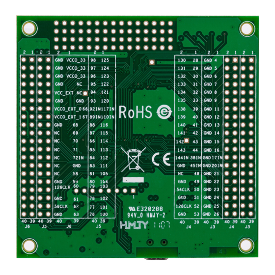
- Page 12 4256ZE Breakout Board Evaluation Kit User’s Guide Figure 4. J3/J4 Header Landing Callout Top Side J3 J4 17 IN 38 IN 144 IN 20 IN 45 IN 54 CLK 128 CLK Figure 5. J5/J6 Header Landing Callout Top Side...
- Page 13 The board features the ispMACH 4000ZE CPLD which is ideal for low-power, high-volume portable applications. The on-board ispMACH 4256ZE is the highest capacity device of the family with 256 macrocells (equivalent to about 450 FPGA LUTs). The 144-pin TQFP package provides 96 user I/Os and 4 dedicated inputs in a 20mm x 20mm package.
- Page 14 The USB mini-B socket of the Breakout Board serves as the programming and debug interface. JTAG Programming: For JTAG programming, a preprogrammed USB PHY peripheral controller is provided on the Breakout Board to serve as the programming interface to the ispMACH 4256ZE CPLD. Programming requires the ispVM System software.
-
Page 15: Board Modifications
4256ZE Breakout Board Evaluation Kit User’s Guide Board Modifications This section describes modifications to the board to change or add functionality. Bypassing the USB Programming Interface The USB programming interface circuit (section 6.2.8 USB Programming and Debug Interface) may be optionally bypassed by removing the 0 ohm resistors: R3, R4, R7, and R9 (See Schematic Sheet 2 of 4, Appendix A. -
Page 16: Troubleshooting
Evaluation Kit User’s Guide Troubleshooting Use the tips in this section to diagnose problems with the ispMACH 4256ZE Breakout Board. LEDs Do Not Flash If power is applied but the board does not flash according to the preprogrammed counter demonstration then it is likely that the board has been reprogrammed with a new design. -
Page 17: Ordering Information
01.1 Added Appendix C. Known Issues. © 2012 Lattice Semiconductor Corp. All Lattice trademarks, registered trademarks, patents, and disclaimers are as listed at www.latticesemi.com/legal. All other brand or product names are trademarks or registered trademarks of their respective holders. The specifications and information herein are subject to change without notice. -
Page 18: Appendix A. Schematics
4256ZE Breakout Board Evaluation Kit User’s Guide Appendix A. Schematics Figure 7. ispMACH 4256ZE Breakout Board, Cover... - Page 19 4256ZE Breakout Board Evaluation Kit User’s Guide Figure 8. USBIF to JTAG...
- Page 20 4256ZE Breakout Board Evaluation Kit User’s Guide Figure 9. Connectors and LEDs...
- Page 21 4256ZE Breakout Board Evaluation Kit User’s Guide Figure 10. ispMACH 4000ZE...
-
Page 22: Appendix B. Bill Of Materials
4256ZE Breakout Board Evaluation Kit User’s Guide Appendix B. Bill of Materials Table 12. Bill of Materials, ispMACH 4256ZE Breakout Board Item Quantity Reference Part Number C2, C4, C5, C6, C7, C8, C9, C13, C14, C15, C17, C20, C21, C22, C23,... -
Page 23: Appendix C. Known Issues
1. The ispMACH 4000ZE 1532 interface signals TCK, TMS, TDI and TDO are referenced to VCC=1.8V (logic core). The ispMACH 4256ZE Breakout Board has an issue where the JTAG signals are connected to the FTDI which has a 3.3V interface. This circuit should not be replicated in a production board. As a work-around another FTDI device could be selected or a level translator could be used between the FTDI device and the ispMACH 4000ZE. - Page 24 Mouser Electronics Authorized Distributor Click to View Pricing, Inventory, Delivery & Lifecycle Information: Lattice LC4256ZE-P-EVN LC4256ZE-B-EVN...
Need help?
Do you have a question about the ispMACH 4256ZE and is the answer not in the manual?
Questions and answers