Lattice Semiconductor MachXO2 User Manual
Breakout board evaluation kit
Hide thumbs
Also See for MachXO2:
- Programming and configuration usage manual (58 pages) ,
- User manual (41 pages) ,
- Usage manual (11 pages)

Related Manuals for Lattice Semiconductor MachXO2


Summary of Contents for Lattice Semiconductor MachXO2
- Page 1 MachXO2 Breakout Board Evaluation Kit User’s Guide February 2013 Revision: EB68_02.0...
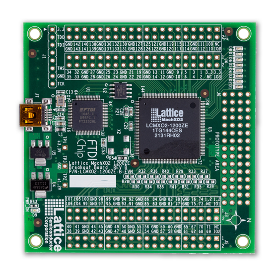
- Page 2 The MachXO2 Breakout Board currently features the MachXO2-7000HE device. A previous version of this board featured the MachXO2-1200ZE. The board design and features have not changed, and consequently, this docu- ment can be used as a guide for either version of the board. If you require a board featuring the MachXO2-1200ZE, Lattice recommends the MachXO2 Pico Development Kit.
-
Page 3: Storage And Handling
• FTDI Chip USB hardware drivers (installed as an option within the Diamond installation program) MachXO2 Device This board currently features the MachXO2-7000HE FPGA which offers embedded Flash technology for instant- on, non-volatile operation in a single chip. Numerous system functions are included, such as two PLLs and 256 Kbits of embedded RAM plus hardened implementations of I C, SPI, timer/counter, and user Flash memory. -
Page 4: Demonstration Design
Evaluation Kit User’s Guide 114 user I/Os in a 20mm x 20mm form factor. Previous versions of this board featured the MachXO2-1200ZE PLD in the same package. This version of the board is no longer available. A complete description of this device can be... -
Page 5: Download Demo Designs
Programming a Demo Design with the Lattice Diamond Programmer The demonstration design is pre-programmed into the MachXO2 Breakout Board by Lattice. If you have changed the design but now want to restore the Breakout Board to factory settings, use the procedure described below. -
Page 6: Machxo2 Breakout Board
This section describes the features of the MachXO2 Breakout Board in detail. Overview The Breakout Board is a complete development platform for the MachXO2 FPGA. The board includes a prototyping area, a USB program/power port, an LED array, and header landings with electrical connections to most of the FPGA’s programmable I/O, power, and JTAG pins. - Page 7 This section describes the principle sub systems for the Breakout Board in alphabetical order. Clock Sources All clocks for the counter demonstration designs originate from the MachXO2 on-chip oscillator. You may use an expansion header landing to drive a FPGA input with an external clock source.
- Page 8 MachXO2 Breakout Board Evaluation Kit User’s Guide Table 3. Expansion Header Pin Information (J2) Header Pin Number -1200ZE Function -7000HE Function MachXO2 Pin VCCIO0 VCCIO0 118, 123, 135 PT17D / DONE PT36D / DONE PT17C / INITn PT36C / INITn...
- Page 9 MachXO2 Breakout Board Evaluation Kit User’s Guide Table 4. Expansion Header Pin Information (J3) Header Pin Number -1200ZE Function -7000HE Function MachXO2 Pin VCC_1.2V VCC_1.2V 36, 72, 108, 144 VCCIO1 VCCIO1 79, 88, 102 VCC_1.2V VCC_1.2V 36, 72, 108, 144...
- Page 10 MachXO2 Breakout Board Evaluation Kit User’s Guide Table 5. Expansion Header Pin Information (J4) Header Pin Number -1200ZE Function -7000HE Function MachXO2 Pin VCC_3.3V VCC_3.3V VCCIO3 VCCIO3/4/5 30, 16, 7 VCC_3.3V VCC_3.3V PL2A / L_GPLLT_FB PL3A / L_GPLLT_FB PL2B / L_GPPLC_FB...
- Page 11 MachXO2 Breakout Board Evaluation Kit User’s Guide Table 6. Expansion Header Pin Information (J5) Header Pin Number -1200ZE Function -7000HE Function MachXO2 Pin VCCIO2 VCCIO2 37, 51, 66 PB20D / SI / SISPI PB38B / SI / SISPI PB20B PB37B...
- Page 12 MachXO2 Breakout Board Evaluation Kit User’s Guide Figure 4. J2/J4 Header Landing Callout Top Side Figure 5. J3/J5 Header Landing Callout Top Side...
- Page 13 4TG144C MachXO2 FPGA The MachXO2-7000HE-4TG144C is a 144-pin TQFP package FPGA device which provides up to 114 usable I/Os in a 20 x 20mm package. 108 I/Os are accessible from the breakout board headers. Table 7. MachXO FPGA Interface Reference...
- Page 14 Test Mode Select 130:TMS Test Clock 131:TCK LEDs A green LED (D9) is used to indicate USB 5V power. Eight red LEDs are driven by I/O pins of the MachXO2 device. Table 10. Power and User LEDs Reference Item Description Reference Designators...
-
Page 15: Troubleshooting
Measuring Bank and Core Power In addition to the expansion headers, test points (TP1, TP2) provide access to power supplies of the MachXO2 FPGA. Inline 1 ohm resistors: R24 (VCCIO0, +3.3V, Bank 0), R25 (VCCIO1, +3.3V, Bank 1), R26 (VCCIO2, +3.3V, Bank 2), R27 (VCCIO3, +3.3V, Bank 3), R56 (VCC core, +1.2V) can be used to measure current for the power sup-... -
Page 16: Ordering Information
Ordering Information China RoHS Environment-Friendly Description Ordering Part Number Use Period (EFUP) MachXO2-7000HE Breakout Board Evaluation Kit LCMXO2-7000HE-B-EVN MachXO2 Breakout Board Evaluation Kit LCMXO2-1200ZE-B-EVN 1.For reference only. This version of the board is no longer available for sale. Technical Support Assistance... -
Page 17: Revision History
Updated Tables 3-6 to include -7000HE information. Added -7000HE notes to Figure 3 and Appendix A. © 2013 Lattice Semiconductor Corp. All Lattice trademarks, registered trademarks, patents, and disclaimers are as listed at www.latticesemi.com/legal. All other brand or product names are trademarks or registered trademarks of... -
Page 18: Appendix A. Schematics
Evaluation Kit User’s Guide Appendix A. Schematics Note: The schematics are drawn using the MachXO2-1200ZE device. Please consult Tables 3 through 6 for -1200 and -7000HE pin name and bank synonyms. Pin numbers are correct for either device. Figure 7. Block Diagram... - Page 19 MachXO2 Breakout Board Evaluation Kit User’s Guide Figure 8. USB Interface to JTAG...
- Page 20 MachXO2 Breakout Board Evaluation Kit User’s Guide Figure 9. FPGA...
- Page 21 MachXO2 Breakout Board Evaluation Kit User’s Guide Figure 10. FPGA...
- Page 22 MachXO2 Breakout Board Evaluation Kit User’s Guide Figure 11. Power LEDs...
-
Page 23: Appendix B. Bill Of Materials
MachXO2 Breakout Board Evaluation Kit User’s Guide Appendix B. Bill of Materials Table 12. MachXO2 Breakout Board Bill of Materials Item Quantity Reference Manufacturer Part Number C1, C3 Panasonic ECJ-1VB0J475K C2, C4, C5, C6, C7, C8, C9, C11, C12, C15, C16, C18,... - Page 24 Mouser Electronics Authorized Distributor Click to View Pricing, Inventory, Delivery & Lifecycle Information: Lattice LCMXO2-1200ZE-B-EVN...
Need help?
Do you have a question about the MachXO2 and is the answer not in the manual?
Questions and answers