
Subscribe to Our Youtube Channel
Related Manuals for Lattice Semiconductor LatticeECP2M SERDES


Summary of Contents for Lattice Semiconductor LatticeECP2M SERDES
- Page 1 LatticeECP2M™ SERDES Evaluation Board User’s Guide May 2010 Revision: EB25_01.7...
-
Page 2: Board Features
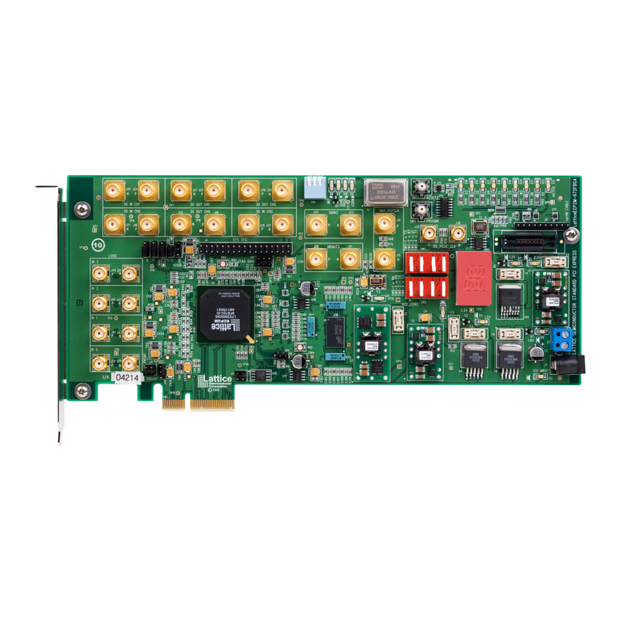
FPGA. The intended use of this guide is to be referenced in conjunction with evaluation design tutorials to demon- strate the LatticeECP2M FPGA. Figure 1. LatticeECP2M SERDES Evaluation Board Board Features • LatticeECP2M FPGA in 672-ffBGA package. Default device is LFE2M35E-6FF672C. - Page 3 However it remains the user's responsibility to verify proper and reliable operation of Lattice products in their end application by consulting documentation provided by Lattice. Differences in component selection and/or PCB layout in the user's application may significantly affect circuit performance and reliability. Figure 2. LatticeECP2M SERDES Evaluation Board Block Diagram 16 SMAs/ LatticeECP2M-50 Only...
-
Page 4: Latticeecp2M Device
Applying Power to the Board The LatticeECP2M SERDES Evaluation Board is ready to power on. The board can be supplied with power from an AC wall-type transformer power supply shipped with the board. Or it can be supplied from a bench-top supply via terminal screw connections. -
Page 5: Pci Express Power Interface
LatticeECP2M SERDES Lattice Semiconductor Evaluation Board User’s Guide Table 1. Board Power Supply Fuses (see Appendix A, Figure 4) 1.2V Core Fuse 1.5V Fuse 3.3V Fuse 1.2V Fuse 2.5V Fuse 1.8V Fuse Table 2. Board Power Supply Indicators (see Appendix A, Figure 4) 2.5V Source Good Indicator... -
Page 6: Programming Daisy Chain
Programming Daisy Chain This board includes two Lattice Semiconductor programmable devices that can be programmed in a daisy chain. A jumper setting of J105 controls the chain. Both devices are in the programming chain from the JTAG header J8 with jumpers on J105 across pins {1-2}, pins{3-4} and pins{5-6}. - Page 7 LatticeECP2M SERDES Lattice Semiconductor Evaluation Board User’s Guide 1. Press the SCAN button located in the toolbar. The LatticeECP2M device will automatically be detected. 2. Double-click the device to open the device information dialog. In the device information dialog, click the Browse button located under Data File.
-
Page 8: Configuration Status Indicators
LatticeECP2M SERDES Lattice Semiconductor Evaluation Board User’s Guide Configuration Status Indicators (see Appendix A, Figure 4) These LEDs indicate the status of configuration to the FPGA. • D8 (red) illuminated – Indicates that programming was aborted or reinitialized, driving the INITN output low. - Page 9 LatticeECP2M SERDES Lattice Semiconductor Evaluation Board User’s Guide Table 5. SMA Clock Input Signal U2 Reference + Input U2 Reference - Input U2 is an ispClock5620A clock generator that allows designers to implement clock distribution networks supporting multiple, synchronized output frequencies using a single device. By integrating a Phase-Locked Loop (PLL) along with multiple output dividers, the ispClock5620A can derive up to five separate output frequencies from a single ®...
- Page 10 LatticeECP2M SERDES Lattice Semiconductor Evaluation Board User’s Guide SERDES (see Appendix A, Figure 5) SERDES Reference Clock The 50-ohm terminated SMA connectors provide supply reference clocks directly to the LatticeECP2M device from the ispClock management device. This device drives clocks to both SERDES quads via 100-ohm LVDS signaling.
-
Page 11: Fpga Test Pins
LatticeECP2M SERDES Lattice Semiconductor Evaluation Board User’s Guide SERDES SATA Channels (see Appendix A, Figure 5) Connections are included to attach SATA type cables to SERDES channels for board-to-board or loopback pur- poses. The connectors are configured using the 7-pin SATA specifications. Note: this interface is only available on boards featuring a LatticeECP2M-50 or larger FPGA. -
Page 12: Test Sma Connections
LatticeECP2M SERDES Lattice Semiconductor Evaluation Board User’s Guide Figure 4. 17-Segment LED Display Segment K M N Test SMA Connections General-purpose FPGA pins are available via SMA test connections. These connections are designed to permit evaluations of several types of FPGA I/O buffers. The use of several termination schemes permits easy interfaces for the type of buffer. -
Page 13: Test Pad Array
DDR2 Memory (see Appendix A, Figure 10) The LatticeECP2M SERDES Evaluation Board is equipped with an 84-ball BGA DDR2 SDRAM memory device such as the Micron MT47H16M16BG-3 device. The DDR2 memory interface includes a 16-bit wide device. The evaluation board includes termination of address and command signals. It includes all power and external compo-... -
Page 14: Ordering Information
01.7 Updated Known Issues section. © 2010 Lattice Semiconductor Corp. All Lattice trademarks, registered trademarks, patents, and disclaimers are as listed at www.latticesemi.com/legal. All other brand or product names are trademarks or registered trademarks of their respective holders. The specifications and information herein are subject to change without notice. -
Page 15: Appendix A. Schematic
LatticeECP2M SERDES Lattice Semiconductor Evaluation Board User’s Guide Appendix A. Schematic Figure 5. Cover Page... - Page 16 LatticeECP2M SERDES Lattice Semiconductor Evaluation Board User’s Guide Figure 6. DC/DC Conversion...
- Page 17 LatticeECP2M SERDES Lattice Semiconductor Evaluation Board User’s Guide Figure 7. Power Supplies...
- Page 18 LatticeECP2M SERDES Lattice Semiconductor Evaluation Board User’s Guide Figure 8. Configuration/Testpoints...
- Page 19 LatticeECP2M SERDES Lattice Semiconductor Evaluation Board User’s Guide Figure 9. SERDES...
- Page 20 LatticeECP2M SERDES Lattice Semiconductor Evaluation Board User’s Guide Figure 10. DDR2 FPGA Controller DDR2_A[0:12]...
- Page 21 LatticeECP2M SERDES Lattice Semiconductor Evaluation Board User’s Guide Figure 11. DDR2 Device/Termination DDR2_A[0:12] DDR2_DQ[0:15] DDR2_A[0:12]...
- Page 22 LatticeECP2M SERDES Lattice Semiconductor Evaluation Board User’s Guide Figure 12. Clocks...
- Page 23 LatticeECP2M SERDES Lattice Semiconductor Evaluation Board User’s Guide Figure 13. Differential I/O Loops...
- Page 24 LatticeECP2M SERDES Lattice Semiconductor Evaluation Board User’s Guide Figure 14. FPGA Test...
- Page 25 LatticeECP2M SERDES Lattice Semiconductor Evaluation Board User’s Guide Figure 15. VSS/Decoupling...
Need help?
Do you have a question about the LatticeECP2M SERDES and is the answer not in the manual?
Questions and answers