Table of Contents
Advertisement
Quick Links
Advertisement
Table of Contents

Related Manuals for Lattice Semiconductor iCE40HX-8K


Summary of Contents for Lattice Semiconductor iCE40HX-8K
- Page 1 Breakout Board User’s Guide November 2013 EB85_01.0...
- Page 2 • Pre-loaded Demo – The kit comes with a default design that flashes the LEDs on and off • USB connector Cable – A mini B USB cable for programming the SRAM fabric of the iCE40HX-8K or the on- board SPI flash. The USB cable also powers the iCE40HX-8K evaluation board.
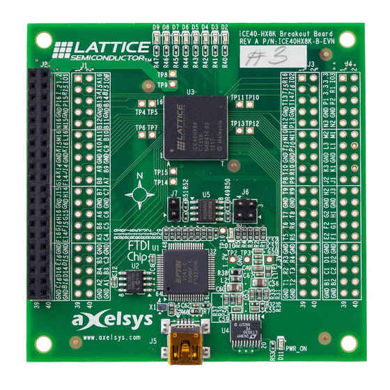
- Page 3 Breakout Board Figure 1. iCE40HX-8K Evaluation Board (Top Side) LEDs iCE40HX-8K 0.1" spaced holes 40 pin header Figure 2. Block Diagram HEADER I/Os LEDS(1-8) BANK 0 I/Os I/Os FPGA iCE40HX8K-CT256 USB to RS232 Power from USB 5V SPI / RS232...
-
Page 4: Ice40 Device
Breakout Board iCE40 Device This board features an iCE40HX-8K device with a 1.2v core supply. It is packaged in a 256 caBGA package. For a complete description of this device, see HB1011, iCE40 LP/LX/LM Family Handbook. Software Requirements You should install the following software before you begin developing designs for the evaluation board: •... -
Page 5: Board Power
Breakout Board Board Power The iCE40HX-8K evaluation board is powered with the USB cable. LED location D11 indicates that the board is powered up. All I/Os are driven at 3.3v. Board I/Os The I/Os that feed the holes and the 0.1” connector are driven at 3.3v levels. Location J2 is the populated 2 x 20 row connector. -
Page 6: Ordering Information
J6:1-2 and J6:3-4. Jumper J7 is not installed. See Figure 5 Figure 5. CRAM Programming LED in location D10 is connected to the CDONE pin of the iCE40HX-8K. This can be monitored to determine that the iCE40HX-8K is programmed correctly. -
Page 7: Technical Support Assistance
01.0 Initial release. © 2013 Lattice Semiconductor Corp. All Lattice trademarks, registered trademarks, patents, and disclaimers are as listed at www.latticesemi.com/legal. All other brand or product names are trademarks or registered trademarks of their respective holders. The specifications and information herein are subject to change without notice. -
Page 8: Appendix A. Schematic Diagrams
Appendix A. Schematic Diagrams Figure 6. Block Diagram BANK 3... - Page 9 Figure 7. USB to SPI/RS232...
- Page 10 Figure 8. FPGA...
- Page 11 Figure 9. FPGA...
- Page 12 Figure 10. Power and LEDs...
- Page 13 Figure 11. SPI...
- Page 14 Mouser Electronics Authorized Distributor Click to View Pricing, Inventory, Delivery & Lifecycle Information: Lattice ICE40HX8K-B-EVN...