
Related Manuals for Lattice Semiconductor LatticeECP2M PCI Express x4


Summary of Contents for Lattice Semiconductor LatticeECP2M PCI Express x4
- Page 1 LatticeECP2M™ PCI Express x4 Evaluation Board User’s Guide February 2008 Revision: EB22_01.6...
- Page 2 Evaluation Board User’s Guide Introduction This user’s guide describes the LatticeECP2M PCI Express x4 Evaluation Board featuring the LatticeECP2M FPGA device. The evaluation board has been designed to support the LatticeECP2M35 device and the LatticeECP2M50 device. Different versions of the evaluation board are available that contain either the LatticeECP2M35 device or the LatticeECP2M50 device.
-
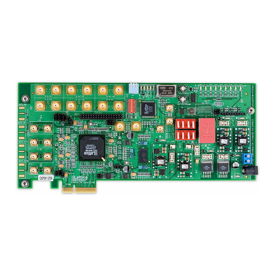
Page 3: Board Features
Figure 1 shows the functional partitioning of the board. Figure 2. LatticeECP2M PCI Express x4 Evaluation Board SMAs for a Single 1 Quad of 3G... -
Page 4: Latticeecp2M Device
Applying Power to the Board The LatticeECP2M PCI Express x4 Evaluation Board is ready to power on. The board can be supplied with power from an AC wall-type transformer power supply shipped with the board. Or it can be supplied from a bench top sup- ply via terminal screw connections. -
Page 5: Pci Express Power Interface
LatticeECP2M PCI Express x4 Lattice Semiconductor Evaluation Board User’s Guide All input power sources and on-board power supplies are fused with surface mounted fuses and have green LEDs to indicate power GOOD status of the intermediate supplies Table 1. Board Power Supply Fuses (see Appendix A, Figure 6) 1.2V Core Fuse... -
Page 6: Programming Daisy Chain
LatticeECP2M PCI Express x4 Lattice Semiconductor Evaluation Board User’s Guide Table 4. ispVM JTAG Connector (see Appendix A, Figure 8) Pin 1 Pin 2 Pin 3 Pin 4 PROGRAMN Pin 5 Pin 6 Pin 7 Pin 8 Pin 9 DONE... - Page 7 LatticeECP2M PCI Express x4 Lattice Semiconductor Evaluation Board User’s Guide 4. Press the SCAN button located in the toolbar. The LatticeECP2M device should be automatically detected. 5. Double-click the device to open the device information dialog. In the device information dialog, click the Browse button located under Data File .
-
Page 8: Fpga Clock Management
LatticeECP2M PCI Express x4 Lattice Semiconductor Evaluation Board User’s Guide Configuration Status Indicators (see Appendix A, Figure 8) These LEDs indicate the status of configuration to the FPGA. • D8 (RED) illuminated, this indicates that the programming was aborted or reinitialized driving the INITN output low. - Page 9 LatticeECP2M PCI Express x4 Lattice Semiconductor Evaluation Board User’s Guide ® separate output frequencies from a single input reference frequency. PAC-Designer software (available from the Lattice web site at www.latticesemi.com/pacdesigner) is used to program the ispClock features. ispClock supports reference clocks in the range of 10 to 320 MHz. The duty cycle of the clock source need not be 50%;...
-
Page 10: Serdes Smpte Channels
LatticeECP2M PCI Express x4 Lattice Semiconductor Evaluation Board User’s Guide Table 5. SERDES Connectors (see Appendix A, Figure 9) Channel Name Channel Name L_HDINP0 L_HDOUTP0 L_HDINN0 L_HDOUTN0 L_HDINP1 L_HDOUTP1 L_HDINN1 L_HDOUTN1 L_HDINP2 L_HDOUTP2 L_HDINN2 L_HDOUTN2 SERDES SMPTE Channels Note: SERDES SMPTE channels are available only for the LFE2M50E-FF672 (or larger) device. - Page 11 LatticeECP2M PCI Express x4 Lattice Semiconductor Evaluation Board User’s Guide Note: LEDs will illuminate if connected to an unprogrammed FPGA pin. It is recommended that a pull-down be pro- grammed on FPGA output pins. 17-Segment LED Display (see Appendix A, Figure 14) General-purpose FPGA pins are connected to a 17-segment display according to the following table.
- Page 12 LatticeECP2M PCI Express x4 Lattice Semiconductor Evaluation Board User’s Guide Table 8. FPGA I/O Test SMA Connectors (see Appendix A, Figure 13) (Continued) LFE2M35E Termination Termination Designation Name Signal 672-BGA Description Resistor(s) LVDS_OUTN1 PR53B LVDS_OUTP2 PR55A 100-ohm Differential R135 LVDS_OUTN2...
-
Page 13: Ordering Information
01.6 Updated board photo. © 2008 Lattice Semiconductor Corp. All Lattice trademarks, registered trademarks, patents, and disclaimers are as listed at www.latticesemi.com/legal. All other brand or product names are trademarks or registered trademarks of their respective holders. The specifications and information herein are subject to change without notice. -
Page 14: Appendix A. Schematics
LatticeECP2M PCI Express x4 Lattice Semiconductor Evaluation Board User’s Guide Appendix A. Schematics Figure 5. Cover Page... - Page 15 LatticeECP2M PCI Express x4 Lattice Semiconductor Evaluation Board User’s Guide Figure 6. DC/DC Conversion...
- Page 16 LatticeECP2M PCI Express x4 Lattice Semiconductor Evaluation Board User’s Guide Figure 7. Power Supplies...
- Page 17 LatticeECP2M PCI Express x4 Lattice Semiconductor Evaluation Board User’s Guide Figure 8. Configuration/Testpoints...
- Page 18 LatticeECP2M PCI Express x4 Lattice Semiconductor Evaluation Board User’s Guide Figure 9. SERDES...
- Page 19 LatticeECP2M PCI Express x4 Lattice Semiconductor Evaluation Board User’s Guide Figure 10. DDR2 FPGA Controller DDR2_A[0:12]...
- Page 20 LatticeECP2M PCI Express x4 Lattice Semiconductor Evaluation Board User’s Guide Figure 11. DDR2 Device/Termination DDR2_A[0:12] DDR2_DQ[0:15] DDR2_A[0:12]...
- Page 21 LatticeECP2M PCI Express x4 Lattice Semiconductor Evaluation Board User’s Guide Figure 12. Clocks...
- Page 22 LatticeECP2M PCI Express x4 Lattice Semiconductor Evaluation Board User’s Guide Figure 13. Differential I/O Loops...
- Page 23 LatticeECP2M PCI Express x4 Lattice Semiconductor Evaluation Board User’s Guide Figure 14. FPGA Test...
- Page 24 LatticeECP2M PCI Express x4 Lattice Semiconductor Evaluation Board User’s Guide Figure 15. VSS/Decoupling...
Need help?
Do you have a question about the LatticeECP2M PCI Express x4 and is the answer not in the manual?
Questions and answers