Table of Contents
Advertisement
Quick Links
Advertisement
Table of Contents

Related Manuals for Lattice Semiconductor MachXO3


Summary of Contents for Lattice Semiconductor MachXO3
- Page 1 MachXO3 Starter Kit User Guide EB95 Version 1.2, March 2016...
- Page 2 Thank you for choosing the Lattice Semiconductor MachXO3 Starter Kit! This user’s guide describes how to start using the MachXO3 Starter Kit, an easy-to-use platform for evaluating and designing with the MachXO3 ultra-low density FPGA. Along with the board and accessories, this kit includes a pre- loaded demonstration design.
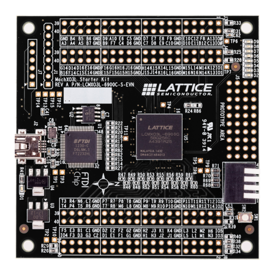
- Page 3 MachXO3 Starter Kit User Guide Figure 1. MachXO3 Board (MachXO3L Version), Top Side Two 2 x 20 Header Landings (J3, J4) JTAG Header Landing (J1) LED array (D9-D2) SPI/I2C Header Landing (J7) MachXO3L PLD 4 x 10 40-Hole (U5) Prototype array...
-
Page 4: Storage And Handling
MachXO3 Starter Kit User Guide Figure 2. MachXO3 Board (MachXO3L Version), Bottom Side SPI Flash Boot Memory (U6) Storage and Handling Static electricity can shorten the lifespan of electronic components. Please observe these tips to prevent damage that could occur from electro-static discharge: •... -
Page 5: Demonstration Design
Upon power-up, the preprogrammed demonstration design automatically loads and drives the LED array in a 1-hertz pattern. The program shows a clock divider driven either by the MachXO3 internal oscillator or the external FTDI clock chip. The divider modules (heartbeat.v and kitcar.v) are clocked at the default frequency of 12 MHz which divides the clock to cycle the LED display approximately once per second. -
Page 6: Download Demo Designs
MachXO3 Starter Kit User Guide To load the FTDI Chip USB hardware drivers as part of the Lattice Diamond installation: 1. Select Programmer Drivers in the Product Options of Lattice Diamond Setup. 2. Select FTDI Windows USB Driver or All Drivers in the LSC Drivers Install/Uninstall dialog box. -
Page 7: Programming A Demo Design With The Lattice Diamond Programmer
Programming a Demo Design with the Lattice Diamond Programmer The demonstration design is pre-programmed into the MachXO3 board by Lattice. If you have changed the design but now want to restore the board to factory settings, use the procedure described below. -
Page 8: Machxo3 Starter Kit
This section describes the features of the MachXO3 Starter Kit in detail. Overview The Starter Kit is a complete development platform for the MachXO3 FPGA. The board includes a prototyping area, a USB program/power port, an LED array, switches, and header landings with electrical connections to most of the FPGA’s programmable I/O, power, and configuration pins. - Page 9 This section describes the principle sub systems for the Starter Kit in alphabetical order. Clock Sources Clock sources for the LED demonstration designs originate from the MachXO3 on-chip oscillator or the 12 MHz crystal X1. You may use an expansion header landing to drive a FPGA input with an external clock source.
- Page 10 MachXO3 Starter Kit User Guide Table 4. Expansion Header Pin Information (J3) Header Pin Number –6900C Function MachXO3 Ball VCCIO0 D5,D12,G8,G9 VCCIO0 D5,D12,G8,G9 PT36C/INITn PT36D/DONE PT22A PT35B PT35A PT26B PT27B PT27A — — PT26A PT27C/JTAGENB PT17B PT21B PT14B PT21A PT16B PT15B —...
- Page 11 MachXO3 Starter Kit User Guide Table 5. Expansion Header Pin Information (J4) Header Pin Number –6900C Function MachXO3 Ball VCCIO1 E13,H10,J10,M13 VCCIO1 E13,H10,J10,M13 PR19D PR19C PR23A PR24B PR18B PR24A PR23B PR21B — — PR21A PR18A PR17A PR16B PR17B PR15B PR12A/PCLKT1_0 PR16A —...
- Page 12 MachXO3 Starter Kit User Guide Table 6. Expansion Header Pin Information (J6) Header Pin Number –6900C Function MachXO3 Ball VCCIO2 K8,K9,N5,N12 VCCIO2 K8,K9,N5,N12 PB35B PB34B PB35A PB34A PB31A PB28B PB31B PB28A — — PB26B PB29A PB26A PB29B PB23A/PCLKT2_1 PB21B PB23B/PCLKC2_1 PB21A —...
- Page 13 MachXO3 Starter Kit User Guide Table 7. Expansion Header Pin Information (J8) Header Pin Number –6900C Function MachXO3 Ball VCCIO5 VCCIO3 PL9D PL25B PL25A PL22B/PCLKC3_0 PL22A/PCLKT3_0 PL19A PL19B PL19D — — PL19C PL12A/PCLKT4_0 PL15B PL15A PL12B/PCLKC4_0 PL11A PL10B PL11B —...
- Page 14 MachXO3 Starter Kit User Guide Figure 5. J3/J4 Header Landing Callout Top Side VCCIO0 VCCIO0 VCCIO1 VCCIO1 Figure 6. J6/J8 Header Landing Callout Top Side VCCIO2 VCCIO2 VCCIO5 VCCIO3 VCCIO4...
- Page 15 The LCMXO3L/LF-6900C-5BG256C is a 256-ball caBGA package FPGA device which provides up to 206 usable I/Os in a 14 mm x 14 mm package. 150 I/Os are accessible from the board headers, switches and LEDs. Table 8. MachXO3 FPGA Interface Reference Item...
- Page 16 C9:SDA Serial Clock A9:SCL LEDs A blue LED (D1) is used to indicate USB 5V power. Eight red LEDs are driven by I/O pins of the MachXO3 device. Table 13. Power and User LEDs Reference Item Description Red LEDs (D2, D3, D4, D5, D6, D7, D8, D9)
-
Page 17: Board Modifications
Measuring Bank and Core Power Test points (TP1, TP2) provide access to power supplies of the MachXO3 FPGA. Inline 1 Ohm resistors: R31 (VCCIO0, +3.3 V, Bank 0), R25 (VCCIO1, +3.3 V, Bank 1), R37 (VCCIO2, +3.3 V, Bank 2), R32 (VCCIO3, +3.3 V, Bank 3), R26 (VCCIO4, +3.3 V, Bank 4), R38 (VCCIO5, +3.3 V, Bank 5), R24 (VCC core, +1.2 V) can be used to mea-... -
Page 18: Troubleshooting
MachXO3 Starter Kit User Guide Troubleshooting Use the tips in this section to diagnose problems with the Starter Kit. LEDs Do Not Flash If power is applied but the board does not flash according to the preprogrammed counter demonstration then it is likely the board has been reprogrammed with a new design. -
Page 19: Ordering Information
November 2014 Initial release. © 2016 Lattice Semiconductor Corp. All Lattice trademarks, registered trademarks, patents, and disclaimers are as listed at www.latticesemi.com/legal. All other brand or product names are trademarks or registered trademarks of their respective holders. The specifications and information herein are subject to change without notice. -
Page 20: Appendix A. Schematics
MachXO3 Starter Kit User Guide Appendix A. Schematics Figure 8. Block Diagram... - Page 21 MachXO3 Starter Kit User Guide Figure 9. USB Interface to JTAG...
- Page 22 MachXO3 Starter Kit User Guide Figure 10. FPGA...
- Page 23 MachXO3 Starter Kit User Guide Figure 11. FPGA...
- Page 24 MachXO3 Starter Kit User Guide Figure 12. Power LEDs...
- Page 25 MachXO3 Starter Kit User Guide Figure 13. Bank 2 I/O...
- Page 26 MachXO3 Starter Kit User Guide Figure 14. Bank 3, 4, 5 I/O...
- Page 27 MachXO3 Starter Kit User Guide Figure 15. Power Decoupling and LEDs...
-
Page 28: Appendix B. Bill Of Materials
MachXO3 Starter Kit User Guide Appendix B. Bill of Materials Table 15. MachXO3 Starter Kit Bill of Materials Item Quantity Reference Value Manufacturer MFG Pin C1,C3 4.7 uF Panasonic ECJ-1VB0J475K C2,C4,C6,C7,C10,C11,C12,C13,C14 0.1 uF Kemet C0402C104K4RACTU ,C15,C16,C21,C23,C24,C25,C26,C2 7,C28,C30,C31,C32,C33,C34,C36,C 37,C38,C39,C40,C42,C43,C44,C45, C46,C47,C48,C49,C50,C53,C54, C55,C56,C58,C59,C63... - Page 29 MachXO3 Starter Kit User Guide Table 15. MachXO3 Starter Kit Bill of Materials (Continued) Item Quantity Reference Value Manufacturer MFG Pin On Semi NCP1117ST33T3G Lattice Semiconductor LCMXO3L-6900C- 5BG256C or LCMXO3LF- 6900C-5BG256C Spansion S25FL204K0TMFI041 (early builds) or S25FL208K0RMFI041 (later builds) 12 MHz...
- Page 30 Mouser Electronics Authorized Distributor Click to View Pricing, Inventory, Delivery & Lifecycle Information: Lattice LCMXO3LF-6900C-S-EVN LCMXO3L-6900C-S-EVN...
Need help?
Do you have a question about the MachXO3 and is the answer not in the manual?
Questions and answers