Table of Contents
Advertisement
EP-MVP3G-M
EP-MVP3G-M
EP-MVP3G-M
EP-MVP3G-M
EP-MVP3G-M
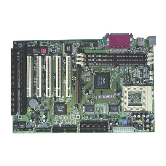
EP-MVP3G2
EP-MVP3G2
EP-MVP3G2
EP-MVP3G2
EP-MVP3G2
EP-MVP3G5
EP-MVP3G5
EP-MVP3G5
EP-MVP3G5
EP-MVP3G5
ISA/PCI/A
ISA/PCI/A
ISA/PCI/A
ISA/PCI/A GP Mainboar
ISA/PCI/A
Onboar
Onboar
d PCI IDE and Super
Onboar d PCI IDE and Super
d PCI IDE and Super
Onboar
Onboar
d PCI IDE and Super
Multi-I/O
Multi-I/O
Multi-I/O
Multi-I/O
Multi-I/O
TRADEMARK
All products and company names are trademarks or registered
trademarks of their respective holders.
These specifications are subject to change without notice.
GP Mainboar
GP Mainboar
GP Mainboar d with
GP Mainboar
d PCI IDE and Super
Manual Revision 10.1
September 2, 1999
d with
d with
d with
d with
Advertisement
Table of Contents


Need help?
Do you have a question about the EP-MVP3G-M and is the answer not in the manual?
Questions and answers