Table of Contents
Advertisement
Advertisement
Table of Contents

Subscribe to Our Youtube Channel
Related Manuals for EUROCOM N150SC

Summary of Contents for EUROCOM N150SC
- Page 1 4...
- Page 3 Preface Notebook Computer N150SC / N150SD Service Manual...
- Page 4 Preface Notice The company reserves the right to revise this publication or to change its contents without notice. Information contained herein is for reference only and does not constitute a commitment on the part of the manufacturer or any subsequent ven- dor.
- Page 5 This manual is intended for service personnel who have completed sufficient training to undertake the maintenance and inspection of personal computers. It is organized to allow you to look up basic information for servicing and/or upgrading components of the N150SC / N150SD series notebook PC.
- Page 6 Preface IMPORTANT SAFETY INSTRUCTIONS Follow basic safety precautions, including those listed below, to reduce the risk of fire, electric shock and injury to per- sons when using any electrical equipment: 1. Do not use this product near water, for example near a bath tub, wash bowl, kitchen sink or laundry tub, in a wet basement or near a swimming pool.
-
Page 7: Instructions For Care And Operation
Preface Instructions for Care and Operation The notebook computer is quite rugged, but it can be damaged. To prevent this, follow these suggestions: Don’t drop it, or expose it to shock. If the computer falls, the case and the components could be damaged. Do not expose the computer Do not place it on an unstable Do not place anything heavy... -
Page 8: Power Safety
Preface Avoid interference. Keep the computer away from high capacity transformers, electric motors, and other strong mag- netic fields. These can hinder proper performance and damage your data. Take care when using peripheral devices. Use only approved brands of Unplug the power cord before peripherals. -
Page 9: Battery Precautions
Preface Battery Precautions • Only use batteries designed for this computer. The wrong battery type may explode, leak or damage the computer. • Do not continue to use a battery that has been dropped, or that appears damaged (e.g. bent or twisted) in any way. Even if the computer continues to work with a damaged battery in place, it may cause circuit damage, which may possibly result in fire. -
Page 10: System Startup
Preface Related Documents You may also need to consult the following manual for additional information: User’s Manual on CD/DVD This describes the notebook PC’s features and the procedures for operating the computer and its ROM-based setup pro- gram. It also describes the installation and operation of the utility programs provided with the notebook PC. System Startup 1. -
Page 11: Table Of Contents
Preface Contents Introduction ..........1-1 Bottom ................... A-4 Main Board ................... A-5 Overview ..................1-1 HDD ....................A-6 Specifications ..................1-2 2nd HDD ..................A-7 External Locator - Top View with LCD Panel Open ......1-4 LCD ....................A-8 External Locator - Front & Right Side Views .........1-5 DVD .................... - Page 12 Preface Lynx 1/9 ..................B-23 ODD Ext. Board ................B-55 Lynx 2/9 ..................B-24 Power Sequence ................B-56 Updating the FLASH ROM BIOS..C-1 Lynx 3/9 ..................B-25 Lynx 4/9 ..................B-26 Download the BIOS ................C-1 Lynx 5/9 ..................B-27 Unzip the downloaded files to a bootable CD/DVD or Lynx 6/9 ..................
-
Page 13: Introduction
Chapter 1: Introduction Overview This manual covers the information you need to service or upgrade the N150SC / N150SD series notebook computer. Information about operating the computer (e.g. getting started, and the Setup utility) is in the User’s Manual. Information about dri-vers (e.g. -
Page 14: Specifications
Introduction Specifications Processor Options Storage Design I: (Factory Option) One 9.5mm(h) Optical Device Type Drive (Super Multi Drive) Intel® Core™ i7 Processor (Factory Option) 2.5" 9.5mm 2nd HDD/SSD caddy i7-4720HQ (2.60GHz) One Changeable 2.5" 9.5mm/7.0mm (h) SATA HDD/SSD 6MB L3 Cache, 22nm, DDR3L-1600MHz, TDP 47W Latest Specification Information Intel®... - Page 15 Introduction NVIDIA® Discrete GPU M.2 Slots Power NVIDIA® GeForce GTX 960M Slot 1 for M.2 2230 WLAN Combo Module Card with PCIe & Full Range AC/DC Adapter 2GB GDDR5 Video RAM on board USB Interfaces AC Input: 100 - 240V, 50 - 60Hz Microsoft DirectX®...
-
Page 16: External Locator - Top View With Lcd Panel Open
Introduction External Locator - Top View with LCD Panel Open Figure 1 Top View 1. PC Camera 2. *PC Camera LED *When the PC camera is in use, the LED will be illuminated. 3. Microphone 4. LCD 5. Speakers 6. Power Button 7. -
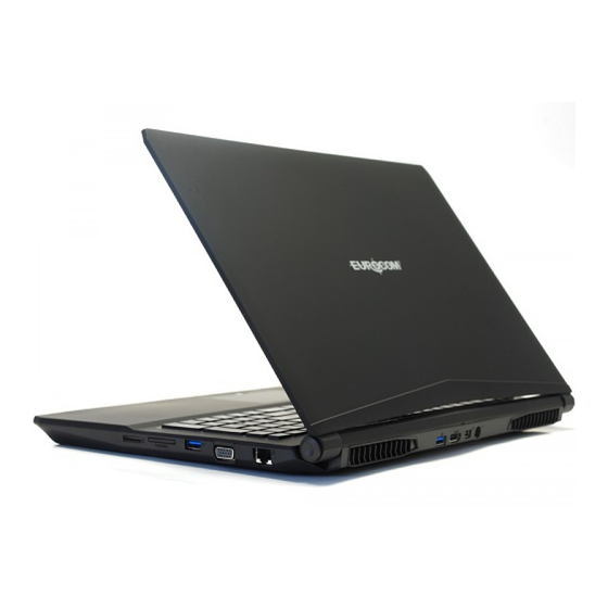
Page 17: External Locator - Front & Right Side Views
Introduction External Locator - Front & Right Side Views Figure 2 Front View 1. LED Indicators FRONT VIEW Figure 3 Right Side View 1. USIM Card RIGHT SIDE VIEW Reader (for 3G/ 4G USIM Cards) 2. Multi-in-1 Card Reader 3. USB 3.0 Port 4. -
Page 18: External Locator - Left Side & Rear View
Introduction External Locator - Left Side & Rear View Figure 4 Left Side View 1. Security Lock Slot 2. USB 3.0 Ports 3. S/PDIF-Out Jack LEFT SIDE VIEW 4. Microphone-In Jack 5. Headphone-Out Jack 6. Optical Device Drive Bay 7. Emergency Eject Hole Figure 5 REAR VIEW... -
Page 19: External Locator - Bottom View
Introduction External Locator - Bottom View Figure 6 Bottom View 1. Vent 2. Battery Overheating To prevent your com- puter from overhea- ting, make sure no- thing blocks any vent while the computer is in use. External Locator - Bottom View 1 - 7... -
Page 20: Mainboard Overview - Top (Key Parts)
Introduction Mainboard Overview - Top (Key Parts) Figure 7 Mainboard Top Key Parts 1. KBC-ITE IT8587 1 - 8 Mainboard Overview - Top (Key Parts) -
Page 21: Mainboard Overview - Bottom (Key Parts)
Introduction Mainboard Overview - Bottom (Key Parts) Figure 8 Mainboard Bottom Key Parts 1. CMOS Battery 2. Mini-Card Connector (M.2 PCIE/SATA SSD Module) 3. Mini-Card Connector (M.2 3G/SATA Module) 4. Mini-Card Connector (WLAN Module) 5. GPU-GTX960M 6. CPU 7. Memory Slots DDR3L SO-DIMM Mainboard Overview - Bottom (Key Parts) 1 - 9... -
Page 22: Mainboard Overview - Top (Connectors)
Introduction Mainboard Overview - Top (Connectors) Figure 9 Mainboard Top Connectors 1. DC-In Jack 2. Mini Display Port 3. HDMI-Out Port 4. USB Port 3.0 Connector 5. Audio Board Connector 6. Finger Print Connector 7. TP Connector 8. LED Board Connector 9. -
Page 23: Mainboard Overview - Bottom (Connectors)
Introduction Mainboard Overview - Bottom (Connectors) Figure 10 Mainboard Bottom Connectors 1. CCD Connector 2. Battery Connector 3. Fan Connector Mainboard Overview - Bottom (Connectors) 1 - 11... - Page 24 Introduction 1 - 12...
-
Page 25: Disassembly
Chapter 2: Disassembly Overview This chapter provides step-by-step instructions for disassembling the N150SC / N150SD series notebook’s parts and sub- systems. When it comes to reassembly, reverse the procedures (unless otherwise indicated). We suggest you completely review any procedure before you take the computer apart. -
Page 26: Maintenance Tools
Disassembly NOTE: All disassembly procedures assume that the system is turned OFF, and disconnected from any power supply (the battery is removed too). Maintenance Tools The following tools are recommended when working on the notebook PC: • M3 Philips-head screwdriver •... -
Page 27: Maintenance Precautions
Disassembly Maintenance Precautions The following precautions are a reminder. To avoid personal injury or damage to the computer while performing a re- moval and/or replacement job, take the following precautions: Power Safety Warning 1. Don't drop it. Perform your repairs and/or upgrades on a stable surface. If the computer falls, the case and other Before you undertake components could be damaged. -
Page 28: Disassembly Steps
Disassembly Disassembly Steps The following table lists the disassembly steps, and on which page to find the related information. PLEASE PERFORM THE DISASSEMBLY STEPS IN THE ORDER INDICATED. To remove the Battery: To remove the 3G Module: 1. Remove the battery page 2 - 5 1. -
Page 29: Removing The Battery
Disassembly Removing the Battery Figure 1 Battery Removal 1. Turn the computer off, and turn it over. 2. Locate the battery and remove screws (Figure 1a). a. Remove the screws. 3. Carefully lift the battery up in the direction of the arrow (Figure 1b b. -
Page 30: Removing The Hard Disk Drive
Disassembly Removing the Hard Disk Drive Figure 2 The hard disk drive can be taken out to accommodate other 2.5" serial (SATA) hard disk drives with a height of 9.5mm HDD Assembly or 7mm (h). Follow your operating system’s installation instructions, and install all necessary drivers and utilities (as Removal outlined in Chapter 4 of the User’s Manual) when setting up a new hard disk. - Page 31 Disassembly 5. Remove screws from the HDD assembly (Figure 3c). Figure 3 6. Lift the hard disk at a 45 degrees angle and slide it out in the direction of arrow (Figure 4d HDD Assembly 7. Remove the hard disk assembly out of the bay (Figure 4e Removal (cont’d.)
- Page 32 Disassembly 8. Remove screws from the hard disk assembly (Figure 4f Figure 4 9. Separate the hard disk from the bracket and mylar cover (Figure 4g HDD Assembly 10. Reverse the process to install a new hard disk (do not forget to insert the mylar cover between the bracket and Removal (cont’d.) hard disk as shown before replacing the screws).
- Page 33 Disassembly Hard Disk Size Note (Foam Rubber Insert) Note that the hard disks pictured on the following pages are all 9.5mm(H) hard disk drives. In some cases 7mm(H) hard disk drives will be installed. Also pay attention on the alignment of the hard disk and bracket when tightening the screws. For more information contact your distributor/supplier, and bear in mind your warranty terms.
-
Page 34: Removing The Optical (Cd/Dvd) Device
Disassembly Removing the Optical (CD/DVD) Device Figure 6 Optical Device 1. Turn off the computer, remove the battery (page 2 - 5), and bottom case (page 2 - Removal 2. Carefully push out the optical device out of the bay in the direction of the arrow (Figure 6a 3. -
Page 35: Removing The Keyboard
Disassembly Removing the Keyboard Figure 7 Keyboard Removal 1. Turn off the computer, remove the battery (page 2 - 5), and bottom case (page 2 - 2. Open it up with the LCD on a flat surface before pressing at point &... -
Page 36: Removing The System Memory (Ram)
Disassembly Removing the System Memory (RAM) Figure 8 RAM Module The computer has two memory sockets for 204 pin Small Outline Dual In-line Memory Modules (SO-DIMM) supporting Removal DDR3L up to 1600 MHz. The main memory can be expanded up to 32GB. The total memory size is automatically de- tected by the POST routine once you turn on your computer. -
Page 37: Removing The M.2 Ssd Module
Disassembly Removing the M.2 SSD Module Figure 9 M.2 SSD Module 1. Turn off the computer, remove the battery (page 2 - 5), and bottom case (page 2 - Removal 2. The M.2 SSD module will be visible at point on the mainboard (Figure 9a). -
Page 38: Removing The Wireless Lan Module
Disassembly Removing the Wireless LAN Module Figure 10 Wireless LAN 1. Turn off the computer, remove the battery (page 2 - 5), keyboard (page 2 - 11) and bottom case (page 2 - Module Removal 2. The Wireless LAN module will be visible at point on the mainboard (Figure 10a). -
Page 39: Wireless Lan, Combo, 3G & Lte Module Cables
Disassembly Wireless LAN, Combo, 3G & LTE Module Cables Note that the cables for connecting to the antennae on WLAN, WLAN & Bluetooth Combo, 3G and LTE modules are not labelled. The cables/covers (each cable will have either a black or transparent cable cover) are color coded for iden- tification as outlined in the table below. -
Page 40: Removing The 3G Module
Disassembly Removing the 3G Module Figure 11 3G Module Removal 3G Module Removal Procedure 1. Turn off the computer, remove the battery (page 2 - 5), and bottom case (page 2 - a. Locate the module. 2. Locate the module, it is visible at point Figure 11a b. -
Page 41: Part Lists
Appendix A:Part Lists This appendix breaks down the N150SC / N150SD series notebook’s construction into a series of illustrations. The com- ponent part numbers are indicated in the tables opposite the drawings. Note: This section indicates the manufacturer’s part numbers. Your organization may use a different system, so be sure to cross-check any relevant documentation. -
Page 42: Part List Illustration Location
Part List Illustration Location The following table indicates where to find the appropriate part list illustration. Table A - 1 Part List Illustration Part Location page A - 3 Bottom page A - 4 page A - 5 Main Board page A - 6 page A - 7 2nd HDD... -
Page 43: Top
Figure A - 1 Top A - 3... -
Page 44: Bottom
Bottom Figure A - 2 Bottom A - 4 Bottom... -
Page 45: Main Board
Main Board Figure A - 3 Main Board Main Board A - 5... -
Page 46: Hdd
Figure A - 4 A - 6 HDD... -
Page 47: 2Nd Hdd
2nd HDD Figure A - 5 2nd HDD 2nd HDD A - 7... -
Page 48: Lcd
Figure A - 6 A - 8 LCD... -
Page 49: Dvd
Figure A - 7 DVD A - 9... -
Page 50: Combo
Combo Figure A - 8 Combo A - 10 Combo... -
Page 51: Dummy Odd
Dummy ODD Figure A - 9 Dummy ODD Dummy ODD A - 11... - Page 52 A - 12...
-
Page 53: Schematic Diagrams
Schematic Diagrams Appendix B: Schematic Diagrams This appendix has circuit diagrams of the N150SC / N150SD notebook’s PCB’s. The following table indicates where to find the appropriate schematic diagram. Diagram - Page Diagram - Page Diagram - Page Table B - 1... -
Page 54: System Block Diagram
Schematic Diagrams System Block Diagram N150SD/N170SD System Block Diagram 5V,3V,5VS,3VS N150SD SHEET 39 LID/ PWR SW B'd 6-71-N150S-D01 SHEET 47 1.05V_LANM,1.05V_M Haswell 3 vias <6" AUDIO BOARD 1.05VS SHEET 40 PCIe*16 RTD2136N SHEET 48 2 vias <7" 6-71-N1508-D01 2" ~ 6" PROCESSOR (EDP TO LVDS) DDR 1.35V,0.75VS... -
Page 55: Processor 1/7
Schematic Diagrams Processor 1/7 Haswell BGA Processor 1/7 ( DMI,PEG,FDI ) VCCIOA_OUT HASW ELL_BGA_E PEG_IRCOMP CPU HOLD 24.9_1%_04 PEG_RCOMP PEG_RX#0 [17] PEG_RXN0 [24] DMI_TXN0 DMI_RXN0 PEG_RXN1 PEG_RX#1 [17] PEG_RX#2 [17] [24] DMI_TXN1 DMI_RXN1 PEG_RXN2 H8_0D4_3 H8_0D4_3 H8_0D4_3 H8_0D4_3 PEG_RX#3 [17] [24] DMI_TXN2 DMI_RXN2... -
Page 56: Processor 2/7
Schematic Diagrams Processor 2/7 Haswell Processor 2/7 ( CLK,MISC,JTAG ) DDR3 Compensation Signals SM_RCOMP_0 R386 100_1%_04 SM_RCOMP_1 R391 75_1%_04 SM_RCOMP_2 R389 100_1%_04 HASW ELL_BGA_E MISC SM_RCOMP_0 SKTOCC# BB51 PROC_DETECT SM_RCOMP0 SM_RCOMP_1 BB53 PU/PD for JTAG signals SM_RCOMP1 H_CATERR# BB52 SM_RCOMP_2 H_PECI_ISO CATERR SM_RCOMP2... -
Page 57: Processor 3/7
Schematic Diagrams Processor 3/7 M_A_DQ[63:0] [10] M_B_DQ[63:0] HASW ELL_BGA_E HASW ELL_BGA_E M_A_DQ0 AH54 BD31 M_A_DQ1 SA_DQ0 RSVD M_B_DQ0 AH52 BE25 AC54 AY36 SA_DQ1 SA_CKN0 M_A_CLK_DDR#0 SB_DQ0 RSVD M_A_DQ2 M_B_DQ1 AK51 BF25 AC52 AW27 SA_DQ2 SA_CK0 M_A_CLK_DDR0 SB_DQ1 SB_CKN0 M_B_CLK_DDR#0 [10] M_A_DQ3 M_B_DQ2 AK54... -
Page 58: Processor 4/7
Schematic Diagrams Processor 4/7 Haswell Processor 4/7 ( POWER ) VDDQ VDDQ_CPU C192 *3mm *0.1u_10V_X5R_04 VCCIN VCCIN C189 HASWELL_BGA_E *0.1u_10V_X5R_04 RSVD VDDQ_CPU C150 C151 C131 C120 C102 C109 C129 C130 4.2A RSVD RSVD 20141107 VDDQ_CPU RSVD C304 AR29 VDDQ AR31 *470u_2V_SMD-V VDDQ C161... -
Page 59: Processor 5/7
Schematic Diagrams Processor 5/7 Haswell Processor 5/7 ( GRAPHICS POWER ) HASW ELL_BGA_E EDP_AUXN [11] [13] DP_B#0 DDIB_TXN0 EDP_AUXN EDP_AUXP [11] [13] DP_B0 DDIB_TXP0 EDP_AUXP EDP_AUXP EDP_HPD# EDP_HPD# EDP HPD# [13] DP_B#1 DDIB_TXN1 EDP_HPD EDP_HPD [13] DP_B1 DDIB_TXP1 Sheet 6 of 55 EDP_TXN_0 [11] [13]... -
Page 60: Processor 6/7
Schematic Diagrams Processor 6/7 VCCIN VCCIN Haswell Processor 6/7 ( POWER/GND ) HASW ELL_BGA_E HASW ELL_BGA_E AB45 BC10 AB46 BC12 BC15 HASW ELL_BGA_E HASW ELL_BGA_E AC46 BC18 AC47 BC22 AT40 AY50 AJ48 BC26 AT42 AJ51 AT43 AJ54 AD46 BC30 AT45 AK48 BC33 AT46... -
Page 61: Processor 7/7
Schematic Diagrams Processor 7/7 Haswell Processor 7/7 ( RESERVED ) HASW ELL_BGA_E HASW ELL_BGA_E RSVD_F1 RSVD_TP RSVD_E1 CFG STRAPS FOR PROCESSOR RSVD_TP RSVD_BE4 RSVD_A5 RSVD_TP RSVD_TP PCI EXPRESS STATIC LANE REVERSAL FOR ALL PEG PORTS RSVD_BD3 RSVD_A6 B3 TO A3 RSVD_TP RSVD_TP TP_A4... -
Page 62: Ddr3 So-Dimm A_0
Schematic Diagrams DDR3 SO-DIMM A_0 SO-DIMM A_0 JDIMM1A M_A_A[15:0] M_A_DQ[63:0] M_A_A0 M_A_DQ0 JDIMM1B M_A_A1 M_A_DQ1 M_A_A2 M_A_DQ2 M_A_A3 M_A_DQ3 V_VDDQ_DIMM M_A_A4 M_A_DQ4 M_A_A5 M_A_DQ5 VDD1 VSS16 M_A_A6 M_A_DQ6 VDD2 VSS17 M_A_A7 M_A_DQ7 VDD3 VSS18 M_A_A8 M_A_DQ8 M_A_A9 M_A_DQ9 VDD4 VSS19 VDD5 VSS20 M_A_A10... -
Page 63: Ddr3 So-Dimm B_0
Schematic Diagrams DDR3 SO-DIMM B_0 SO-DIMM B_0 JDIMM2B V_VDDQ_DIMM JDIMM2A M_B_A[15:0] M_B_DQ[63:0] M_B_A0 M_B_DQ0 M_B_A1 M_B_DQ1 M_B_A2 M_B_DQ2 VDD1 VSS16 VDD2 VSS17 M_B_A3 M_B_DQ3 VDD3 VSS18 M_B_A4 M_B_DQ4 VDD4 VSS19 M_B_A5 M_B_DQ5 M_B_A6 M_B_DQ6 VDD5 VSS20 M_B_A7 M_B_DQ7 VDD6 VSS21 VDD7 VSS22 M_B_A8... -
Page 64: Rtd2136
Schematic Diagrams RTD2136 Note: Power 1. Entire trace of Panel VCC should be wider than 80-mil 20140929 3.3VS 3.3VS R211 0_06 AVCC33 R214 0_06 DVCC33 20140929 ENBLT ENBLT [12] C286 C280 C331 C325 2.2u_6.3V_X5R_06 2.2u_6.3V_X5R_06 R145 0.1u_10V_X7R_04 0.1u_10V_X7R_04 10K_04 20140929 R122 0_04 [6,12]... -
Page 65: Panel, Inverter, Crt
Schematic Diagrams Panel, Inverter, CRT PANEL CONNECTOR (For coaxial cable) PANEL POWER PLVDD PLVDD 3.3VS PN:G5243A--6-02-05243-9C0 J_LCD1 VOUT NEAR PIN4,5 3.3VS C342 C827 R171 C349 C365 1u_6.3V_X5R_04 *1u_6.3V_X5R_04 10u_6.3V_X5R_06 *100K_04 1u_6.3V_X5R_04 PANEL_EN G5243A >100 mil R180 *0_04 FOR EDP [11] LVDS-U0N [25] NB_ENAVDD... -
Page 66: Crt, Mini Dp Port
Schematic Diagrams CRT, Mini DP Port 20140929 3.3VS CRT_5VS LRB551V-30T1G 6-20-14X50-015 / 6-20-14X90-015 J_CRT1 50005-001-01 50005-001-01 R165 R164 *20mil_short_04 FCM1005MF-600T01 FRED [25] DAC_RED 2.2K_04 2.2K_04 R166 R163 2.2K_04 2.2K_04 *20mil_short_04 FCM1005MF-600T01 FGRN [25] DAC_GREEN *20mil_short_04 FCM1005MF-600T01 FBLUE [25] DAC_BLUE DDCDATA [25] DAC_DDCADATA DDC_IN1... -
Page 67: Vga Frame Buffer Interface
Schematic Diagrams VGA Frame Buffer Interface Sheet 14 of 55 VGA Frame Buffer Interface VGA Frame Buffer Interface B - 15... -
Page 68: Vga Frame Buffer A
Schematic Diagrams VGA Frame Buffer A U31B INS284406750 BGA170 COMMON [14,16] FBA_CMD[31:0] FBA_CMD12 FBA_CMD15 [14] FBA_CLK0 FBA_CMD5 [14] FBA_CLK0# FBA_CMD0 [14] FBA_D[31:0] FBA_CMD8 U31D U31A FBA_CMD10 A0_A10 INS284406670 INS284406830 FBA_CMD11 A1_A9 BGA170 BGA170 FBA_CMD2 COMMON COMMON A2_BA0 FBA_CMD1 A3_BA3 NORMAL NORMAL FBA_CMD3 A4_BA2... - Page 69 Schematic Diagrams VGA Frame Buffer A U30B INS284412453 BGA170_MIRR COMMON [14,15] FBA_CMD[31:0] FBA_CMD28 FBA_CMD31 [14] FBA_CLK1 FBA_CMD21 [14] FBA_CLK1# FBA_CMD16 [14] FBA_D[63:32] FBA_CMD24 U30D U30A FBA_CMD26 INS284412315 INS284412235 BGA170_MIRR BGA170_MIRR A0_A10 FBA_CMD27 COMMON COMMON A1_A9 FBA_CMD18 A2_BA0 MIRRORED MIRRORED FBA_CMD17 A3_BA3 FBA_CMD19 A4_BA2...
-
Page 70: Vga Pci-E Interface
Schematic Diagrams VGA PCI-E Interface 3V3_AON R182 N16x 2.0 R411 10K_04 R769 R768 2SK3018S3 N14x 1.0 BGA_0908_P080_P085_P100_290X290 PEX_CLKREQ# [30] PEG_CLKREQ# N16x 2.0 COMMON 1/19 PCI_EXPRESS R407 PEX_VDD SNN_PEXWAKE R176 0_04 AJ11 Reserve *100K_04 [20] GPU_PEX_RST# PEX_WAKE [26,45] FBVDDQ_PG AG19 PEX_IOVDD R174 *0_04 AJ12... -
Page 71: Vga Frame Buffer B
Schematic Diagrams VGA Frame Buffer B U33B INS284417806 BGA170 COMMON [14,19] FBB_CMD[31:0] FBB_CMD12 FBB_CMD15 [14] FBB_CLK0 FBB_CMD5 [14] FBB_CLK0# FBB_CMD0 [14] FBB_D[31:0] FBB_CMD8 U33D U33A FBB_CMD10 A0_A10 INS284418019 INS284418467 FBB_CMD11 A1_A9 BGA170 BGA170 FBB_CMD2 COMMON COMMON A2_BA0 FBB_CMD1 A3_BA3 NORMAL NORMAL FBB_CMD3 A4_BA2... - Page 72 Schematic Diagrams VGA Frame Buffer B U32B INS284424754 BGA170_MIRR COMMON [14,18] FBB_CMD[31:0] FBB_CMD28 FBB_CMD31 [14] FBB_CLK1 FBB_CMD21 [14] FBB_CLK1# FBB_CMD16 [14] FBB_D[63:32] FBB_CMD24 U32A U32D INS284423878 FBB_CMD26 A0_A10 INS284423719 BGA170_MIRR FBB_CMD27 COMMON BGA170_MIRR FBB_CMD18 A1_A9 COMMON A2_BA0 MIRRORED FBB_CMD17 FBB_CMD19 A3_BA3 MIRRORED A4_BA2...
-
Page 73: Vga I/O
Schematic Diagrams VGA I/O BGA_0908_P080_P085_P100_290X290 COMMON BGA_0908_P080_P085_P100_290X290 BGA_0908_P080_P085_P100_290X290 9/19 IFPEF COMMON COMMON 7/19 IFPC 8/19 IFPD ALL PINS NC FOR GF117 ALL PINS NC FOR GF117 ALL PINS NC FOR GF117 DVI-DL DVI-SL/HDMI IFPC_RSET IFPD_RSET DVI/HDMI DVI/HDMI 3V3_RUN 3V3_RUN I2CY_SDA I2CY_SDA IFPE_AUX IFPE_AUX... -
Page 74: Vga Nvvdd Decoupling
Schematic Diagrams VGA NVVDD Decoupling NVVDD C253 C273 C206 C262 BGA_0908_P080_P085_P100_290X290 BGA_0908_P080_P085_P100_290X290 NVVDD BGA_0908_P080_P085_P100_290X290 BGA_0908_P080_P085_P100_290X290 1000p_50V_X7R_04 COMMON COMMON COMMON COMMON 1u_6.3V_X5R_04 1u_6.3V_X5R_04 1u_6.3V_X5R_04 16/19 GND_1/2 14/19 NVVDD 10/19 XVDD 17/19 GND_2/2 AM25 AA17 AA12 CONFIGURABLE AA18 AN10 AA14 POWER AA20 AN13 AA16 CHANNELS... -
Page 75: Lynx 1/9
Schematic Diagrams Lynx 1/9 Lynx Point - M (HDA,JTAG,SATA) RTCVCC BAT54CS3 VDD3 C719 1u_6.3V_X5R_04 RTC_VBAT_1 C508 20mil R264 18p_50V_NPO_04 HM87 20K_1%_04 RTC_RST# R233 SATA PORT 6Gb/s (0,1,4,5) R236 With wire *1K_04 R269 SATA PORT 3Gb/s (2,3) PCH LYNX POINT SUPER SKU ES1 1K_04 J_RTC1 J_RTC1... - Page 76 Schematic Diagrams Lynx 2/9 PCH_3.3V PCH_BT_EN# R243 10K_04 NO REBOOT STRAP DRAMRST_CNTRL R503 1K_04 NO REBOOT STRAP: HDA_SPKR High Enable 3.3VS PCH_GPIO74 PCH_GPIO74 R535 10K_04 SMD_CPU_THERM R558 *2.2K_04 SMC_CPU_THERM R536 *2.2K_04 SERIRQ R479 10K_04 Lynx Point - M (LPC,SMBUS,SPI,C-LINK) 2.2K_8P4R_04 SMB_CLK iTPM ENABLE/DISABLE SML0_DATA...
-
Page 77: Lynx 3/9
Schematic Diagrams Lynx 3/9 Lynx Point -M (DMI,FDI,PWRGD) PCH LYNX POINT SUPER SKU ES1 U27B AW22 DMI_RXN0 DMI_RXN_0 AR20 DMI_RXN1 DMI_RXN_1 AJ35 FDI_TXN0 FDI_RXN_0 AP17 DMI_RXN_2 DMI_RXN2 AV20 AL35 DMI_RXN3 DMI_RXN_3 FDI_RXN_1 FDI_TXN1 AY22 AJ36 FDI_TXP0 DMI_RXP0 DMI_RXP_0 FDI_RXP_0 AP20 DMI_RXP1 DMI_RXP_1 AL36... -
Page 78: Lynx 4/9
Schematic Diagrams Lynx 4/9 Lynx Point -M (CRT,LVDS,PCI,DISPLAY) DAC_BLUE R448 150_1%_04 DAC_GREEN R449 150_1%_04 DAC_RED R450 150_1%_04 PCH LYNX POINT SUPER SKU ES1 U27E DAC_BLUE [13] DAC_BLUE VGA_BLUE VGA_BLUE DDPB_CTRLCLK DP_B_CLK [13] DAC_GREEN [13] DAC_GREEN VGA_GREEN DDPB_CTRLDATA DP_B_DATA [13] DAC_RED [13] DAC_RED VGA_RED... -
Page 79: Lynx 5/9
Schematic Diagrams Lynx 5/9 Lynx Point - M (GPIO,CPU/MISC,NCTF) PCH_3.3V HOST_ALERT#1 R568 10K_04 PCH_GPIO8 R507 10K_04 PLL_ODVR_EN R567 *10K_04 R566 *1K_04 U27F PCH LYNX POINT SUPER SKU ES1 S_GPIO S_GPIO_R PLL_ODVR_EN:HIGH- ENABLED[DEFAULT] R482 100_04 BMBUSY#/GPIO0 LOW - DISABLED SMI# [38] SMI# TACH1/GPIO1 DGPU_HPD_INTR#... -
Page 80: Lynx 6/9
Schematic Diagrams Lynx 6/9 Lynx Point -M (PCIe,USB) U27I PCH LYNX POINT SUPER SKU ES1 AW31 [33] USB3_RX3_N PERN1/USB3RN3 USB2N0 USB_PN0 [31] AY31 USB 3.0 PORT0 [33] USB3_RX3_P USB_PP0 [31] PERP1/USB3RP3 USB2P0 USB_PN1 [33] USB2N1 BE32 AUDIO USB 3.0 AJ_USB2 [33] USB3_TX3_N USB_PP1... -
Page 81: Lynx 7/9
Schematic Diagrams Lynx 7/9 VCCA_DAC_1_2 0.1A Lynx Point -M (POWER) 1.5VS HCB1608KF-121T25 1.5A C361 C360 C345 C343 U27G PCH LYNX POINT SUPER SKU ES1 0.1u_10V_X5R_04 1u_6.3V_X5R_04 *22u_6.3V_X5R_08 22u_6.3V_X5R_08 1.05VS VCCADAC1_5 AA24 CRT DAC AA26 0.02A C394 C437 C428 C424 AD20 3.3VS 0.2A VCCADACBG3_3... -
Page 82: Lynx 8/9
Schematic Diagrams Lynx 8/9 Lynx Point - M (POWER) PCH_3.3V CougarPoint power supply range 0.3A VDD3 PCH_3.3V PCH LYNX POINT SUPER SKU ES1 U27H C484 C441 Voltage 0.07A R586 0_06 0.1u_10V_X5R_04 0.1u_10V_X5R_04 1.00V 1.05V 1.10V PCH_3.3V 1.43V 1.5V 1.58V VCCSUS3_3 VCCSUS3_3 1.05V_LAN_M C435... -
Page 83: Lynx 9/9
Schematic Diagrams Lynx 9/9 HM87 : 6-03-00087-0S2 Lynx Point -M (GND) Lynx Point -M (CLK) U27K PCH LYNX POINT SUPER SKU ES1 PCH_3.3V AA16 AA20 PCH LYNX POINT SUPER SKU ES1 AA22 U27C AA28 R409 R409 AB12 AB35 VGA_PEXCLK# [17] [32] CLK_PCIE_SSD# CLKOUT_PCIE_N_0... -
Page 84: Wlan, 3G, Fan, Audio Con
Schematic Diagrams WLAN, 3G, Fan, Audio Con NGFF B KEY 3G_PWR_EN 3G POWER CURRENT2A ,DON'T DROP BELOW 3.135V 3G_3.3V 80 mils 3G_3.3V J_3G1 C736 220u_6.3V_6.3*6.3*4.2 >120 mil 2.75A >120 mil R622 3.3V 0.3A C532 0.1u_16V_Y5V_04 *100_04 CONFIG_2 3.3V4 GND10 3.3V3 C537 0.1u_16V_Y5V_04 C594... -
Page 85: Ccd, M-Key, Click Conn
Schematic Diagrams CCD, M-Key, Click Conn CCD+ DIGITAL MIC CLICK CONN G5243A : 6-02-05243-9C0 3.3VS 1015 CCD_3.3VS J_LED2 48 mil LED_HDD# VOUT AIRPLAN_LED# [38] C714 C724 LED_BAT_FULL [38] LED_BAT_CHG [38] 1u_6.3V_X5R_04 2.2u_6.3V_X5R_06 LED_PW R [38] LED_ACIN [38] G5243A LED_NUM# [37,38] LED_CAP# [37,38] [38]... -
Page 86: Usb 3.0, Usb Charge
Schematic Diagrams USB 3.0, USB Charge USB POWER SWITCH USB2.0 PORT(PORT2) USB3.0 PORT(PORT3) REAR 22u_6.3V_X5R_08 USBVCC3.0_3 0926 22u_6.3V_X5R_08 0.1u_16V_Y5V_04 USBVCC3.0_3 USB3_TX3_P_L USB3_TX3_P_R C606 0.1u_10V_X7R_04 [27] USB3_TX3_P USB3_TX3_N_L USB3_TX3_N_R 100 mil 100 mil C607 0.1u_10V_X7R_04 [27] USB3_TX3_N J_USB1 VOUT USB3_RX3_P_R [27] USB3_RX3_P USB3_RX3_N_L [27]... -
Page 87: Lan Rtl8411B, Card Reader
Schematic Diagrams LAN RTL8411B, Card Reader LAN (RTL8411) RSET R605 2.49K_1%_04 4 IN 1 SOCKET SD/MMC/MS/MS Pro XTAL2 R589 *1K_04 R562 *28mil_short_06 J_CARD_REV1 XTAL1 VDD10 R601 1M_04 R587 *10K_04 (>20mil) AVDD33 SD_D2/MS_CLK SD_DATA2 FSX5L_25MHZ REGOUT VDD10 SD_D3/MS_D3 (>20mil) SD_DATA3 R630 0_04 *SWF2520CF-4R7M-M C733... -
Page 88: Hdmi, Rj45
Schematic Diagrams HDMI, RJ45 HDMI CONNECTOR ( W/ HDMI Repeater) HDMI_5VS For ESD HDMI_5VS J_HDMI1 2.2K_04 2.2K_04 *BAV99 *BAV99 *BAV99 C598 C604 HDMI_HPD-C HDMI_SCL-C 22u_6.3V_X5R_08 22u_6.3V_X5R_08 HOT PLUG DETECT HDMI_SDA-C HDMI_SDA-C DDC/CEC GND HDMI_SCL-C HDMI_HPD-C 3.3VS RESERVED HDMI_CEC TMDS_CLOCK#-R TMDS_CLOCK# TMDS CLOCK- CLK SHIELD TMDS_CLOCK-R... -
Page 89: Audio Codec Alc269
Schematic Diagrams Audio Codec ALC269 CODEC (ALC269 VC2) EMI Require R284 *20mil_short_04 PVDD1_2 20141020 R311 0_06 DVDD_IO C519 0.1u_16V_Y5V_04 C548 C563 C828 R300 *20mil_short_04 10u_6.3V_X5R_06 0.1u_10V_X5R_04 *10u_6.3V_X5R_06 3.3VS_AUD C518 0.1u_16V_Y5V_04 C531 C529 10u_6.3V_X5R_06 0.1u_16V_Y5V_04 AUDG C556 C546 10u_6.3V_X5R_06 0.1u_10V_X5R_04 DIGITAL 3.3VS_AUD 5VS_AUD HCB1005KF-121T20... -
Page 90: Hdd, Tpm, Kb Led, Pwr Con, T/P
Schematic Diagrams HDD, TPM, KB LED, PWR Con, T/P HDD CONNECT TPM SLB9665TT 3.3VS 0.03A [23,38] LPC_AD0 LAD0 VDD1 J_HDD1 [23,38] LPC_AD1 LAD1 VDD2 C786 C787 C590 C587 [23,38] LPC_AD2 LAD2 VDD3 C768 0.01u_16V_X7R_04 SATA_TXP0 [22] [23,38] LPC_AD3 LAD3 VDD4 C767 0.01u_16V_X7R_04 0.1u_16V_Y5V_04... -
Page 91: Kbc-Ite It8587
Schematic Diagrams KBC-ITE IT8587 KBC_AVDD HCB1005KF-121T20 VDD3 VDD3 C566 C562 C595 C591 C596 C578 C577 C580 6-20-94AF0-124 0.1u_16V_Y5V_04 10u_10V_Y5V_08 0.1u_16V_Y5V_04 0.1u_16V_Y5V_04 R337 R336 0.1u_16V_Y5V_04 *0.1u_16V_Y5V_04 *0.1u_16V_Y5V_04 Connect 10K_04 *1K_04 *OPEN_10mil-1MM J_KB1 VDD3 C588 U23B HCB1005KF-121T20 0.1u_16V_Y5V_04 KBC_AGND EC_VCC [24] SUS_PWR_ACK GPJ0/TACH2 5VT/SSCE0#/GPG2 3.3VS... -
Page 92: System Power
Schematic Diagrams System Power DD_ON# VDD3 VDD3 C543 EM5209 C544 VDD3 0.1u_16V_Y5V_04 0.1u_16V_Y5V_04 3.3V 3.3VS R263 3.3V 3.3VS OUT1 OUT2 OUT1 OUT2 10K_04 C533 C536 D02 0917 0.1u_16V_Y5V_04 0.1u_16V_Y5V_04 DD_ON# DD_ON# [33,41] C535 C534 1000p_50V_X7R_04 2200p_50V_X7R_04 D02 0918 C494 0109 *0.1u_16V_Y5V_04 R309 [33,38,43]... -
Page 93: 1.05Vs, 1.05Vm, 1.05V_Lan_M
Schematic Diagrams 1.05VS, 1.05VM, 1.05V_LAN_M PR61 280K_1%_04 VDD5 PC47 1u_6.3V_X5R_04 PC49 PC50 VTT_SELECT VTT VR Output Voltages 4.7u_25V_X5R_08 4.7u_25V_X5R_08 1.1 V 20141107 For CV test PR56 0_06 high (V1.1S_VTT) 1.05 V PR59 PJ10 *CV-40mil PC42 V1.05 PR52 100K_04 PC44 10_04 1.05V_LAN_M VDD3 1u_6.3V_X5R_04... -
Page 94: Dram Power, 1.5Vs
Schematic Diagrams DRAM Power, 1.5VS 1.35V/0.75VS PQ38 MDU1516 PC154 PC138 PC137 PC155 ULTRASO-8 PC142 RB0540S2 G5616 *15u_25V_6.3*4.4 VDDQ_VTT PC53 Z3709 VDDQ 10u_10V_Y5V_08 PC48 0.1u_10V_X5R_04 Short VLDOIN VBST PR67 Z3701 Z3710 Z3718 Short VDDQ_VTT VDDQ_VTT DRVH PL11 VDDQ V_VDDQ_DIMM 0_04 PJ11 *OPEN-2mm 1.0UH_BCIHP1040-1R0M_11.5*10.2*3 PR75... -
Page 95: V-Core
Schematic Diagrams V-Core 3.3VS 3.3VS PR30 PR36 10K_04 PR159 *20mil_short_04 100K_04 [24] DELAY_PWRGD *CV-40mil VR_EN PR172 100K_04 100K_1%_NTC_04 150K_1%_06 SWN3 [12,24,38] ALL_SYS_PWRGD PUT COLSE TO VCORE PC22 PR11 150K_1%_06 SWN1 20141107 Phase 1 0.1u_10V_X7R_04 PR12 165K_1%_04 Inductor 75K_1%_04 PC120 PC131 PC13 1200p_50V_X7R_04 PQ20... -
Page 96: Vdd3/Vdd5
Schematic Diagrams VDD3, VDD5 VDD3/VDD5 1015 VREF PR201 *20mil_short_04 PR194 *0_04 PC172 1u_6.3V_X5R_04 PR191 PR204 EN_3V EN_5V PC166 130K_04 130K_04 PC175 1000p_50V_X7R_04 1000p_50V_X7R_04 VREG3 PC160 PC165 VDD5 PR205 *10K_04 4.7u_25V_X5R_08 1u_6.3V_X5R_04 Z3608 C776 SYS5V VDD3 LDO3 PC163 PC161 PC162 C593 PC164 0.1u_10V_X5R_04 PR208... -
Page 97: N16P-Gx, Nvvdd_Pex_Vdd
Schematic Diagrams N16P-GX, NVVDD_PEX_VDD VGA__NVVDD 3.3VS 3.3VS [38] GPIO6_VBOOT_ADJ NVVDD_PSI [20] PJ25 PR91 *5mm PR92 PR93 *1K_04 PR90 UP1462_REFIN *0_04 FOR C.V *1K_04 0_04 PR96 0_04 PJ14 *CV-40mil PR106 *1.05K_1%_04 3.3V [20,44] 3V3_MAIN_EN D02 1030 [20] GPU_PWR_VID PC65 PQ11 UP1462_VREF PR97 PR206 3.3K_1%_04... -
Page 98: Fbvddq
Schematic Diagrams FBVDDQ FOR C.V *CV-40mil 3.3V 0925 PR163 *100K_04 PR165 820K_1%_06 3.3V PEX_VDD_PW RGD PR157 *10mil_short PC113 PC104 PC111 PC106 PC103 PR160 PR207 GC6 2.0 3.3V PQ31 *10mil_short MDU1516 PR162 *0_04 ULTRASO-8 [44] GPU_PW ROK PR161 PC112 PR158 *10mil_short 0_06 0.1u_10V_X7R_04 [20,26]... -
Page 99: Ac-In, Charger
Schematic Diagrams AC-In, Charger Z4110 PR130 *20mil_short_04 SMART CHARGER PQ15 EMB20P03V PR131 *470K_04 V_BAT 20141216 D02A change footprint EMB20P03V VJACK PQ16 C815 C816 EMB20P03V PR137 20K_04 HCB2012KF-800T80 6-15-32023-7B0 TDC-099DHSR2-L-005-J Z4103 J B A T T A 2 J_DC_JACK1 PQ18A HCB2012KF-800T80 PQ29 EMB20P03V PR21... -
Page 100: Led / Pwr Sw Board
Schematic Diagrams LED / PWR SW Board N150 LID/ PWR SW BOARD S_VDD3 100K_04 S_LID_SW # 0.01A MH248-ALFA-ESO *1u_10V_Y5V_06 0.1u_16V_Y5V_04 *100p_50V_NPO_04 6-02-00248-LC2 6-02-03661-LC1 SGND SGND SGND S_3.3VS N150SD SGND SJ_SW 1 S_VDD3 S_3.3VS SGND S_PW RBTN# S_LID_SW # 1K_04 Sheet 47 of 55 20141211 BCN 88486-0801 N150 LED / PWR... -
Page 101: Audio Board
Schematic Diagrams Audio Board 20141021 A_3.3V A_5V 1016 AUSBVCC3.0_1 A_3.3V A_3.3V 100 mil 100 mil AR12 *4.7K_04 AR13 *0_04 VOUT AR14 *4.7K_04 AR15 *0_04 AR16 AR17 AR18 *4.7K_04 AR19 *0_04 AC11 *4.7K_04 *4.7K_04 AC32 AC36 AC33 AC13 10u_10V_Y5V_08 AI2C_SCK_P5 AR20 *4.7K_04 AR21 *2K_1%_04... -
Page 102: Front Led Board
Schematic Diagrams Front LED Board LED BOARD LD_ACIN1 FSL-3227110WA-A4T5NYTLD AIRPLANE HDD LED L_LED_ACIN 2.2K_04 L_LED_PWR L_3.3VS L_3.3VS 2.2K_04 20141211 BCN LGND AC IN/POWER ON LED 6-52-57301-023 6-52-57301-023 2.2K_04 2.2K_04 6-52-55002-040 6-52-57301-023 LD_AIR1 LD_AIR2 LD_HDD1 LD_HDD2 LD_BAT1 FSL-3227110WA-A4T5NYTLD RY-SP190DBW71-5A RY-SP190DBW71-5A RY-SP190DBW71-5A RY-SP190DBW71-5A FOR 150 L_LED_BAT_CHG... -
Page 103: Click / Finger Con Board
Schematic Diagrams Click / Finger Con Board TJ_TP1 TJ_TPBTN1 H6_0D3_7 H6_0D3_7 T_TP_BTN_L T_TP_BTN_L T_TP_BTN_R T_TP_BTN_R FP226H-004S10M 85201-04L TGND TGND TGND TGND 20141009 D02 TUSB_PN10 TUSB_PN10_R TUSB_PP10 TUSB_PP10_R Sheet 50 of 55 TJ_FPB1 TGND TGND T2.5V Click / Finger Con TMOSI PUSB3F96 TMCLK TLED1... -
Page 104: B - 52 Led, Pwr Sw Board
Schematic Diagrams LED, PWR SW Board K/B LED PWR LED K_3.3VS K_3.3VS K_3.3VS K_3.3VS 20141211 BCN 20141211 BCN 1K_04 1K_04 1K_04 1K_04 White LED White LED White LED KD_NUM KD_CAP KD_SCRL NUM LOCK CAPS LOCK SCROLL LOCK LED RY-SP190DBW71-5A RY-SP190DBW71-5A RY-SP190DBW71-5A RY-SP190DBW71-5A Sheet 51 of 55... -
Page 105: Finger Print Board
Schematic Diagrams Finger Print Board NOTE: MODE MODE=HIGH (NC) , USB MODE MODE=LOW , SPI MODE EGND MODE FUSB_PP F3.3V AVDD FUSB_PN F2.5V F2.5V DVDD FMOSI F3.3V F3.3V VDDIO UVDD FMCLK FLED1 Sheet 52 of 55 FLED1 FMCS FMCS FLED2 LED1 SPI_CS FMISO... -
Page 106: B - 54 Led / Pwr Sw Board
Schematic Diagrams LED / PWR SW Board N170 LID/ PWR SW BOARD C_VDD3 100K_04 C_LID_SW# 0.01A MH248-ALFA-ESO *1u_10V_Y5V_06 0.1u_16V_Y5V_04 *100p_50V_NPO_04 6-02-00248-LC2 6-02-03661-LC1 CGND CGND CGND C_3.3VS CGND CJ_SW2 C_VDD3 C_3.3VS Sheet 53 of 55 CGND C_PWRBTN# C_LID_SW# 20141211 BCN 1K_04 N170 LED / PWR SW Board 88486-0801... -
Page 107: Odd Ext. Board
Schematic Diagrams ODD Ext. Board ODD TRANSFER BOARD QJ_ODD1 QJ_ODD2 Q_SATA_TXP1 Q_SATA_TXN1 Q_SATA_RXN1 Q_SATA_RXP1 Sheet 54 of 55 QGND QGND Q_ODD_DETECT# N170 ODD Ext. Q_5VS Q_5VS Q_SATA_ODD_DA# Board C18609-11305-L C185J9-11308-L GND1~2=QGND QGND QGND 6-21-14020-013 6-21-13800-013 20141211 D02A MTH6_0D2_3 MTH6_0D2_3 *0_04 *0_04 QGND QGND... -
Page 108: Power Sequence
Schematic Diagrams Power Sequence N15/170SD PWR SEQ S0 to S3 S5 to S0 BIOS:1.03.E7 , EC:1.03.E5 SLP_A# 13.4788us (SLP_A# to PM_MPWROK) PSS Te 697.67us (SUSB# to VCCIN) PSS Tf 20.6us (SUSB# to 1.05VS) PSS Tj SUSB# 12.12ms (PSS t01) 13.3268us (SUSB# to PM_MPWROK) PSS Tw RTCVCC PM_MPWROK RTC_RST#... -
Page 109: Updating The Flash Rom Bios
BIOS Update Appendix C:Updating the FLASH ROM BIOS BIOS Version To update the FLASH ROM BIOS, you must: Make sure you down- • Download the BIOS update from the web site. load the latest correct version of the BIOS ap- •... -
Page 110: Use The Flash Tools To Update The Bios
BIOS Update Use the flash tools to update the BIOS 1. Make sure you are not loading any memory management programs such as HIMEM by holding the F8 key as you see the message “EFI Shell”. You will then be prompted to give “Y” or “N” responses to the programs being loaded by EFI Shell.
Need help?
Do you have a question about the N150SC and is the answer not in the manual?
Questions and answers