Table of Contents
Advertisement
Quick Links
PCIe-FRM24_C
User Manual
Version 1.2
ⓒ 2005 DAQ SYSTEM Co., Ltd. All rights reserved.
Microsoft® is a registered trademark; Windows®, Windows NT®, Windows XP®, Windows 7®, Windows 8®, Windows 10®
All other trademarks or intellectual property mentioned herein belongs to their respective owners.
Information furnished by DAQ SYSTEM is believed to be accurate and reliable, However, no responsibility is assumed by DAQ SYSTEM for its use, nor
for any infringements of patents or other rights of third parties which may result from its use. No license is granted by implication or otherwise under
any patent or copyrights of DAQ SYSTEM.
The information in this document is subject to change without notice and no part of this document may be copied or reproduced without the prior
written consent.
Advertisement
Table of Contents

Subscribe to Our Youtube Channel
Related Manuals for DAQ system PCIe-FRM24 C


Summary of Contents for DAQ system PCIe-FRM24 C
- Page 1 All other trademarks or intellectual property mentioned herein belongs to their respective owners. Information furnished by DAQ SYSTEM is believed to be accurate and reliable, However, no responsibility is assumed by DAQ SYSTEM for its use, nor for any infringements of patents or other rights of third parties which may result from its use. No license is granted by implication or otherwise under any patent or copyrights of DAQ SYSTEM.
-
Page 2: Table Of Contents
PCIE-FRM24_C User’s Manual Contents 1. Introduction -------------------------------------------------------------------------- 1-1 Product Features ------------------------------------------------------------------------- 1-2 Product Application ------------------------------------------------------------------------- 2. PCIe-FRM24_C Board Function 2-1 Block Diagram ------------------------------------------------------------------------ 2-2 Camera Link ------------------------------------------------------------------------ 2-3 Camera Link Cable & Connector ----------------------------------------------------------- 2-4 Camera Link & PCIE-FRM24_C ------------------------------------------------------------ 2-5 Encoder Trigger Controller ----------------------------------------------------------- 3. - Page 3 PCIE-FRM24_C User’s Manual 5. Sample Program ---------------------------------------------------------------------- 5-1 Image Display Function ----------------------------------------------------------------------- 5-2 Image Option Function ----------------------------------------------------------------------- DIO Function ----------------------------------------------------------------------- 5-4 CC/Trig Function ----------------------------------------------------------------------- 5-5 UART Function ----------------------------------------------------------------------- 5-6 Grabber Pattern Function ------------------------------------------------------------------ 5-7 Set Hsync/DE Function --------------------------------------------------------------------- Appendix A-1 Board Size --------------------------------------------------------------------- A-2 Repair Regulations ---------------------------------------------------------------------...
-
Page 4: Introduction
PCIE-FRM24_C User’s Manual 1. Introduction PCIe-FRM24_C is an upgrade board of the company's PCIe-FRM24_C. It is an image acquisition device that applies GEN2 PCI Express, which is twice as fast as the existing PCI Express, and supports cameras compatible with Full configuration Camera Link. PCIe-FRM24_C acquires images in real time and transfers them directly to system memory. -
Page 5: Product Features
PCIE-FRM24_C User’s Manual 1-1 Product Features Items Description Remark Hardware PC Interface PCI Express GEN2 4x Data rate of up to maximum 2Gbytes/sec Operation Power PC Power +3.3V (Max 1.1A) +12V (Max 1A). Video Interface Base/Medium/Full Camera Link 2 MDR 26pin connector Feature Area/Line Scan Camera Pixel Clock : 20 ~ 85MHz... -
Page 6: Pcie-Frm24_C Board Function
PCIE-FRM24_C User’s Manual 2. PCIe-FRM24_C Board Function 2-1 Block Diagram As shown in the figure below, in the case of PCIe-FRM24_C, FPGA Core Logic is in charge of overall control. Main functions include Frame Data reception, UART data transmission/reception for this, Camera Control signal and external trigger. These functions are performed using API in PC through PCI Express GEN2 4x interface. -
Page 7: Camera Link
PCIE-FRM24_C User’s Manual 2-2 Camera Link Camera Link is a communication interface developed for use in vision applications. In the past, camera manufacturers and frame grabber manufacturers used their own standard connectors and cables. This caused a lot of confusion and cost increase for users. In order to resolve this confusion, increasing data rate, and confusion in data transmission, the specifications of the Camera Link interface are the specifications of cable or connector assembly, transmission speed and It was made with regulations such as transmission method. - Page 8 PCIE-FRM24_C User’s Manual [Figure 2-2. Base Camera Link Block Diagram]...
- Page 9 PCIE-FRM24_C User’s Manual [Figure 2-3. Full Camera Link Block Diagram]...
-
Page 10: Camera Link Cable & Connector
PCIE-FRM24_C User’s Manual 2-3 Camera Link Cable & Connector Camera Link The connection between the camera and the PCIe-FRM24_C board uses a 26 Pin MDR (Mini D Ribbon) cable. The camera link cable consists of a twin-axial shielded cable and two MDR 26-male plugs. -
Page 11: Camera Link & Pcie-Frm24_C
PCIE-FRM24_C User’s Manual 2-4 Camera Link & PCIe-FRM24_C PCIe-FRM24_C supports Camera Link Base/Medium/Full Configuration. Base Configuration consists of 4 LVDS signal lines serializing 28-bit parallel signals including 24 data bits and 4 enable signals Frame Valid, Line Valid, Data Valid, and a spare, and 1 LVDS signal line for synchronizing with the camera. - Page 12 PCIE-FRM24_C User’s Manual The figure below shows the circuit that uses the serial input signal input through the Camera- link cable as a general input on the PCIe-FRM24_C board. [Figure 2-8. Serial Communication LVDS Digital Output Circuit PCIe-FRM24_C supports Base Configuration including the following bit allocation. 1, 2 ,or 3 Pixels (or Taps) at 8 Bits/Pixel ...
-
Page 13: Encoder Trigger Controller
The output current must be used within 10mA. EA, EB, EZ, EA+, EB+, EZ+, REV+ EA-, EB-, EZ-, REV- [Figure 2-10. Photo-coupler Circuit] Note) Trigger control may vary depending on the type of motion controller or camera, so please inquire with DAQ system when using it. - Page 14 PCIE-FRM24_C User’s Manual A rotary encoder is used to detect the rotational direction and speed of a rotating object such as an electronic volume or motor. When the rotating shaft is turned, two pulse signals that can discriminate left and right come out in proportion to the speed. It is divided into single phase, A/B phase and A/B/Z phase, and the resolution is determined according to the number of pulses indicating how many A/Bs are generated in one rotation.
-
Page 15: Pcie-Frm24_C Board Description
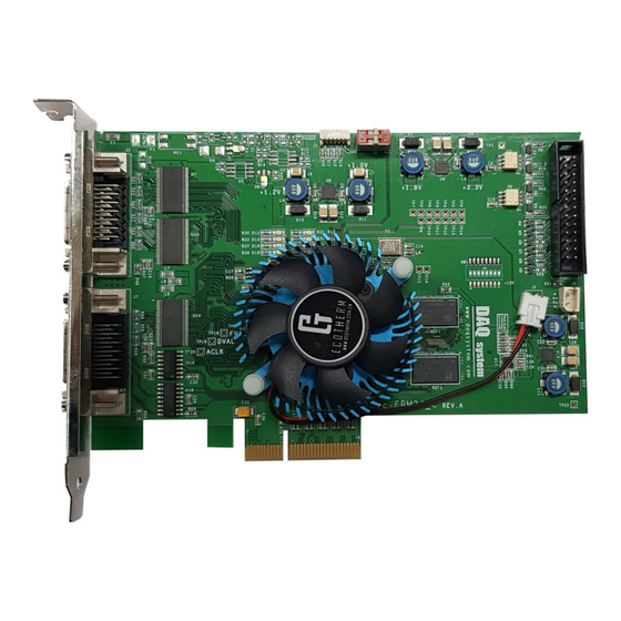
PCIE-FRM24_C User’s Manual 3. PCIE-FRM24_C Board Description Each important board function is briefly described. For detailed function information, please refer to the parts specification. 3-1 PCIE-FRM24_C Board Layout [Figure 3-1. PCIe-FRM24_C Layout] There are several LEDs on the board, and the description of each is as follows. D12 : Blinks when GEN2 is recognized D14 : Blinks when x1 device is recognized D16 : Blinks when x2 device is recognized... -
Page 16: Device Features
PCIE-FRM24_C User’s Manual 3-2 Device Features (1) MDR-26 Connecter : J3, J7 Camera Link Base (J7), medium/Full (J3) Signal Connector (2) LVDS Link : U7, U10, U14 Receive an image frame. (3) FPGA : U13 All of the board functions are controlled by the Logic program of the FPGA. (4) DDR Memory : REF1, REF2 It has 256MB of image buffer memory. -
Page 17: Connector Pin Out
PCIE-FRM24_C User’s Manual 3-3 Connector Pin-out This section describes the connectors and jumpers used in PCIe-FRM24_C. As for main connectors, there are MDR 26pin connectors J3 and J7 connectors for Camera Link connection, and 26pin Box Header connector for external trigger I/O connection. [Figure 3-2] shows the bracket that interfaces with the board and the connection connector. -
Page 18: J1 Connector
PCIE-FRM24_C User’s Manual 3-3-1 J1 Connector J1 is a JTAG (Joint Test Action Group) connector and is used to update the FPGA program on the board. Do not use when operating the board normally. 3-3-2 J2 Switch PCIE-FRM24_C board is designed to use up to 4 PCIe-FRM24_C boards simultaneously in one system (PC). -
Page 19: J3(Mdr) Connector
PCIE-FRM24_C User’s Manual 3-3-3 J3(MDR26) Connector The figure below shows the pin map of the J3 connector of the board used when Medium/Full Configuration Camera Link is used. All pin specifications are input/output based on the Camera Link standard, so please refer to the Camera Link standard document for details. - Page 20 PCIE-FRM24_C User’s Manual [Table 2. J3 Connector] Pin No Name Description Remark Inner Shield Cable shield Z3+- Camera link LVDS receive data11+ ZCLK+ Camera link LVDS receive clock+ Z2+- Camera link LVDS receive data10+ Camera link LVDS receive data9+ Camera link LVDS receive data8+ TERMI- Serial to Camera- Camera link LVDS receive data7 +...
-
Page 21: J4 Connector
PCIE-FRM24_C User’s Manual 3-3-4 J4 Connector J4 is an input/output connector that provides 4 pairs of Isolated Photo-coupler input signals, 4 TTL Inputs, and 2 TTL Output signal lines. [Figure 3-5. J4 Connector (Top View)] [Table 3. J4 PIN-OUT] Name Description N.C. -
Page 22: J5 Connector
PCIE-FRM24_C User’s Manual 3-3-5 J5 Connector (2Pin Header, 2.54mm) It is a 12V FAN power connector. GND/+12V [Figure 3-6. J5 Connector] 3-3-6 J6 Connector 12V external DC power connector. -
Page 23: J7(Mdr) Connector
PCIE-FRM24_C User’s Manual 3-3-7 J7(MDR26) Connector The figure below shows the pin map of the J7 connector of the board used when using the Base Configuration Camera Link. All pin specifications are input/output based on the Camera Link standard, so please refer to the Camera Link standard document for details. Frame Grabber PoCL(+12V) Inner Shield... - Page 24 PCIE-FRM24_C User’s Manual [Table 4. J7 Connector] Pin No Name Description Remark PoCL_Pin Power over Camera Link(+12V) CC4- Camera Control output 4- CC3+ Camera Control output 3+ CC2-- Camera Control output 2- CC1+ Camera Control output 1+ SerTFG+ Serial to Frame grabber + SerTC- Serial to Camera- Camera link LVDS receive data3 +...
-
Page 25: Installation
PCIE-FRM24_C User’s Manual 4. Installation 4-1 Product Contents Before installing the board, check that the contents of the package are intact. PCIe-FRM24_C Board CD (Driver/Manual/API/Sample Source etc.) Document Folder : Manual and Catalog Driver Folder : pcie_frm24.sys, pcie-frm24.inf Sample Folder : Sample Application and DLL TestApp Folder : FrmTest.exe... -
Page 26: Installation Process
PCIE-FRM24_C User’s Manual 4-2 Installation Process The board environment must be Windows 2000 SP4 or higher and Windows XP SP1 or higher. First, turn off the PC's power, plug the PCIe-FRM24 board into the PCI Express Slot, and turn on the PC's power. - Page 27 PCIE-FRM24_C User’s Manual 2. Select Driver from the enclosed CD and click the Next button. 3. Click the Next button. It indicates that the installation process is proceeding as shown below.
- Page 28 PCIE-FRM24_C User’s Manual 4. When the installation is completed normally, it is shown in the figure below. 5. When the installation is complete, check whether the driver is installed normally in the following way. 6. In My Computer -> Properties -> Hardware -> Device Manager, check if the Multifunction Adapter ->...
- Page 29 PCIE-FRM24_C User’s Manual 7. If it appears as shown in the figure below, the installation has been completed normally. The above figure shows the screen where the PCIe-FRM24_C board is normally installed in the PC. (Check the red circle) (Note) After initial installation, the PC must be rebooted for normal operation.
-
Page 30: Sample Program
PCIE-FRM24_C User’s Manual 5. Sample Program DAQ system provides a sample program to make the user be familiar with the board operation and to make the program development easier. You can find the sample program in the CDROM accompanying with the board. One of the execution file is “FrmTest.exe”. It stores the frame data to memory or hard-disk and displays it to Hexa-decimal values which can utilize necessary frame data to developers. - Page 31 PCIE-FRM24_C User’s Manual All files specified above are included on the supplied CDROM. In order to run the sample program normally, the 32/64bit API DLL (pci-frm24c.DLL or pci-frm24c_x64.dll) must be in the folder of the executable file or in the Windows system folder or the folder specified by the Path environment variable.
- Page 32 PCIE-FRM24_C User’s Manual (2) Board # selection It can select a Board #0 ~ Board #3. (Selection J2) (3) “Get Ver.” It shows the version of FPGA and Firmware. (4) “Device Init” button Press this button to initialize the function of receiving image frame data. It is performed only once after power is applied to the board.
- Page 33 PCIE-FRM24_C User’s Manual (8) “Save Data” Press this button, the image begins to save in binary form to the PC. (9) “Close Device” Press this button to finish usage of the board and terminate the program. (10) “Video Data Bits” You can select 8Bit, 16Bit YUV, 24Bit BGR, 8Bit Bayer, 10bit bayer.
-
Page 34: Image Option Function
PCIE-FRM24_C User’s Manual 5-2 Image Option Function (1) “Get Size” It gets the input image resolution of sensor. (2) “Bytes” Select the size of the data width. “1” is 1tap (8bit), “2” is 2Tap (16bit), “4” is 4Tap (32bit), “8” is 8Tap (64bit), and “10” is 10Tap (80bit). Data is transmitted in 64-bit increments from Frame Grabber. - Page 35 PCIE-FRM24_C User’s Manual (6) Mode Selection (Line Scan Camera) “Line Scan”: Toggle to use Line Scan Camera. By default, it is in Area Scan Camera mode. “Page Mode” : You can select Page Mode with Line Scan Camera Option. Continuous --- Use the internal clock 50MHz in Continuous by Free Run Mode. Page Trig --- Use the control signal of the external board.
-
Page 36: Dio Function
PCIE-FRM24_C User’s Manual 5-3 DIO Function (1) “Read I/I” button Read the value of the input port. (2) “On” button Input : When On, Connector J4 Pin17 -> High Output: When On, Connector J4 Pin15 -> High “Off” button Input : When Off, Connector J4 Pin17 -> Low Output: When Off, Connector J4 Pin15 ->... -
Page 37: Cc/Trig Function
PCIE-FRM24_C User’s Manual 5-3 CC/Trig Function You can select GPO_mode or Trigger mode for the CC (Camera Control) signal you want to use. Click the GPO signal below to change from Low to High Active. (1) “GPO_Mode” toggle “GPO Signal”(Checked = High) – CC1 High when checked, Low when unchecked (2) “Trigger Start”... - Page 38 PCIE-FRM24_C User’s Manual Continuous(Free Run) --- Delay, Width, Blank (refer to “Configuration” below. Trigger setting value below) The trigger signal made with the set value is output to CC1. ENC A Trig --- When a rising edge is detected in A-Phase (A-phase), it is output to CC1 as the trigger setting value.
- Page 39 PCIE-FRM24_C User’s Manual Delay Width Blank Trigger Clock Delay Width Blank Trigger Clock Increasing the width increases the width of the pulse. Increasing the Delay and Blank increases the spacing. For example, to use the trigger clock at 5000 hz for CC0 or CC1, use the “CC Cfg” button. Select CC and set Delay / Width / Blank as shown below.
- Page 40 PCIE-FRM24_C User’s Manual (4) Ext Trigger (J4, Pin 21) “On/off” : Trigger Output on/off “Out Signal Inverse” : Invert trigger output “Configuration” : Apply setting value Input Signal Control “ENC A Inverse” : When selected, the waveform of encoder A is inversely converted and input. “ENC B Inverse”...
-
Page 41: Uart Function
PCIE-FRM24_C User’s Manual 5-4 UART Function UART uses two pairs of LVDS (Low Voltage Differential Signals) signals, serial communication, as a communication means between the camera and the frame grabber. It must support at least 9600bps and follow the one start bot, one stop bit, no parity, no handshaking specifications. See [Figure 2-8]. -
Page 42: Grabber Pattern Function
PCIE-FRM24_C User’s Manual 5-6 Grabber Pattern Function (1) “Pclk” Selection Select 60Mhz, 70Mhz, 85Mhz (2) “Data” Selection Select Data 0, Data 1 Pattern output In the case of Data 0, in 4Bytes unit, upper 2bytes is Line Counter, lower 2bytes is Pixel Counter, Pixel Counter increases from 0 to horizontal resolution value, and Line Counter increases from 0 to vertical resolution. - Page 43 PCIE-FRM24_C User’s Manual In the case of Data 1, it is a pixel counter in units of 4 bytes, and the value ranges from 0 to horizontal resolution. When outputting in RGB, it is like the image below. (3) “XRes, YRes” Set horizontal resolution X, vertical resolution Y (4) “Pattern Config, Pattern Off”...
-
Page 44: Set Hsync/De Function
PCIE-FRM24_C User’s Manual 5-7 Set Hsync/DE Function If there is an abnormality in resolution due to an error in Hsync or DE (Data Valid) during the input signal of the camera, there is a problem in the image if there is an error in the resolution. To solve this, Hsync and DE detect the rising edge and forcefully set the desired resolution. -
Page 45: Appendix
PCIE-FRM24_C User’s Manual Appendix Board Size The external sizes of the board are as follows. For detailed dimensions, please contact the person in charge. 139.75 96.5... -
Page 46: Repair Regulations
PCIE-FRM24_C User’s Manual A-2 Repair Regulations Thank you for purchasing a DAQSYSTEM product. Please refer to the following regarding Customer Service regulated by DAQSYSTEM. (1) Read the user manual and follow the instructions before using the DAQSYSTEM product. (2) When returning the product to be repaired, please write down the symptoms of the failure and send it to the head office. -
Page 47: References
-- Camera Link committee 2. PCI Local Bus Specification Revision2.1 -- PCI Special Interest Group 3. How to install PCI DAQ Board -- DAQ system 4. AN201 How to build application using API -- DAQ system 5. AN312 PCIe-FRM24_C API Programming -- DAQ system 6. - Page 48 PCIE-FRM24_C User’s Manual MEMO Contact Point Web sit : https://www.daqsystem.com Email : postmaster@daqsystem.com...
Need help?
Do you have a question about the PCIe-FRM24 C and is the answer not in the manual?
Questions and answers