Table of Contents
Advertisement
Quick Links
PCIe-FRM24
Windows, Windows2000, Windows NT and Windows XP are trademarks of Microsoft. We acknowledge that the
trademarks or service names of all other organizations mentioned in this document as their own property.
Information furnished by DAQ system is believed to be accurate and reliable. However, no responsibility is assumed by DAQ
system for its use, nor for any infringements of patents or other rights of third parties which may result from its use. No license is
granted by implication or otherwise under any patent or copyrights of DAQ system.
The information in this document is subject to change without notice and no part of this document may be copied or
reproduced without the prior written consent.
User's Manual
Copyrights 2005 DAQ system, All rights reserved.
1-
-
PCIe-FRM24 Users Manual (Rev 1.3)
http://www.daqsystem.com
Advertisement
Table of Contents

Related Manuals for DAQ system PCIe-FRM24


Summary of Contents for DAQ system PCIe-FRM24
- Page 1 Information furnished by DAQ system is believed to be accurate and reliable. However, no responsibility is assumed by DAQ system for its use, nor for any infringements of patents or other rights of third parties which may result from its use. No license is granted by implication or otherwise under any patent or copyrights of DAQ system.
-
Page 2: Table Of Contents
PCIe-FRM24 Users Manual (Rev 1.3) -- Contents -- 1. Introduction 2. PCIe-FRM24 Functions 2.1 FPGA Block Diagram 2.2 Encoder Trigger Controller 3. PCIe-FRM24 Board Description 3.1 PCB Layout 3.2 Description of the functional blocks 3.3 Connector Pin-out 3.3.1 J4(MDR26) Connecter 3.3.2 J2(MDR26) Connecter... -
Page 3: Introduction
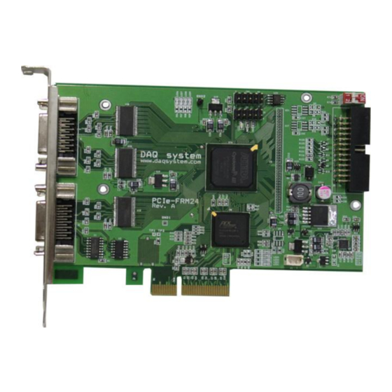
(usually PC). [Figure 1-1. PCIe-FRM24 Board Usage] As shown in Figure [1-1], the PCIe-FRM24 is inserted into any available PCI Express slot in your PC. It receives Image Frame from camera via Camera-Link Standard Interface. And, received data transmit to the API through PCI Express x4 interface. - Page 4 PCIe-FRM24 Users Manual (Rev 1.3) [Figure 1-2. Picture of PCIe-FRM24 board real operation] Figure [1-2] shows physical connection of the board to the Camera-Link Camera. At the left side, there are two Camera-Link connector and received image data (max. 680Mbyte).
- Page 5 PCIe-FRM24 Users Manual (Rev 1.3) [Features of the PCIe-FRM24] Support Base Configuration Camera Link Support Full/Medium Configuration Camera Link Support Line Scan & Area Scan Camera PCI Express 4x Interface Acquisition pixel clock rates up to 85MHz ...
-
Page 6: Pcie-Frm24 Functions
As shown in the following figure, main control of the board is performed in FPGA Core Logic. Primary functions are receiving the image frame data, camera control signal and external Line Trigger I/O. You can control these functions using API provided by DAQ system through PCI Express 4x interface. Local BUS... -
Page 7: Encoder Trigger Controller
PCIe-FRM24 Users Manual (Rev 1.3) 2.2 Encoder Trigger Controller PCIe-FRM24 has 4 pair isolated photo-coupler input signals and 6 TTL level signals for external digital I/O (Motion Controller, Digital I/O board etc.). It can control a camera. [Figure 2-2. Encoder Trigger Control] [Figure 2-3] shows the Photo-coupler circuit. -
Page 8: Pcie-Frm24 Board Description
PCIe-FRM24 Users Manual (Rev 1.3) 3. PCIe-FRM24 Board Description In this chapter, the primary functions of the PCIe-FRM24 board are described briefly. For more information, refer to the device specification 3.1 PCIe-FRM24 Layout [Figure 3-1. PCIe-FRM24 PCB Layout] The board has five LEDs to indicate the operation status. -
Page 9: Description Of The Functional Blocks
PCIe-FRM24 Users Manual (Rev 1.3) 3.2 Description of the functional blocks (1) MDR-26 Connecter : J2, J4 Camera Link Base (J2), medium/Full (J4) Signal Connector (2) LVDS Link : U12, U15, U18 Receive Image frame (3) FPGA : U16 All of the board functions are controlled by the Logic program of the FPGA. -
Page 10: Connector Pin-Out
PCIe-FRM24 Users Manual (Rev 1.3) 3.3 Connecter Pin-out The PCIe-FRM24 board is equipped with MDR 26 Pin connector J2, J4 for Camera Link connection and 26pin Box Header connecter for external Trigger I/O. Figure [3-2] shows the bracket of the board and connector. -
Page 11: J4(Mdr26) Connecter
Camera Link. All of the pin functions are based on the Camera link standard, so please refer to the Camera link standard document for more description and information. Frame Grabber Inner shield Inner shield YCLK- YCLK+ TERMI+ TERMI- ZCLK- ZCLK+ Inner shield Inner shield [Figure 3-3. PCIe-FRM24 J4 Connector Pin-out] http://www.daqsystem.com... - Page 12 PCIe-FRM24 Users Manual (Rev 1.3) [Table 1. J4 Connecter Description] Signal Name Description Remark Cable shield Inner Shield Z3+- Camera link LVDS receive data11+ ZCLK+ Camera link LVDS receive clock+ Z2+- Camera link LVDS receive data10+ Camera link LVDS receive data9+...
-
Page 13: J2(Mdr26) Connecter
Camera link standard document for more description and information. Frame Grabber Inner shield Inner shield Xclk- Xclk+ SerTC+ SerTC- SerTFG- SerTFG+ CC1- CC1+ CC2+ CC2- CC3- CC3+ CC4+ CC4- Inner shield Inner shield [Figure 3-4. PCIe-FRM24 J2 Connector Pin-out] http://www.daqsystem.com... - Page 14 PCIe-FRM24 Users Manual (Rev 1.3) [Table 2. J2 Connecter Description] Signal Name Description Remark Cable shield Inner Shield CC4+- Camera Control output 4+ Refer to Figure 3-5 CC3- Camera Control output 3- Refer to Figure 3-5 CC2+- Camera Control output 2+...
-
Page 15: J1 Connecter
CCx+ Camera Control CCx- Above picture is a Camera Control output circuit from PCIe-FRM24 board to Camera for the specific control of the Camera-link Cable. The PCIe-FRM24 board has four differential digital outputs. Each output is mapped by Digital output. Below picture display that each bit position set. -
Page 16: J7 Connecter
PCIe-FRM24 Users Manual (Rev 1.3) 3.3.5 J7 Connector J7 is an I / O connector that provides four pairs of isolated photo-coupler input signals, four TTL inputs, and two TTL output signal lines.. [Fig 3-5. J7 Connector (Top View)] [Table 3. J7 PIN-OUT Description]... -
Page 17: Sw1
+3.3V Ground 3.3.6 SW1 The PCIe-FRM24 board is designed of four maximum PCIe-FRM24 boards at the same time so as usable. Distribution of each board sets it up through 4 pin switch (SW1) in a board. [Figure 3-6. SW2 Switch] [Table 3. -
Page 18: Installation
In addition to the user‟s Manual, the package includes the following items. If any of these items is missing or damaged, contact DAQ system. After unpacking, inspect the board carton to make sure there are no damages on the board. -
Page 19: Software Driver Installation
To install your PCIe-FRM24 board in your PC, follow the steps described in the document “How to install PCI DAQ Board” provided by DAQ System. If the document is missing, you can get it from www.daqsystem.com. The PCIe-FRM24 board is completely Plug & Play. There are no switches or jumpers to set. - Page 20 PCIe-FRM24 Users Manual (Rev 1.3) Select “Search for the best driver in these locations”. Check “Search removable media (floppy, CD-ROM)”. Check “include this location in the search”. Click “Browse” button. Select the folder where the drivers are located. Click “OK”. Click “Next”.
- Page 21 PCIe-FRM24 Users Manual (Rev 1.3) http://www.daqsystem.com...
- Page 22 Do the following steps to show up the “Device Manager” window. [My Computer -> properties -> Hardware -> Device Manager -> DAQSystem -> PCIe-FRM24] If you can see the “PCIe-FRM24” at Multifunction Adaptors, the driver installation is to have been over. (Check the red circle) Important Notice : After installation, you should re-boot the system for the proper operation.
-
Page 23: Sample Program
PCIe-FRM24 Users Manual (Rev 1.3) 5. Sample Program DAQ system provides a sample program to make the user be familiar with the board operation and to make the program development easier. You can find the sample program in the CDROM accompanying with the board. - Page 24 Another method is to add the directory of API DLL file to PATH environmental variable. Figure [5- 2] is a capture screen to execute “FrameView.exe”. The image that is looked to a monitor as it accesses a Camera-Link connector to PCIe-FRM24 board. Sample program execution sequence is as follows.
-
Page 25: Frameview
PCIe-FRM24 Users Manual (Rev 1.3) (6) ”Half tone” toggle Select Half tone mode. "5th Skip": Skip 5th byte when selected. If Bayer is processed and shown on the screen, the 5th byte is not needed, so use it when removing it. - Page 26 PCIe-FRM24 Users Manual (Rev 1.3) (16) ”Camera Mode” selection 0 : Area 1 : Line (Freerun) 2: Line (Ext) 3: Line (Int) (17) “Save Compare” “Compare” : Compares the original image file with the saved image file and displays the number of bytes incorrectly..
-
Page 27: Appendix
PCIe-FRM24 Users Manual (Rev 1.3) Appendix A.1 General Specification Specification General PCI Express Specification Revision 1.0 PCI Express 4x interface Camera Link interface specification 1.0 and 1.1 Support a Full Camera Link Interface Two 26-pin (MDR-26) Connectors with full support of the “Full”... -
Page 28: Physical Dimension
PCIe-FRM24 Users Manual (Rev 1.3) A.2 Physical Dimension (139.75 x 96.5 mm) 139.75 96.5 http://www.daqsystem.com... - Page 29 PCIe-FRM24 Users Manual (Rev 1.3) References 1. Specification of Camera Link Interface Standard for Digital Cameras and Frame Grabbers -- Camera Link committee 2. PCI Local Bus Specification Revision2.1 -- PCI Special Interest Group 3. How to install PCI DAQ Board -- DAQ system 4.
Need help?
Do you have a question about the PCIe-FRM24 and is the answer not in the manual?
Questions and answers