Table of Contents
Advertisement
Quick Links
PCIe-DIO02
User Manual
Version 1.0
ⓒ 2005 DAQ SYSTEM Co., Ltd. All rights reserved.
Microsoft® is a registered trademark; Windows®, Windows NT®, Windows XP®, Windows 7®, Windows 8®, Windows 10®
All other trademarks or intellectual property mentioned herein belongs to their respective owners.
Information furnished by DAQ SYSTEM is believed to be accurate and reliable, However, no responsibility is assumed by DAQ SYSTEM for its use, nor
for any infringements of patents or other rights of third parties which may result from its use. No license is granted by implication or otherwise under
any patent or copyrights of DAQ SYSTEM.
The information in this document is subject to change without notice and no part of this document may e copied or reproduced without the prior
written consent.
Advertisement
Table of Contents

Subscribe to Our Youtube Channel
Related Manuals for DAQ system PCIe-DIO02


Summary of Contents for DAQ system PCIe-DIO02
- Page 1 All other trademarks or intellectual property mentioned herein belongs to their respective owners. Information furnished by DAQ SYSTEM is believed to be accurate and reliable, However, no responsibility is assumed by DAQ SYSTEM for its use, nor for any infringements of patents or other rights of third parties which may result from its use. No license is granted by implication or otherwise under any patent or copyrights of DAQ SYSTEM.
-
Page 2: Table Of Contents
PCIe-DIO02 User‟s Manual Contents 1. Introduction 1-1 Product Features ------------------------------------------------------------------------ 1-2 Product Applications ------------------------------------------------------------------------ 2. PCI-DIO02 Block Diagram ----------------------------------------------------------- 3. PCI-DIO02 Board Description 3-1 Board Outline ------------------------------------------------------------------------ Device Features ---------------------------------------------------------------------- 4. Connector Pin Map 4-1 VHDCI69 Connector (J2/J3) ---------------------------------------------------------------- J1 Connector... - Page 3 PCIe-DIO02 User‟s Manual 6. Sample Program --------------------------------------------------------------------- 6-1 128bit Digital In Setup ---------------------------------------------------------------------- 6-2 128bit Digital In Setup ---------------------------------------------------------------------- 6-3 128bit Digital In/Out Setup ------------------------------------------------------------------ < Digital Input Terminal Board Circuit Configuration > ----------------------------- < Digital Output Terminal Board Circuit Configuration >...
-
Page 4: Introduction
PCIe-DIO02 User‟s Manual 1. Introduction PCIe-DIO02 is a 128-bit digital input/output board that is perfectly compatible with industrial PCs and uses a PCI Express x1 interface. All control of this board is designed with FPGA (Field Programmable Gate Array), so function enhancement or modification is free, and it can be easily upgraded according to the user's needs. -
Page 5: Product Applications
PCIe-DIO02 User‟s Manual DAQ System Digital I/O Products Product No. In/Out Timer/Counter Specification cPCI-DIO6400 32/32 Isolated Input/Output 128 channels Software cPCI-DIO02 Read/Write in 8 Groups in 16-bit Units Configurable PCI(e)-DIO6400 32/32 Isolated Input/Output PCI-DIO6401 64/None Isolated Input PCI-DIO6402 None/64... -
Page 6: Pci-Dio02 Block Diagram
PCIe-DIO02 User‟s Manual 2. PCIe-DIO02 Block Diagram In the case of PCIe-DIO02, as shown in [Figure 2-1], it has 128 IO ports and is configured to interface with the outside. (Input/Output can be selected and used in the program) It is possible to select Read / Write in 8 groups of 16 bits. -
Page 7: Pci-Dio02 Board Description
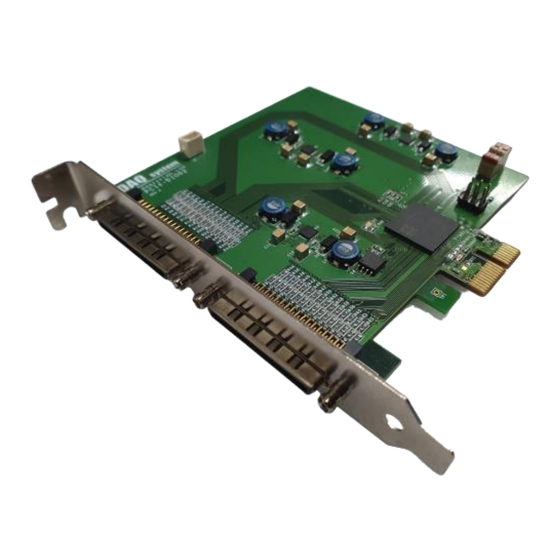
PCIe-DIO02 User‟s Manual 3. PCIe-DIO02 Board Description Each important board function is briefly described. For detailed function information, please refer to the parts specification. 3-1 Board Layout DAQ system www.daqsystem.com PCIe-DIO02 Rev. A PCI Expree x1 Interface [Figure 3-1. PCIe-DIO02 Layout] There are 3 LEDs on the board, and the description of each is as follows. -
Page 8: Device Features
PCIe-DIO02 User‟s Manual 3-2 Device Features (1) VHDCI68 connector: J2, J3 J2 --- External interface (I/O 0~63) J3 --- External interface (I/O 64~127) (2) FPGA : U5 PCI Express signal control and digital I/O functions of the board are controlled through this FPGA Logic. -
Page 9: Connector Pin Map
PCIe-DIO02 User‟s Manual 4. Connector Pin Map This section describes connectors and jumpers used in PCIe-DIO02. As the main connectors, there are VHDCI (Very High Density Cable Interconnect) 68pin connectors J2 and J3 connectors for external digital input/output connection. 4-1 VHDCI68 Connecter (J2, J3) PCIe-DIO02 uses two VHDCI68 connectors for external I/O interface. -
Page 10: J1 Connector
PCIe-DIO02 User‟s Manual 4-2 J1 Connector (2Pin Header, 2.54mm) This is a 12V external DC power connector. Power used when installing CPLD or FPGA, not normally used. 4-3 J4 Connector In a system that requires many I/O ports, if several DIO02 series boards are installed in one system, each board address must be used separately. -
Page 11: Installation
Tighten the screws between the bracket of the board and the connection part of the case. ⑤ In case of multi-board, repeat from step 3. Connect the PCIe-DIO02 board in the PC to an empty PCI slot. When you turn on the power, a new hardware search window will appear. -
Page 12: Driver Installation
PCIe-DIO02 User‟s Manual 5-2 Driver Installation After installing the board, install the driver and sample application to run the board on your PC. For installation, use the supplied CD. The installation procedure is as follows, and unless otherwise specified, it is explained based on Windows XP. - Page 13 PCIe-DIO02 User‟s Manual If new hardware is found, Wizard will ask you to install the corresponding driver. For installation of the driver, select the item “Install from a list or specific location (Advanced)” and click “Next” as in the figure.
- Page 14 PCIe-DIO02 User‟s Manual If the installation is completely finished, you can show below message window.
- Page 15 If you can see the “PCI-DIO02” at Multifunction Adaptors, the driver installation is to have been over. The PCIe-DIO02 board is compatible with the PCI-DIO02 board driver and is expressed as PCI- DIO02 using the same driver. (Check the red circle)
-
Page 16: Sample Program
PCIe-DIO02 User‟s Manual 6. Sample Program In the APP folder of the CDROM provided with the board, a sample program "PCI_DIO02.exe" is provided for easy use of the board. In order to test the sample program, the board driver must be installed first. - Page 17 PCIe-DIO02 User‟s Manual (1) „Model No‟ Button It selects the motel name PCI-DIO02. (2) „Board No‟ Button It selects the selected board number (Board # 0 ~ Board # 3) when clicked. The board number can be set to SW1 in the board and connect up to 4 units.
-
Page 18: 128Bit Digital In Setup
PCIe-DIO02 User‟s Manual 1111 1111 1111 1111 1111 1111 1111 1110 (FFFE) 1111 1111 1111 1101 (FFFD) 1111 1111 1111 1011 (FFFB) 1111 1111 1111 0111 (FFF7) 1011 1111 1111 1111 (BFFF) 0111 1111 1111 1111 (7FFF) . Check with „Read All‟ or „Auto DIN Read‟ check. Check with „Read All‟ or „Auto DIN Read‟... - Page 19 PCIe-DIO02 User‟s Manual [Figure 6-3] shows the connection method using the ACC-DIO_B_INPUT terminal board and the ACC-DIO_E_INPUT terminal board. [Figure 6-3. 128bit Digital In Connection]...
-
Page 20: 128Bit Digital In Setup
PCIe-DIO02 User‟s Manual 6-2 128bit Digital Out Setup When using all 128 bits as output, the sample program settings are as follows. [Figure 6-4. Sample Program 128bit Digital Out Screen]... - Page 21 PCIe-DIO02 User‟s Manual [Figure 6-5] shows the connection method using the ACC-DIO_B_OUTPUT terminal board and the ACC-DIO_E_OUTPUT terminal board. [Figure 6-5. 128bit Digital Out Connection]...
-
Page 22: 128Bit Digital In/Out Setup
PCIe-DIO02 User‟s Manual 6.3 128bit Digital In/Out Setup When 128 bits are used as 64 bits of input and output, the sample program settings are as follows. [Figure 6-6. Sample Program 128bit Digital In/Out Screen] [Figure 6-7] shows the connection method using the ACC-DIO_B_INPUT and ACC-DIO_E_INPUT boards and the ACC-DIO_B_OUTPUT and ACC-DIO_E_OUTPUT boards. - Page 23 PCIe-DIO02 User‟s Manual [Figure 6-7. 128bit Digital In/Out Connection]...
- Page 24 PCIe-DIO02 User‟s Manual In case of using ACC-DIO_B board and ACC-DIO_E board that have 16-bit input/output board together, the sample program setting is as follows. [Figure 6-8. Sample Program 128bit Digital In/Out Screen]...
- Page 25 PCIe-DIO02 User‟s Manual [Figure 6-9] shows the connection method using the ACC-DIO_B terminal board and the ACC- DIO_E terminal board. [Figure 6-9. 128bit Digital In/Out Connection]...
-
Page 26: Digital Input Terminal Board Circuit Configuration
PCIe-DIO02 User‟s Manual < Digital Input Terminal Board Circuit Configuration > Terminal Board PCI-DIO02 3.3V ACC-DIO_B_INPUT VHDCI Conn. ACC-DIO_E_INPUT IN_COM0 2.4K DIN0 3.3V 2.4K DIN1 3.3V 2.4K DIN7 In the figure above, the digital input circuit is isolated by a port coupler. When a positive voltage is applied to the "IN_COM"... - Page 27 PCIe-DIO02 User‟s Manual...
-
Page 28: Digital Output Terminal Board Circuit Configuration
PCIe-DIO02 User‟s Manual Digital Output Terminal Board Circuit Configuration > < Terminal Board PCI-DIO02 ACC-DIO_B_OUTPUT VHDCI Conn ACC-DIO_E_OUTPUT OUT_COM OUT_POWER (5V) DOUT0 out0 OUT_POWER (5V) out1 DOUT1 OUT_POWER (5V) out7 DOUT7 In the figure, the digital output circuit is isolated by a port coupler. "OUT_POWER" and "OUT_VDD"... - Page 29 PCIe-DIO02 User‟s Manual...
-
Page 30: Digital Input/Output Terminal Board Circuit Configuration
PCIe-DIO02 User‟s Manual Digital Input/Output Terminal Board Circuit Configuration > < There are two IN-COMs on the terminal board ACC-DIO_B for every eight photocouplers. In addition, there are OUT-COM for every 8 photo couplers, and there are 2 OUT-COM. That is, you can use a 16-bit input/output board with one board. -
Page 31: Appendix
PCIe-DIO02 User‟s Manual Appendix A-1 Repair Regulations Thank you for purchasing DAQSYSTEM's product. Please refer to the following regarding Customer Service stipulated by DAQSYSTEM. Please read the user's manual and follow the instructions before using the DAQSYSTEM product. When returning the product to be repaired, please send it to the head office with the symptoms of the malfunction as well. - Page 32 PCIe-DIO02 User‟s Manual References 1. PCI System Architecture -- MindShare Inc. 2. PCI Local Bus Specification -- PCI-SIG 3. AN201 How to build application using APIs -- DAQ system 4. AN242 PCI-DIO02 API Programming -- DAQ system...
- Page 33 PCIe-DIO02 User‟s Manual MEMO Contact Point Web sit : https://www.daqsystem.com Email : postmaster@daqsystem.com...
Need help?
Do you have a question about the PCIe-DIO02 and is the answer not in the manual?
Questions and answers