Table of Contents
Advertisement
Quick Links
PCIe-FRM11
Windows, Windows2000, Windows NT and Windows XP are trademarks of Microsoft. We acknowledge that the
trademarks or service names of all other organizations mentioned in this document as their own property.
Information furnished by DAQ system is believed to be accurate and reliable. However, no responsibility is assumed by DAQ
system for its use, nor for any infringements of patents or other rights of third parties which may result from its use. No license is
granted by implication or otherwise under any patent or copyrights of DAQ system.
The information in this document is subject to change without notice and no part of this document may be copied or
reproduced without the prior written consent.
User's Manual
Copyrights 2008 DAQ system, All rights reserved.
1
-
-
PCIe-FRM11 User's Manual (Rev 1.4)
http://www.daqsystem.com
Advertisement
Table of Contents

Subscribe to Our Youtube Channel
Related Manuals for DAQ system PCIe-FRM11


Summary of Contents for DAQ system PCIe-FRM11
- Page 1 Information furnished by DAQ system is believed to be accurate and reliable. However, no responsibility is assumed by DAQ system for its use, nor for any infringements of patents or other rights of third parties which may result from its use. No license is granted by implication or otherwise under any patent or copyrights of DAQ system.
-
Page 2: Table Of Contents
PCIe-FRM11 User’s Manual (Rev 1.4) -- Contents -- 1. Introduction 2. PCIe-FRM11 Functions 3. PCIe-FRM11 Board Description 3.1 PCB Layout 3.2 Description of the functional blocks 3.3 Connector Pin-out 4. Installation 4.1 Package content 4.2 Installation Sequence 5. Sample Program 5.1 FrmTest Program... -
Page 3: Introduction
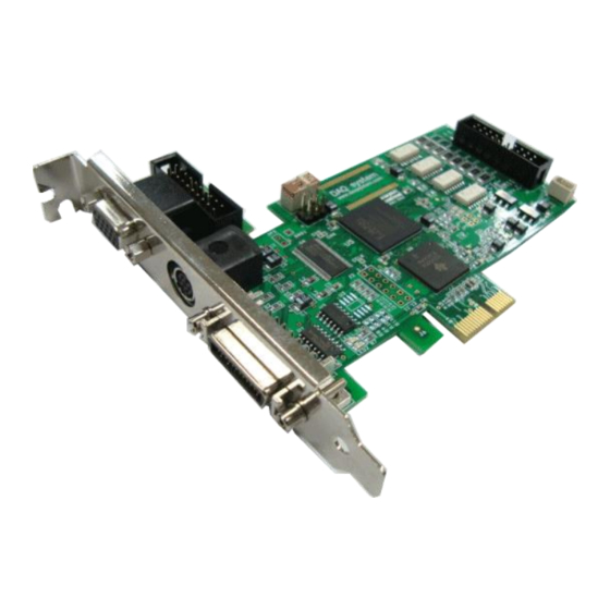
(usually PC). [Figure 1-1. PCIe-FRM11 board Usage] As shown in Figure [1-1], the PCIe-FRM11 is inserted into any available PCI Express slot in your PC. It receives Image Frame from camera via Camera-Link Standard Interface. And, received data transmit to the API through PCI Express x1 interface. - Page 4 PCIe-FRM11 User’s Manual (Rev 1.4) [Figure 1-2. Picture of PCIe-FRM11 board] Figure [1-2] shows physical connection of the board to the Camera-Link Camera. At the left side, there are 15 pin D-SUB connector and 26 pin MDR connector. The former is for connection to external I/O device, and the other is for connection to Camera-link camera for frame data or UART communication.
- Page 5 PCIe-FRM11 User’s Manual (Rev 1.4) [Features of the PCIe-FRM11 board] Base Configuration Camera Link Interface CC1/CC2 Trigger PCI Express 1x interface PCI Bus Master Operation Receiving 24/16/8bit Frame data UART Tx/Rx (8 bit data, 1 start, 1 stop, No parity, 9600bps) ...
-
Page 6: Pcie-Frm11 Functions
PCIe-FRM11 User’s Manual (Rev 1.4) 2. PCIe-FRM11 Functions As shown in the following figure, main control of the board is performed in FPGA Core Logic. Primary functions are receiving the image frame data, transmitting/receiving UART data and controlling 8 bit digital inputs, and 8 bit digital outputs. However, it supports 5 bit digital inputs and 8 bit digital outputs for external interface with Dsub15 port. - Page 7 Control) signals. All 11 LVDS signal lines, including two LVDS lines, are transmitted over the MDR cable. The transmitted signal is deserialized through the Channel Link chip in the PCIe-FRM11 into four image LVDS serial signals into a 28-bit parallel video signal and control signals (Frame Valid, Line...
- Page 8 The above picture shows the camera control output circuit that can send the control signal from the PCIe-FRM11 board to the camera via the camera-link cable. All four digital outputs are output through Differential method. Each output is mapped to a digital output and output. Each bit position is shown in [Figure 2-3] below.
-
Page 9: Pcie-Frm11 Board Description
PCIe-FRM11 User’s Manual (Rev 1.4) 3. PCIe-FRM11 Board Description In this chapter, the primary functions of the PCIe-FRM11 board are described briefly. For more information, refer to the device specification. 3.1 PCB Layout [Figure 3-1. PCIe-FRM11 PCB Layout] The board has five LEDs to indicate the operation status. -
Page 10: Description Of The Functional Blocks
PCIe-FRM11 User’s Manual (Rev 1.4) 3.2 Description of the functional blocks (1) U1 : Differential Line Receiver Camera Control Signal (CC1 ~ CC4). [See Figure 2-3.] (2) U2 : I2C Serial EEPROM U6 PCI Express Chipset Configuration (3) U3 : Differential Line Driver/Receiver Serial Communication between Camera and Frame Grabber. -
Page 11: Connector Pin-Out
PCIe-FRM11 User’s Manual (Rev 1.4) 3.3 Connector Pin-out The PCIe-FRM11 board is equipped with MDR 26 Pin connector J1 for Camera Link connection and D-SUB 15 Pin connector J2 for external I/O connection and Mini-Circular connector for external power supply. - Page 12 CC1- CC1+ CC2+ CC2- CC3- CC3+ CC4+ CC4- Inner shield Inner shield [Figure 3-3. PCIe-FRM11 J1 Connector Pin-out] [Table 1. J1 Connector Description] Pin# Signal Name Description Remark Inner Shield Cable shield CC4- Camera Control output 4- Refer to Figure 4-4...
- Page 13 PCIe-FRM11 User’s Manual (Rev 1.4) Camera link LVDS receive clock + Xclk+ Camera link LVDS receive data2 + Camera link LVDS receive data1 + Camera link LVDS receive data0 + Inner Shield Inner Shield CC4+ Camera Control output 4+ Refer to Figure 4-4...
- Page 14 PCIe-FRM11 User’s Manual (Rev 1.4) [Description of J5 connector] PCIe-FRM11 Board has six photo-coupler isolated digital inputs and four equivalent outputs. Each is available from J5 connector. The equivalent circuit is as shown Figure [3-5]. 2.4K DINx IN_COM < Photo coupler input>...
- Page 15 PCIe-FRM11 User’s Manual (Rev 1.4) [Table 2. J5 Connector Description] Pin# Signal Name Description Remark DIN0 Input 0 DIN4 Input 4 DIN1 Input 1 DIN5 Input 5 DIN2 Input 2 DIN6 Input 6 DIN3 Input 3 DIN7 Input 7 DIN_COM...
- Page 16 PCIe-FRM11 User’s Manual (Rev 1.4) [Description of D-Sub15 connector] The PCIe-FRM11 board has five digital inputs isolated by a photo-coupler, and eight digital outputs can be connected to the D-Sub15 connector on the board via a J5 connector. The pin map of the Dsub- 15 connector is shown below.
- Page 17 PCIe-FRM11 User’s Manual (Rev 1.4) [Photo-coupler Digital Input] [Figure 3-8. Photo-coupler Digital Input circuit] Photo-coupler inputs are routed from connector P1 (DSUB 15Pin), each inputs are matched with DIO input bit position from 4 to 0 as shown in Figure [3-8].
- Page 18 PCIe-FRM11 User’s Manual (Rev 1.4) [Photo-coupler Digital Output] [Figure 3-9. Photo-coupler Digital Output Circuit] Photo-coupler outputs are routed to connector P1 (DSUB 15PIN), each outputs are matched with DIO output bit position from 7 to 0 as shown in Figure [3-9].
- Page 19 PCIe-FRM11 User’s Manual (Rev 1.4) [Description of Mini-Circular connector] PCIe-FRM11 has a six pin mini-circular connector to supply DC12 for external camera. Maximum current is 1A, but need another power supply in case of over 1A. [Figure 3-10. Mini-Circular Connector pin-out] [Table 4.
- Page 20 PCIe-FRM11 User’s Manual (Rev 1.4) [Description of SW1] PCIe-FRM11 board is designed of four maximum PCIe-FRM11 boards at the same time so as usable. Distribution of each board sets it up through 4 pin switch (SW1) in a board. [Figure 3-11. SW1 pin-out] [Table 5.
-
Page 21: Installation
To install your PCIe-FRM11 board in your PC, follow the steps described in the document “How to install PCI DAQ Board” provided by DAQ System. If the document is missing, you can get it from www.daqsystem.com. The PCIe-FRM11 board is completely Plug & Play. There are no switches or jumpers to set. - Page 22 PCIe-FRM11 User’s Manual (Rev 1.4) click “Next” as in the figure. http://www.daqsystem.com...
- Page 23 PCIe-FRM11 User’s Manual (Rev 1.4) If the installation is completely finished, you confirm it in the following ways. Do the following steps to show up the “Device Manager” window. [My Computer -> properties -> Hardware -> Device Manager -> Multifunction Adaptors ->...
- Page 24 PCIe-FRM11 User’s Manual (Rev 1.4) [Figure 4-2. “System Properties” window-“Hardware” Tab] http://www.daqsystem.com...
- Page 25 PCIe-FRM11 User’s Manual (Rev 1.4) [Figure 4-3. “Device Manager” window] If you can see the “PCIe-FRM11” at Multifunction Adaptors, the driver installation is to have been over. (Check the red circle) Important Notice : After installation, you should re-boot the system for the proper operation.
-
Page 26: Sample Program
PCIe-FRM11 User’s Manual (Rev 1.4) 5. Sample Program DAQ system provides a sample program to make the user be familiar with the board operation and to make the program development easier. You can find the sample program in the CDROM accompanying with the board. -
Page 27: Functions Related To Image Frame
PCIe-FRM11 User’s Manual (Rev 1.4) To run the sample application program, you need to use API, it is a form of client DLL. To compile the sample source to make its executable file, you have to use Import Library files and header files. - Page 28 PCIe-FRM11 User’s Manual (Rev 1.4) (8) „FRAME Read‟ button Press this button to read the image frame data of the board to your PC. If image frame data is not saved on the board, you must wait until the end of data collection.
-
Page 29: Functions Related To Dio
PCIe-FRM11 User’s Manual (Rev 1.4) (13) „Frame View‟ button When you click, the screen displays only once. (14) „Auto View‟ click When you click, the screen shows video. (15) „R_B Swap‟ click Converts the color of the image. (Red <-> Blue) (16) „Auto Save‟... -
Page 30: Functions Related To Cc
Transmits data to the UART. After writing the data to be transferred in the editor box, press the button (4) „Get Data‟ button The UART data transmitted from the camera to the PCIe-FRM11 is read. (5) „Hex Display‟ selection Show UART data as Hex value. - Page 31 PCIe-FRM11 User’s Manual (Rev 1.4) When the default setting Delay / Width / Blank is set to 0/0/0, it is output as 16.6Mhz because it is 60ns (15 + 45) in total. When the setting value increases by 1 as shown in the figure below, The value is increased by 15 ns.
- Page 32 PCIe-FRM11 User’s Manual (Rev 1.4) Trigger Clock 45us 154.5us (4) „Inv. CC„ button Inverts the pulse of the selected CC1 or CC2 Trigger. Normal Invert http://www.daqsystem.com...
-
Page 33: Frm11_Test Program
PCIe-FRM11 User’s Manual (Rev 1.4) 5.2 FRM11_TEST [Figure 5-3. When Sample program “FRM11_TEST.exe” is executed] This programs sets the DVAL or HVAL for valid data line. DVAL Use : DVAL(Data Valid) Use HVAL Use : HVAL(Frame Valid) Use http://www.daqsystem.com... -
Page 34: Test
PC in this figure, but actually it is located in a PCI slot inside the PC. The image frame data is generated in the Image Frame Simulator made by DAQ System. If you have real camera or a frame source, you can use it. -
Page 35: Uart Tx/Rx Test
“Save to” button. It saves the contents of the editor box to a file. 6.2 UART Tx/Rx Test At the above stage, make the image frame simulator to send UART data to PCIe-FRM11 board periodically. Step 1 : Press the “UART init” button to initialize the UART and then press the “Start Timer” to get the UART data from the Image Frame Simulator. -
Page 36: Appendix
PCIe-FRM11 User’s Manual (Rev 1.4) Appendix A.1 General Specification Specification General PCI Local Bus Specification Revis ion 1.0 PCI Express 1x Interface PCI Target and Master operation Camera Link interface specification +5V Single Power operation , Max 300mA under Interface ... -
Page 37: Physical Dimension
PCIe-FRM11 User’s Manual (Rev 1.4) A.2 Physical Dimension 120.8 http://www.daqsystem.com... - Page 38 PCIe-FRM11 User’s Manual (Rev 1.4) References 1. Specification of Camera Link Interface Standard for Digital Cameras and Frame Grabbers -- Camera Link committee 2. PCI Local Bus Specification Revision2.1 -- PCI Special Interest Group 3. How to install PCI DAQ Board -- DAQ system 4.
Need help?
Do you have a question about the PCIe-FRM11 and is the answer not in the manual?
Questions and answers