Table of Contents
Advertisement
Quick Links
www.ti.com
User's Guide
ADS1x48EVM Evaluation Module
The ADS1x48 evaluation module (EVM) allows users to evaluate the functionality of the Texas Instruments'
16-bit ADS1148 or the 24-bit ADS1248. ADS1x48 refers to what is common to both devices and EVMs.
Any differences in operation between the devices or EVMs are listed separately. The ADS1x48 devices are
highly integrated delta-sigma ADCs that include a programmable gain amplifier, a 2.048-V voltage reference,
an internal oscillator, dual current sources (IDACs), and several system-monitoring features. Each ADS1x48
device has inputs that can be configured as seven single-ended or four differential inputs. All of these features
integrated into the ADS1x48 devices enable precision measurement for many types of analog temperature
sensors including thermocouples, resistance temperature detectors (RTDs), and thermistors. This user's guide
describes both the EVM hardware platform and the graphical user interface (GUI) software used to configure
and operate the device. This user's guide also includes the EVM schematic diagram, board layout, and bill
of materials. The EVM platform eases the evaluation of the ADS1x48 device with hardware, software, and
computer connectivity through the universal serial bus (USB) interface.
Throughout this document, the abbreviation EVM and the term evaluation module are synonymous with the
ADS1x48EVM.
SBAU378A – SEPTEMBER 2021 – REVISED JANUARY 2022
Submit Document Feedback
ABSTRACT
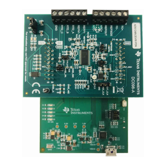
ADS1x48 Evaluation Module (ADS1248EVM Shown)
Copyright © 2022 Texas Instruments Incorporated
ADS1x48EVM Evaluation Module
1
Advertisement
Table of Contents

Related Manuals for Texas Instruments ADS1x48EVM


Summary of Contents for Texas Instruments ADS1x48EVM
- Page 1 ADS1x48EVM Evaluation Module ABSTRACT The ADS1x48 evaluation module (EVM) allows users to evaluate the functionality of the Texas Instruments' 16-bit ADS1148 or the 24-bit ADS1248. ADS1x48 refers to what is common to both devices and EVMs. Any differences in operation between the devices or EVMs are listed separately. The ADS1x48 devices are highly integrated delta-sigma ADCs that include a programmable gain amplifier, a 2.048-V voltage reference,...
-
Page 2: Table Of Contents
Table of Contents www.ti.com Table of Contents Introduction.....................................5 2 Getting Started With the ADS1x48EVM..........................3 ADS1x48EVM Overview................................. 3.1 Analog and Digital Power Supplies............................ 3.2 Voltage Reference Options..............................3.3 Clock Options...................................10 3.4 Digital Interface.................................11 3.5 Analog Input Connections..............................4 ADS1x48EVM GUI................................. - Page 3 Figure 3-1. LED Indicators D1 and D5............................7 Figure 3-2. Jumper (JP1) Selects AVDD on the ADS1x48EVM....................Figure 3-3. ADS1x48EVM VREF Options (Yellow) and Test Points (Red).................. Figure 3-4. ADC Clock Options on the ADS1x48EVM......................Figure 3-5. ADS1x48EVM-to-PAMBoard Connections......................Figure 3-6. ADS1x48EVM Analog Input Terminal Blocks (J5, Left; J6, Right)................12...
- Page 4 Table 1-1. Related Documentation.............................. Table 3-1. Summary of ADS1x48EVM VREF Options.........................9 Table 3-2. ADS1x48EVM Header Pinout and Description......................Table 3-3. ADS1x48EVM Terminal Block Input Description (J5 and J6)..................12 Table 3-4. ADS1x48EVM Terminal Block (J6) to ADC Connections..................17 Table 3-5. ADS1x48EVM Settings for Different RTD Types......................
-
Page 5: Introduction
The ADS1x48EVM requires an external controller to evaluate the ADS1x48 device. The PAMBoard is controlled by commands received from the ADS1x48EVM GUI, and returns data to the GUI for display and analysis. If the PAMBoard is not used, the EVM plug-in module format allows for an alternative external host to communicate with the ADS1x48 through the pin headers J1 through J4. -
Page 6: Getting Started With The Ads1X48Evm
2 Getting Started With the ADS1x48EVM The following list of steps provides an overview to quickly get the ADS1x48EVM setup and operational. The subsequent sections in this document expand on each step in order to explain in detail the available features on the ADS1x48EVM and the corresponding GUI. -
Page 7: Ads1X48Evm Overview
The ADS1x48 supports a wide unipolar analog supply voltage (AVDD) range from 2.7 V to 5.5 V and a bipolar AVDD of ±2.5 V. The ADS1x48EVM AVDD can be set to either 3.3 V or 5 V. Power is supplied from the USB 5-V source to the PAMBoard. -
Page 8: Figure 3-2. Jumper (Jp1) Selects Avdd On The Ads1X48Evm
JP1 is made. The ADS1x48 devices accept a digital supply voltage (DVDD) range from 2.7 V to 5.25 V. On the ADS1x48EVM, the ADS1x48 DVDD is a fixed value of 3.3 V. As with AVDD, this 3.3-V DVDD is sourced from the USB power-supply voltage and is used as the PAMBoard DVDD. -
Page 9: Voltage Reference Options
The ADS1x48 also has two sets of differential VREF inputs defined as REFP0, REFN0 and REFP1, REFN1. All of these options are selected via the MUX1 register in the ADS1x48. The ADS1x48EVM supports four different VREF options to offer maximum flexibility. Table 3-1 details these four options. -
Page 10: Clock Options
ADS1x48 offers an external CLK input pin if an external clock signal is required. Choose between these flexible clock options using the JP2 header on the ADS1x48EVM. Enable the internal oscillator by connecting the shunt to the JP2-3 pin on the JP2 header. This pin is marked... -
Page 11: Digital Interface
Section 3.1, the PAMBoard operates at a 3.3-V logic level provided by the host computer and the ADS1x48EVM board uses this same 3.3-V logic level for DVDD. Digital interface connections from the ADS1x48EVM to the PAMBoard include power, I C, SPI, and a GPIO connection used to trigger an interrupt at the end of conversion that signifies new data are available. -
Page 12: Analog Input Connections
3.5 Analog Input Connections The ADS1x48EVM is designed for easy interface to external temperature sensors using the two screw terminal blocks (J5 and J6). Connector J5 provides connections for thermocouples and thermistors as well as the 2.048-V output voltage from the ADS1x48 integrated reference and the dedicated 2.5-V output from the REF5025. -
Page 13: Figure 3-7. Thermocouple Input Structure On The
Although thermocouples are self-powered, these components must be biased in order to avoid floating beyond the input range of the PGA integrated into the ADC. The ADS1x48EVM offers multiple ways to bias the thermocouple so that the output voltage can be successfully read by the ADC. - Page 14 This document also discusses the need for cold junction compensation (CJC), which is used in conjunction with the thermocouple voltage to derive the measured temperature. The ADS1x48EVM includes provisions for a CJC measurement using a thermistor, which is discussed in more detail in the next section.
-
Page 15: Figure 3-9. Thermistor Input Structure On The Ads1X48Evm
1.93 kHz. Additionally, each input has a common-mode filter with a cutoff frequency of 38.63 kHz. NTC+ and NTC– are connected through the filter resistors to two analog inputs (AIN6 and AIN7, respectively) on the ADS1x48. Figure 3-9 shows the portion of the ADS1x48EVM schematic with J5 and the thermistor input structure. NTC+ AIN6 4.12k... -
Page 16: Figure 3-11. Pcb Layout For J5 Terminal Block Showing Copper Pours For Cjc Measurement
Figure 3-9, thermistor RT1 is not populated by default on the ADS1x48EVM. Choose a 10-kΩ NTC thermistor in a 0603 package for this component. To measure the thermistor voltage, follow the steps outlined at the end of Section 3.5.2, noting that step #1 (connect the... -
Page 17: Figure 3-12. Rtd Input Structure On The Ads1X48Evm
ADS1x48EVM Overview 3.5.3 Connecting an RTD to J6 on the ADS1x48EVM The RTD input connections on J6 are J6:3, J6:4, and J6:5, which correspond to the RTD_A, RTD_B, and RTD_C nets, respectively. Additionally, terminal block J6 provides a pair of differential reference inputs, REFP1 and REFN1, which correspond to inputs J6:1 and J6:2, respectively. - Page 18 IDAC routing. The following subsections detail the appropriate connections and settings to enable each RTD configuration using the ADS1x48EVM. Each subsection contains a connection diagram where the red lines indicate how current flows in the circuit. Moreover, the red text indicates which jumpers are populated and which current sources are biasing the RTD, and the blue text indicates the measurement channels.
-
Page 19: Figure 3-13. Connection Diagram For A 2-Wire Rtd Using A Low-Side R
ADS1x48EVM Overview 3.5.3.1 Connecting a 2-Wire RTD Using a Low-Side R to J6 on the ADS1x48EVM Figure 3-13 shows how to connect a 2-wire RTD using a low-side R configuration to J6. IDA C AIN1 REFP1 REFP1 REFN1 REFN1... -
Page 20: Figure 3-14. Connection Diagram For A 2-Wire Rtd Using A High-Side R
ADS1x48EVM Overview www.ti.com 3.5.3.2 Connecting a 2-Wire RTD Using a High-Side R to J6 on the ADS1x48EVM Figure 3-14 shows how to connect a 2-wire RTD using a high-side R configuration to J6. IDA C AIN1 REFP1 REFP1 REFN1 REFN1... -
Page 21: Figure 3-15. Connection Diagram For A 3-Wire Rtd Using One Idac And A Low-Side R
ADS1x48EVM Overview 3.5.3.3 Connecting a 3-Wire RTD Using One IDAC and a Low-Side R to J6 on the ADS1x48EVM Figure 3-15 shows how to connect a 3-wire RTD using one IDAC and a low-side R configuration to J6. IDA C... -
Page 22: Figure 3-16. Connection Diagram For A 3-Wire Rtd Using One Idac And A High-Side R
ADS1x48EVM Overview www.ti.com 3.5.3.4 Connecting a 3-Wire RTD Using One IDAC and a High-Side R to J6 on the ADS1x48EVM Figure 3-16 shows how to connect a 3-wire RTD using one IDAC and a high-side R configuration to J6. IDA C... -
Page 23: Figure 3-17. Connection Diagram For A 3-Wire Rtd Using Two Idacs And A Low-Side R
ADS1x48EVM Overview 3.5.3.5 Connecting a 3-Wire RTD Using Two IDACs and a Low-Side R to J6 on the ADS1x48EVM Figure 3-17 shows how to connect a 3-wire RTD using two IDACs and a low-side R configuration to J6. IDA C... -
Page 24: Figure 3-18. Connection Diagram For A 3-Wire Rtd Using Two Idacs And A High-Side R
ADS1x48EVM Overview www.ti.com 3.5.3.6 Connecting a 3-Wire RTD Using Two IDACs and a High-Side R to J6 on the ADS1x48EVM Figure 3-18 shows how to connect a 3-wire RTD using two IDACs and a high-side R configuration to J6. IDA C... -
Page 25: Figure 3-19. Connection Diagram For A 4-Wire Rtd Using A Low-Side R
ADS1x48EVM Overview 3.5.3.7 Connecting a 4-Wire RTD Using a Low-Side R to J6 on the ADS1x48EVM Figure 3-19 shows how to connect a 4-wire RTD using a low-side R configuration to J6. IDA C AIN1 REFP1 REFP1 REFN1 REFN1... -
Page 26: Figure 3-20. Connection Diagram For A 4-Wire Rtd Using A High-Side R
3.5.3.9 Summary of ADS1x48EVM RTD Configuration Settings Table 3-5 summarizes the required IDAC, jumper, and analog input channel settings to measure each RTD configuration using the ADS1x48EVM. Table 3-5. ADS1x48EVM Settings for Different RTD Types No. of IDACs IDAC Channels AINP... -
Page 27: Figure 3-21. Using The Tc± Inputs On J5 As General-Purpose Signal
3.5.4 Connecting a General-Purpose Input to J5 on the ADS1x48EVM Although the ADS1x48EVM is designed for measuring all types of analog temperature sensors, general-purpose input signals can be applied to the ADS1x48 through the TC± inputs on the J5 terminal block. -
Page 28: Ads1X48Evm Gui
3. Refresh the GUI such that a green signal displays and the Hardware Connected indicator shows in the bottom status ribbon (see Figure 4-2). Figure 4-1. Browser Extension and TI Cloud Agent Installation When connected, the ADS1x48EVM GUI has multiple pages to help navigate and control the ADS1x48EVM: • Home • Data Capture •... -
Page 29: Figure 4-2. Ads1X48Evm Gui Home Page
One other important feature of the Home page is an information icon next to the device name. Clicking the icon, as shown in Figure 4-3, displays specific information regarding the ADS1x48EVM. Figure 4-3. Connected Hardware Information SBAU378A – SEPTEMBER 2021 – REVISED JANUARY 2022... -
Page 30: Figure 4-4. File Menu
About displays specific information regarding the GUI and EVM hardware to help confirm that the latest version of the GUI is being used ADS1x48EVM Evaluation Module SBAU378A – SEPTEMBER 2021 – REVISED JANUARY 2022 Submit Document Feedback Copyright © 2022 Texas Instruments Incorporated... -
Page 31: Data Capture
The number of samples cannot be changed while data are being collected. SBAU378A – SEPTEMBER 2021 – REVISED JANUARY 2022 ADS1x48EVM Evaluation Module Submit Document Feedback Copyright © 2022 Texas Instruments Incorporated... -
Page 32: Figure 4-7. Capture Statistics
GUI below the statistics. Figure 4-8 shows the Time Domain plot and its features. Figure 4-8. Time Domain Plot ADS1x48EVM Evaluation Module SBAU378A – SEPTEMBER 2021 – REVISED JANUARY 2022 Submit Document Feedback Copyright © 2022 Texas Instruments Incorporated... -
Page 33: Register Map
Throughout the Register Map window question mark icons appear. Clicking on these icons provides details pertaining to the items in the locations where they appear. See Figure 4-10 for more details. SBAU378A – SEPTEMBER 2021 – REVISED JANUARY 2022 ADS1x48EVM Evaluation Module Submit Document Feedback Copyright © 2022 Texas Instruments Incorporated... -
Page 34: Figure 4-10. Register Map
Immediately Write operation on the Config register when options change. All read and write options are discussed in more detail in the next sections. Figure 4-11. Register Read and Write Controls ADS1x48EVM Evaluation Module SBAU378A – SEPTEMBER 2021 – REVISED JANUARY 2022 Submit Document Feedback Copyright © 2022 Texas Instruments Incorporated... -
Page 35: Figure 4-12. Auto Read Options
ADS1x48 registers. The advantage of manually reading the register contents is reduced USB communication between the ADS1x48EVM and the GUI. The registers can be read automatically from the ADS1x48 at a variety of intervals from once per second to as fast as possible. -
Page 36: Bill Of Materials, Printed Circuit Board Layout, And Schematic
Bill of Materials, Printed Circuit Board Layout, and Schematic www.ti.com 5 Bill of Materials, Printed Circuit Board Layout, and Schematic This section contains the ADS1x48EVM bill of materials (BOM), printed-circuit board (PCB) layout, and board schematic. 5.1 Bill of Materials Table 5-1 lists the bill of materials (BOM) for the ADS1x48EVM. - Page 37 RES, 10.0 M, 1%, 0.1 W, CRCW060310M0FKEA Vishay-Dale AEC-Q200 Grade 0, 0603 Thermistor NTC, 10k ohm, ERT-J1VR103H Panasonic 3%, 0603 SBAU378A – SEPTEMBER 2021 – REVISED JANUARY 2022 ADS1x48EVM Evaluation Module Submit Document Feedback Copyright © 2022 Texas Instruments Incorporated...
-
Page 38: Printed Circuit Board Layout
5.2 Printed Circuit Board Layout Figure 5-1 Figure 5-7 depict the ADS1x48EVM PCB layout. Red = top layer; blue = bottom layer; yellow = top silkscreen; internal GND layers not shown Figure 5-1. Composite PCB Layout ADS1x48EVM Evaluation Module SBAU378A –... -
Page 39: Figure 5-2. Top Silkscreen
Figure 5-2. Top Silkscreen Figure 5-3. Top Layer Figure 5-4. Internal Ground Layer 1 Figure 5-5. Internal Ground Layer 2 SBAU378A – SEPTEMBER 2021 – REVISED JANUARY 2022 ADS1x48EVM Evaluation Module Submit Document Feedback Copyright © 2022 Texas Instruments Incorporated... -
Page 40: Figure 5-6. Bottom Layer
Bill of Materials, Printed Circuit Board Layout, and Schematic www.ti.com Figure 5-6. Bottom Layer Figure 5-7. Bottom Silkscreen ADS1x48EVM Evaluation Module SBAU378A – SEPTEMBER 2021 – REVISED JANUARY 2022 Submit Document Feedback Copyright © 2022 Texas Instruments Incorporated... -
Page 41: Schematic
RTD_A RTD_B RTD_C IEXC2 REF5025IDGKT RTD_A AIN2 4.12k 1000pF 0.01uF RTD_B 1000pF AIN3 4.12k RTD_C IEXC1 Figure 5-8. ADS1x48EVM Schematic SBAU378A – SEPTEMBER 2021 – REVISED JANUARY 2022 ADS1x48EVM Evaluation Module Submit Document Feedback Copyright © 2022 Texas Instruments Incorporated... -
Page 42: Revision History
Revision A (January 2022)) Page • Deleted inclusive terminology from document....................• Changed EVM landing page links to correct locations throughout document............ ADS1x48EVM Evaluation Module SBAU378A – SEPTEMBER 2021 – REVISED JANUARY 2022 Submit Document Feedback Copyright © 2022 Texas Instruments Incorporated... - Page 43 STANDARD TERMS FOR EVALUATION MODULES Delivery: TI delivers TI evaluation boards, kits, or modules, including any accompanying demonstration software, components, and/or documentation which may be provided together or separately (collectively, an “EVM” or “EVMs”) to the User (“User”) in accordance with the terms set forth herein.
- Page 44 www.ti.com Regulatory Notices: 3.1 United States 3.1.1 Notice applicable to EVMs not FCC-Approved: FCC NOTICE: This kit is designed to allow product developers to evaluate electronic components, circuitry, or software associated with the kit to determine whether to incorporate such items in a finished product and software developers to write software applications for use with the end product.
- Page 45 www.ti.com Concernant les EVMs avec antennes détachables Conformément à la réglementation d'Industrie Canada, le présent émetteur radio peut fonctionner avec une antenne d'un type et d'un gain maximal (ou inférieur) approuvé pour l'émetteur par Industrie Canada. Dans le but de réduire les risques de brouillage radioélectrique à...
- Page 46 www.ti.com EVM Use Restrictions and Warnings: 4.1 EVMS ARE NOT FOR USE IN FUNCTIONAL SAFETY AND/OR SAFETY CRITICAL EVALUATIONS, INCLUDING BUT NOT LIMITED TO EVALUATIONS OF LIFE SUPPORT APPLICATIONS. 4.2 User must read and apply the user guide and other available documentation provided by TI regarding the EVM prior to handling or using the EVM, including without limitation any warning or restriction notices.
- Page 47 Notwithstanding the foregoing, any judgment may be enforced in any United States or foreign court, and TI may seek injunctive relief in any United States or foreign court. Mailing Address: Texas Instruments, Post Office Box 655303, Dallas, Texas 75265 Copyright © 2019, Texas Instruments Incorporated...
- Page 48 TI products. TI’s provision of these resources does not expand or otherwise alter TI’s applicable warranties or warranty disclaimers for TI products. TI objects to and rejects any additional or different terms you may have proposed. IMPORTANT NOTICE Mailing Address: Texas Instruments, Post Office Box 655303, Dallas, Texas 75265 Copyright © 2022, Texas Instruments Incorporated...
Need help?
Do you have a question about the ADS1x48EVM and is the answer not in the manual?
Questions and answers