
Related Manuals for Texas Instruments ADS1224EVM


Summary of Contents for Texas Instruments ADS1224EVM
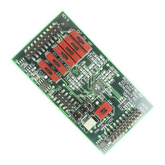
- Page 1 ADS1224EVM Evaluation Module User’s Guide Data Acquisition Products April 2004 SBAU095...
- Page 2 TI product or service and is an unfair and deceptive business practice. TI is not responsible or liable for any such statements. Following are URLs where you can obtain information on other Texas Instruments products and application solutions:...
- Page 3 EVM IMPORTANT NOTICE Texas Instruments (TI) provides the enclosed product(s) under the following conditions: This evaluation kit being sold by TI is intended for use for ENGINEERING DEVELOPMENT OR EVALUATION PURPOSES ONLY and is not considered by TI to be fit for commercial use. As such, the goods being provided may not be complete in terms of required design-, marketing-, and/or manufacturing-related protective considerations, including product safety measures typically found in the end product incorporating the goods.
- Page 4 EVM schematic located in the EVM User’s Guide. When placing measurement probes near these devices during operation, please be aware that these devices may be very warm to the touch. Mailing Address: Texas Instruments Post Office Box 655303 Dallas, Texas 75265 Copyright 2004, Texas Instruments Incorporated...
- Page 5 Preface Read This First About This Manual This manual describes the ADS1224EVM evaluation fixture and how to use it. Throughout this document, the abbreviation EVM and the term evaluation module are synonymous with the ADS1224EVM. Information About Cautions and Warnings This book contains cautions.
- Page 6 Related Documentation From Texas Instruments The following documents provide information regarding Texas Instruments in- tegrated circuits used in the assembly of the ADS1224EVM. These docu- ments are available from the TI web site. The last character of the literature number corresponds to the document revision, which is current at the time of the writing of this User’s Guide.
-
Page 7: Table Of Contents
Contents Contents Overview ............... . Introduction . - Page 8 Contents Figures 2−1. Connectors and Jumpers ............2−2.
-
Page 9: Overview
Chapter 1 Overview The ADS1224EVM is an evaluation fixture for the ADS1224 24-bit delta-sigma (∆Σ) analog-to-digital converter (ADC). The ADS1224EVM is designed for prototyping and evaluation. Topic Page Introduction .......... -
Page 10: Introduction
The ADS1224EVM is designed using a standard card format developed by TI. This simple, consistent design makes the ADS1224EVM very easy to connect to your own prototype system. You can even think of the ADS1224EVM as an alternate package for the ADS1224—one much larger than the device itself, but also much easier to wire up by hand on your test bench. -
Page 11: Built-In Accessories
Built-in Accessories 1.2 Built-in Accessories The ADS1224EVM includes a system clock oscillator and a low-noise voltage reference. Both of these components are optional; you can select an external system clock and an external reference using slide switches. The +2.5V voltage reference is derived from a Burr-Brown REF1004-2.5, which is buffered by an OPA350 and filtered by a capacitor. -
Page 12: Controls
1.5 Setting Up The ADS1224EVM is configured according to its use. Thus, there is no single correct procedure to follow in order configure the test fixture. Nevertheless, it is useful to remember the following things when you are set- ting up the board: Make certain that the digital supply level is correct. - Page 13 Setting Up Check the system clock switch. If it is set to EXT, and you have not con- nected a clock signal to the external clock input pin on J2, the ADS1224 will not operate. The ADS1224 has several configuration input pins connected to pins on J2.
- Page 14 Setting Up...
-
Page 15: Circuit Description
Chapter 2 Circuit Description This chapter describes the connectors, controls, and circuit design of the ADS1224EVM in detail. Topic Page I/O Connectors and Testpoints ....... . . -
Page 16: I/O Connectors And Testpoints
I/O Connectors and Testpoints 2.1 I/O Connectors and Testpoints The positions and functions of the connectors and testpoints are shown in Figure 2−1. Figure 2−1. Connectors and Jumpers ANALOG SERIAL CONNECTOR CONNECTOR POWER JUMPER CONNECTOR BLOCK Many of the pins on the connectors are not used. On the pinout diagrams, un- used pins are not marked. - Page 17 J1: Analog Connector 2.1.1 J1: Analog Connector The analog connector pinout is shown in Figure 2−2 and described in Table 2−1. Figure 2−2. Analog Connector Pinout AN0− AN0+ AN1− AN1+ AN2− AN2+ AN3− AN3+ AGND AGND AGND OBREF AGND REF− AGND REF+ Although certain pins are described as “negative,”...
- Page 18 J1: Analog Connector Table 2−1. Analog Connector Pin Descriptions Pin Number Pin Name Standard Direction Function Connection Name AN0− AN0− Input Through S1 Negative input 0 AN0+ AN0+ Input Through S2 Positive input 0 AN1− AN1− Input Through S3 Negative input 1 AN1+ AN1+ Input...
-
Page 19: J2: Serial Connector
J2: Serial Connector 2.1.2 J2: Serial Connector The serial connector pinout diagram is shown in Figure 2−3 and described in Table 2−2. Figure 2−3. Serial Connector Pinout TEMPSEN MUX0 SCLK DGND MUX1 DGND DOUT DRDY EXTCLK DGND BUFEN Table 2−2. Serial Connector Pin Descriptions Pin Number Pin Name Standard Name... -
Page 20: J3: Power Connector
Positive Digital Supply, +5V Digital supply, selected using J4 Note: The ADS1224EVM has a single ground domain. The ground is always connected to DGND. It may also be connected to AGND using J4 pins 11−12. The ADS1224 uses an analog supply of +5V and a digital supply of +1.8V to +5.5V. -
Page 21: Jumpers
Jumpers 2.2 Jumpers There are six jumper positions on the ADS1224EVM. All are contained in jumper block J4. The pinout of this jumper block is shown in Figure 2−5. Figure 2−5. Jumper Block ADCAVDD AVDD DVDD +1.8VD DVDD +3.3VD DVDD... -
Page 22: J4 Pins 5−10: Digital Power Supply Select
Connect only one of pin pairs 5−6, 7−8 or 9−10. Shorting more than one of these jumpers can potentially damage your motherboard, or even damage the ADS1224EVM itself. The ADS1224 inputs are not 5V tolerant, nor are they TTL-compatible. Although protection resistance is included in each digital line, it may be neces- sary to provide level translation if the ADS1224 digital supply must be powered from a different voltage than the external logic. -
Page 23: Switches
Switches 2.3 Switches The positions and functions of the EVM switches are shown in Figure 2−6. Figure 2−6. Switches CH 1 INPUT S1, S2 SWITCHES CH 2 INPUT S3, S4 SWITCHES CLOCK VREF INPUT SELECT S5, S6 SWITCHES 2.3.1 S1−4: Input Select Switches These switches control which lines are routed to the ADS1224 channel 0 (AIN0) and channel 1 (AIN1) inputs. - Page 24 Switches Since the switches for both the negative and positive inputs for each channel have the same configuration, it is easy to set up the inputs for a variety of applications. Some examples are given in Table 2−5. Table 2−5. Common Input Switch Settings Setting S1/3 S2/4...
-
Page 25: S5−6: Reference Select
Switches 2.3.2 S5−6: Reference Select These two switches control which signals are applied to the ADS1224 differen- tial reference input pins. The positions of the switches are described in Table 2−6 and Table 2−7. Some common combinations of S5 and S6 are shown in Table 2−8. Table 2−6. -
Page 26: S5: System Clock Select
2.3.3 S5: System Clock Select This switch selects which of the two available clock sources on the ADS1224EVM will be provided to the ADS1224. The positions of the switch are described in Table 2−9. Table 2−9. System Clock Select Switch... -
Page 27: Usage
Chapter 3 Usage This chapter provides guidelines on using the ADS1224EVM and connecting other systems to it. Topic Page Input Filtering Capacitors ........ -
Page 28: Input Filtering
Input Filtering 3.1 Input Filtering Each channel pair on the ADS1224EVM has pads for a differential RC filter, as shown in Figure 3−1. Figure 3−1. Channel Input Filter OUTPUT INPUT TO ADC As shipped, the resistor pads are populated with 0Ω resistors, and the capaci- tor pads are unpopulated. -
Page 29: Serial Interface
3.4 Clock Circuitry The ADS1224 does not have a built-in clock oscillator, and requires an external clock signal in order to operate. The ADS1224EVM has a 4MHz clock oscilla- tor chip on board to supply the clock signal. In some cases, it is desirable to operate the ADS1224 at a different frequency. - Page 30 Clock Circuitry...
-
Page 31: Schematic And Layout
This chapter contains the complete bill of materials, schematic diagram, and printed circuit board (PCB) layout for the ADS1224EVM. Note: Board layouts are not to scale. They are intended to show how the board is laid out; they are not intended to be used for manufacturing ADS1224EVM PCBs. Topic Page Schematic . -
Page 32: Schematic
Schematic 4.1 Schematic Figure 4−1. Schematic... -
Page 33: Printed Circuit Board Layout
Printed Circuit Board Layout 4.2 Printed Circuit Board Layout The ADS1224EVM is a four-layer PCB. The layer stack order, from top to bottom, is component (top) layer, ground plane, power plane, and solder (bottom) layer. Four layers were necessary to accommodate the many components on the board. -
Page 34: Bill Of Materials
1µF ceramic chip capacitor, Murata GRM188R61A105KA61D ±10%, X5R, 0603, 10V 22µF ceramic chip capacitor, Murata GRM31CR60J226KE19L ±10%, X5R, 6.3V Analog-to-digital converter Texas Instruments ADS1224IPW Operational amplifier Texas Instruments OPA350UA Voltage reference, 2.5V Texas Instruments REF1004I−2.5 EEPROM, 1 C, 256K bits...
Need help?
Do you have a question about the ADS1224EVM and is the answer not in the manual?
Questions and answers