Table of Contents
Advertisement
Quick Links
To our customers,
st
On April 1
, 2010, NEC Electronics Corporation merged with Renesas Technology
Corporation, and Renesas Electronics Corporation took over all the business of both
companies. Therefore, although the old company name remains in this document, it is a valid
Renesas Electronics document. We appreciate your understanding.
Issued by: Renesas Electronics Corporation (http://www.renesas.com)
Send any inquiries to http://www.renesas.com/inquiry.
Old Company Name in Catalogs and Other Documents
Renesas Electronics website:
http://www.renesas.com
st
April 1
, 2010
Renesas Electronics Corporation
Advertisement
Table of Contents

Related Manuals for Renesas M3A-HS64

Summary of Contents for Renesas M3A-HS64
- Page 1 On April 1 , 2010, NEC Electronics Corporation merged with Renesas Technology Corporation, and Renesas Electronics Corporation took over all the business of both companies. Therefore, although the old company name remains in this document, it is a valid Renesas Electronics document. We appreciate your understanding.
- Page 2 Renesas Electronics. Renesas Electronics shall not be in any way liable for any damages or losses incurred by you or third parties arising from the use of any Renesas Electronics product for an application categorized as “Specific”...
- Page 3 SH7264 CPU Board M3A-HS64 User's Manual Renesas 32-bit RISC Microcomputer SuperH RISC engine Family/SH7260 Series Rev.1.00 2009.04...
- Page 4 Please be sure to implement safety measures to guard against the possibility of physical injury, and injury or damage caused by fire in the event of the failure of a Renesas product, such as safety design for hardware and software including but not limited to redundancy, fire control and malfunction prevention, appropriate treatment for aging degradation or any other applicable measures.
- Page 5 As a result, this equipment, including all accessories, must not be disposed of as household waste but through your locally recognised recycling or disposal schemes. As part of our commitment to environmental responsibility Renesas also offers to take back the equipment and has implemented a Tools Product Recycling Program for customers in Europe.
- Page 6 This page is blank for reasons of layout.
-
Page 7: Table Of Contents
2.2.1 SH7264 Overview ............................. 2-3 2.2.2 SH7264 Pin Functions Used on the M3A-HS64....................2-3 2.2.3 M3A-HS64 Module Availability .......................... 2-9 2.2.4 SH7264 Multiplex Pins Used on the M3A-HS64 ..................... 2-10 2.3 Memory ..................................2-12 2.3.1 SH7264 Internal RAM ............................. 2-12 2.3.2 NOR Flash Memory Interface.......................... - Page 8 2.10 Power Supply Module............................. 2-27 2.11 E10A-USB Interface ............................... 2-28 Chapter 3 M3A-HS64G01 Functions ....................3-1 3.1 Overview of Functions ..............................3-2 3.2 CPU.................................... 3-3 3.2.1 SH7264 Overview ............................. 3-3 3.2.2 SH7264 Pin Functions Used on the M3A-HS64G01 ..................3-3 3.2.3 M3A-HS64G01 Module Availability ........................
- Page 9 Chapter 5 M3A-HS64 Operating Specifications .................. 5-1 5.1 M3A-HS64 Connectors............................... 5-2 5.1.1 USB Connectors (J1 and J2)..........................5-4 5.1.2 H-UDI Connector (36-pin, J3)..........................5-6 5.1.3 5 V Power Supply Connector (J4) ........................5-7 5.1.4 5 V Input AC Adapter Jack (J6)......................... 5-8 5.1.5 H-UDI Connector (14-pin, J7)..........................
- Page 10 7.2.2 Switches and LEDs ............................7-28 7.3 M3A-HS64G02 Dimensions ............................. 7-29 Appendix..............................A-1 SCHEMATICS (iv) Rev. 1.00 Apr 30, 2009 REJ11J0034-0100...
-
Page 11: Chapter 1Overview
Chapter 1Overview Chapter 1 Overview... -
Page 12: Introduction
1.1.1 SH7264 CPU board (Part number: M3A-HS64) The M3A-HS64 comes standard with 4-MB NOR flash memory (16-bit bus width), 16-MB SDRAM (16-bit bus width), 256-MB NAND flash memory (16-bit bus width) and 2-MB serial flash memory as its external memory. The M3A-HS64 has three boot options;... -
Page 13: M3A-Hs64 Configuration
Overview 1.2 M3A-HS64 Configuration 1.2 M3A-HS64 Configuration The following figure shows an example of the system configuration using the M3A-HS64. Figure 1.2.1 M3A-HS64 System Configuration Example Rev. 1.00 Apr 30, 2009 REJ11J0034-0100... -
Page 14: M3A-Hs64 Board Specifications
Overview 1.3 M3A-HS64 Board Specifications 1.3 M3A-HS64 Board Specifications Table 1.3.1 and Table 1.3.2 describe the board specifications of the M3A-HS64. Table 1.3.1 Board Specifications (1/2) Item Description • SH7264 Input (XIN) clock: 18 MHz Bus clock: 72 MHz at maximum... - Page 15 Overview 1.3 M3A-HS64 Board Specifications Table 1.3.2 Board Specifications (2/2) Item Description • Dimensions: 148 mm x 105 mm • Mounting form: 6 layers, double-sided Board specifications • Board thickness: 1.6 mm • Number of boards: 1 Rev. 1.00 Apr 30, 2009...
-
Page 16: M3A-Hs64 Exterior
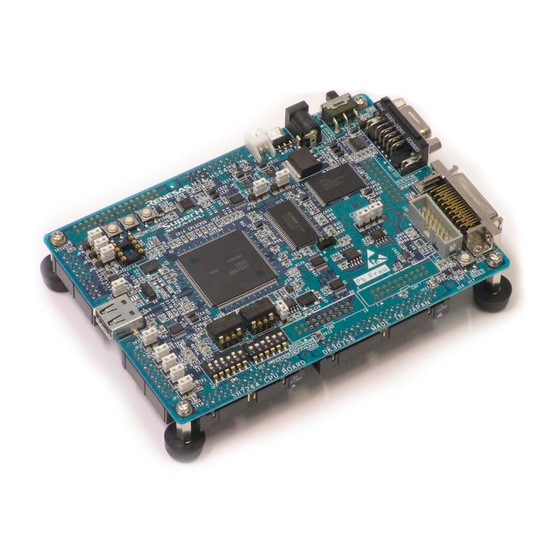
Overview 1.4 M3A-HS64 Exterior 1.4 M3A-HS64 Exterior The following figure shows the exterior of the M3A-HS64. Figure 1.4.1 SH7264 CPU board Exterior Rev. 1.00 Apr 30, 2009 REJ11J0034-0100... -
Page 17: M3A-Hs64 Block Diagram
Overview 1.5 M3A-HS64 Block Diagram 1.5 M3A-HS64 Block Diagram The following figure shows the system block diagram of the M3A-HS64. H-UDI connector RS-232C connector (36-/14-pin) H-UDI SCIF Switches (Interrupt, DIP switches) INTC EEPROM EEPROM IIC3 (16 KB) (16 KB) VBUS... -
Page 18: M3A-Hs64 Major Components
1.6 M3A-HS64 Major Components 1.6 M3A-HS64 Major Components Figure 1.6.1 and Figure 1.6.2 show the M3A-HS64 layout and locations of the major components (PCB drawing). Figure 1.6.1 M3A-HS64 Component Layout and Placement (Top View of the Component Side) Rev. 1.00 Apr 30, 2009... - Page 19 Overview 1.6 M3A-HS64 Major Components Figure 1.6.2 M3A-HS64 Layout and Component Placement (Top View of the Solder Side) Rev. 1.00 Apr 30, 2009 REJ11J0034-0100...
- Page 20 Overview 1.6 M3A-HS64 Major Components The following tables list the major components on the M3A-HS64. Table 1.6.1 Major components on the M3A-HS64 - ICs (1/3) Name Part Number Manufacturer Name Remarks board R5S72643P144FPU Renesas Main MCU SDRAM EDS1216AHTA-75E ELPIDA 16-bit bus, 16 MB...
-
Page 21: M3A-Hs64G01 Configuration
The following figure shows an example of the system configuration using the M3A-HS64G01 (optional board for audio). IEBus UART Optional board for audio M3A-HS64G01 SH7264 CPU board M3A-HS64 SD card 12 V DC output regulated power supply (3A min.) RSPDIF... -
Page 22: M3A-Hs64G01 Board Specifications
• Includes a card power control IC (Software control NOT allowed) CAN (Controller Area Network) communication by the SH7264 on-chip CAN (RCAN-TL1) • HA13721FP (Renesas CAN driver IC), includes a voltage level shifter IEBus communication by the SH7264 on-chip IEBus controller (IEB) IEBus •... -
Page 23: M3A-Hs64G01 Exterior
Overview 1.9 M3A-HS64G01 Exterior 1.9 M3A-HS64G01 Exterior The following figure shows the exterior of the M3A-HS64G01. Figure 1.9.1 M3A-HS64G01 Exterior Rev. 1.00 Apr 30, 2009 1-13 REJ11J0034-0100... -
Page 24: M3A-Hs64G01 Block Diagram
Overview 1.10 M3A-HS64G01 Block Diagram 1.10 M3A-HS64G01 Block Diagram The following figure shows the block diagram of the M3A-HS64G01. Bluetooth Power control SD card SCIF Interface connector SDHI AK4524 Character Line-out RSPI DAC/ADC Mic-in SSIF AK4353 Optical IIC3 connector LCD module VDC3 Interface Line-out... -
Page 25: M3A-Hs64G01 Major Components
Overview 1.11 M3A-HS64G01 Major Components 1.11 M3A-HS64G01 Major Components Figure 1.11.1 and Figure 1.11.2 show the M3A-HS64G01 layout and locations of the major components (PCB drawing). Figure 1.11.1 M3A-HS64G01 Layout and Component Placement (Top View of the Component Side) Rev. 1.00 Apr 30, 2009 1-15 REJ11J0034-0100... - Page 26 Overview 1.11 M3A-HS64G01 Major Components Figure 1.11.2 M3A-HS64G01 Layout and Component Placement (Top View of the Solder Side) Rev. 1.00 Apr 30, 2009 1-16 REJ11J0034-0100...
- Page 27 SUNLIKE 16 characters x 2 lines Audio codec AK4524VF 24-bit 96 kHz audio codec D/A converters AK4353VF 96 kHz 24-bit D/A converter CAN drivers HA13721FP Renesas IEBus driver HA12187FP Renesas Adjustable regulator LTC3727EG 8 V/5 V Multiplexers SN74CB3Q3257DBQR Analog switch Table 1.11.2 Major Components -Connectors (2)
-
Page 28: M3A-Hs64G02 Configuration
The following figure shows an example of the system configuration using the M3A-HS64G02 (optional board for graphic display). IEBus UART Optional board for graphic display M3A-HS64G02 SH7264 CPU board M3A-HS64 SD card 12 V DC output regulated Timer power supply output (3A min.) -
Page 29: M3A-Hs64G02 Board Specifications
SD card interface • Includes a card power control IC (Software control NOT allowed) CAN communication by the SH7264 on-chip CAN (RCAN-TL1) • HA13721FP (Renesas CAN driver IC), includes a voltage level shifter IEBus communication by the SH7264 on-chip IEBus controller (IEB) IEBus •... -
Page 30: M3A-Hs64G02 Exterior
Overview 1.14 M3A-HS64G02 Exterior 1.14 M3A-HS64G02 Exterior The following figure shows the exterior of the M3A-HS64G02. Figure 1.14.1 M3A-HS64G02 Exterior Rev. 1.00 Apr 30, 2009 1-20 REJ11J0034-0100... -
Page 31: M3A-Hs64G02 Block Diagram
Overview 1.15 M3A-HS64G02 Block Diagram 1.15 M3A-HS64G02 Block Diagram The following figure shows the block diagram of the M3A-HS64G02. Power control SD card UART SCIF connector Interface SDHI Interface AK4353 Optical connector IIC3 LCD module Interface Line-out SSIF AK8851 VDC3 Video Video In decoder... -
Page 32: M3A-Hs64G02 Major Components
Overview 1.16 M3A-HS64G02 Major Components 1.16 M3A-HS64G02 Major Components The following figure shows the M3A-HS64G02 layout and locations of the major components (PCB drawing). Figure 1.16.1 M3A-HS64G02 Layout and Component Placement (Top View of the Component Side) Rev. 1.00 Apr 30, 2009 1-22 REJ11J0034-0100... - Page 33 Overview 1.16 M3A-HS64G02 Major Components Figure 1.16.2 M3A-HS64G02 Layout and Component Placement (Top View of the Solder Side) Rev. 1.00 Apr 30, 2009 1-23 REJ11J0034-0100...
- Page 34 SD1602H SUNLIKE 16 characters x 2 lines Video decoder AK8851VQ Supports NTSC/PAL/ SECAM D/A converter AK4353VF 96 kHz, 24-bit D/A converter CAN drivers HA13721FP Renesas IEBus driver HA12187FP Renesas Adjustable regulator LTC3727EG 8 V/5 V Multiplexers SN74CB3Q3257DBQR Analog switch Table 1.16.2 Major Components -Connectors (2/2)
-
Page 35: Memory Maps
Overview 1.17Memory Maps 1.17 Memory Maps The following figure shows memory map examples of the SH7264 and the M3A-HS64. M3A-HS64 Logic address SH7264 logic space Memory Map H'0000 0000 Flash memory (4 MB) 16-bit bus CS0 space: 64 MB H'0040 0000... -
Page 36: Absolute Maximum Ratings
Overview 1.18 Absolute Maximum Ratings 1.18 Absolute Maximum Ratings Table 1.18.1 and Table 1.18.2 list the absolute maximum ratings of the M3A-HS64, and its optional boards. Table 1.18.1 Absolute Maximum Ratings on the M3A-HS64 Symbol Parameter Value Remarks 5 V system power supply voltage -0.3 to 6.0 V... -
Page 37: Usage Note
Overview 1.20 Usage Note 1.20 Usage Note This section describes usage note the SH7264 CPU board and optional boards. 1.20.1 Configuring Unused Pins Set the SH7264 unused (unconnected) multiplexed pins to output when not connecting the optional board with the SH7264 CPU board. - Page 38 Overview 1.20 Usage Note This page intentionally left blank. Rev. 1.00 Apr 30, 2009 1-28 REJ11J0034-0100...
-
Page 39: Chapter 2 M3A-Hs64 Functions
Chapter 2 M3A-HS64 Functions Chapter 2 M3A-HS64 Functions... -
Page 40: Overview Of Functions
M3A-HS64 Functions 2.1 Overview of Functions 2.1 Overview of Functions M3A-HS64 includes the function modules listed in the following table. Table 2.1.1 M3A-HS64 Function Modules Section Function Description • SH7264 • Connects the SH7264 external bus interface and an NOR flash memory... -
Page 41: Cpu
2.2 CPU 2.2.1 SH7264 Overview The M3A-HS64 includes the SH7264, the 32-bit RISC MCU that operates with a maximum frequency of 144 MHz. 2.2.2 SH7264 Pin Functions Used on the M3A-HS64 Table 2.2.1 to Table 2.2.6 list the SH7264 pin functions used on the M3A-HS64. - Page 42 M3A-HS64 Functions 2.2.2 SH7264 Pin Functions Used on the M3A-HS64 Table 2.2.2 SH7264 Pin Functions (2/6) Expansion Description Remarks Name Symbol connector PB16/A16/TIOC4A Address bus CN4, pin 20 CKIO CKIO Connected to the SDRAM CLK pin CN6, pin 20 PVcc...
- Page 43 M3A-HS64 Functions 2.2.2 SH7264 Pin Functions Used on the M3A-HS64 Table 2.2.3 SH7264 Pin Functions (3/6) Expansion Description Remarks Name Symbol connector PVcc Connects the USB external clock to USB_X1 USB_X1 48 MHz USB_X2 USB_X2 Open ASEMD# ASEMD# ASE mode select...
- Page 44 M3A-HS64 Functions 2.2.2 SH7264 Pin Functions Used on the M3A-HS64 Table 2.2.4 SH7264 Pin Functions (4/6) Expansion Description Remarks Name Symbol connector PG16/LCD_VSYNC/TIOC1A/ CN9, pin 19 TxD3/CTS1# PG15/LCD_DATA15/TIOC0D/ CN9, pin 20 RxD3/RTS1# PG14/LCD_DATA14/TIOC0C/ CN9, pin 17 SCK1 PG13/LCD_DATA13/TIOC0B/ CN9, pin 18...
- Page 45 M3A-HS64 Functions 2.2.2 SH7264 Pin Functions Used on the M3A-HS64 Table 2.2.5 SH7264 Pin Functions (5/6) Expansion Name Symbol Description Remarks connector SW5-5: ON RSPCK0 Connected to the serial flash memory SCK pin SW5-6: OFF PF9/A23/SSISCK3/RSPCK0/ SW5-5: OFF CN7, pin 30...
- Page 46 M3A-HS64 Functions 2.2.2 SH7264 Pin Functions Used on the M3A-HS64 Table 2.2.6 SH7264 Pin Functions (6/6) Expansion Description Remarks Name Function connector PD14/D14/NAF6/PWM2G D14/NAF6 Data bus CN8, pin 3 PD13/D13/NAF5/PWM2F D13/NAF5 Data bus CN8, pin 6 PD12/D12/NAF4/PWM2E D12/NAF4 Data bus...
-
Page 47: M3A-Hs64 Module Availability
Y: Yes N: No Notes: 1: When using LED2, and LED3, SW5-1, SW5-2, and SW5-3 on the M3A-HS64 cannot be used. 2: PF9, and PF10 are multiplex pins. When setting SW5-5, and SW5-6, either serial or NAND can be used. -
Page 48: Sh7264 Multiplex Pins Used On The M3A-Hs64
2.2.4 SH7264 Multiplex Pins Used on the M3A-HS64 Table 2.2.8 to Table 2.2.14 list SH7264 multiplex pin functions used on the M3A-HS64. These multiplex pins are set as port input pins by default. Set the MD bit in the port control register to use the SH7264 peripheral functions (except I/O ports). - Page 49 M3A-HS64 Functions 2.2.4 SH7264 Multiplex Pins Used on the M3A-HS64 Table 2.2.12 SH7264 Multiplex Pin Functions (FLCTL) Peripheral SH7264 Port Control Register SH7264 Pin Name Multiplex Pin Name Function Register Name MD bit Setting FLCTL NAF7 PDCR3 PD15MD[1:0] = B'01...
-
Page 50: Memory
2.3.2 NOR Flash Memory Interface The M3A-HS64 comes standard with an NOR flash memory listed in the table below to store the user program. The NOR flash memory works at 16-bit mode, and 3.3 V-only single power supply. It is write-protected or write-enabled by system setting DIP switches. - Page 51 M3A-HS64 Functions 2.3.2 NOR Flash Memory Interface Table 2.3.2 DIP Switches Setting (SW6-1) Function Number OFF (High) ON (Low) SW6-1 NOR flash memory is write-enabled (default) NOR flash memory is write-protected The figure below shows the write and read access timing example of the NOR flash memory. The table below lists the bus state controller settings (write/read) when the SH7264 bus clock works at 72 MHz.
-
Page 52: External Sdram Interface
2.3.3 External SDRAM Interface 2.3.3 External SDRAM Interface The M3A-HS64 comes standard with an SDRAM listed in the table below. The SDRAM is controlled by the SH7264 on-chip Bus State Controller (BSC). The M3A-HS64 allows 16-bit bus access only. The figure below shows the SDRAM block diagram, and Table 2.3.5 lists the DIP switches setting (SW5-4). - Page 53 M3A-HS64 Functions 2.3.3 External SDRAM Interface Table 2.3.5 DIP Switches Setting (SW5-4) Function Number OFF(High) ON (Low) Connected to the SDRAM (default) Connected to the MTU2 interface SW5-4 The following figure shows the single read and write timing example of the SDRAM. Table 2.3.6 lists the bus state controller setting when the SH7264 bus clock works at 72 MHz.
- Page 54 M3A-HS64 Functions 2.3.3 External SDRAM Interface Table 2.3.6 Bus State Controller Setting (Read and Write the SDRAM) User Area Target Device Setting EDS1216AHTA-75E CS3 space bus control register (CS3BCR): Initial value: H'36DB 0400 Recommended value: H'0000 4400 • Memory TYPE[2:0] = B'100; SDRAM •...
-
Page 55: Nand Flash Memory Interface
The SH7264 NAND flash memory controller pin (FLCTL) is also used as the data bus (D15 to D4) and the channel 0 pin of the Renesas Serial Peripheral Interface (RSPI). When connecting it with NAND flash memory, set SW5-5 to OFF. The figure below shows the NAND flash memory block diagram. - Page 56 M3A-HS64 Functions 2.3.4 NAND Flash Memory Interface Table 2.3.8 DIP Switches Setting (SW5-5, and SW6-2) Function Number OFF (High) ON (Low) Connected to the NAND flash memory Connected to the device which is connected to RSPI (default) SW5-5 SW6-2 NAND flash memory is write-enabled (default)
-
Page 57: External Serial Flash Memory Interface
2.3.5 External Serial Flash Memory Interface 2.3.5 External Serial Flash Memory Interface The M3A-HS64 comes standard with a serial flash memory listed in the table below. The serial flash memory is controlled by the RSPI built in the SH7264. The SH7264 RSPI channel 0 pin is also used as the FLCTL pin. When connecting it with serial flash memory, set SW5-5 to ON, and SW5-6 to OFF. -
Page 58: External Eeprom Interface
2.3.6 External EEPROM Interface 2.3.6 External EEPROM Interface The M3A-HS64 comes standard with an EEPROM listed in the table below. The EEPROM is controlled by the IIC bus interface 3 (IIC3) built in the SH7264. The EEPROM is write-protected or write-enabled by system setting DIP switches. -
Page 59: Usb Interface
2.4 USB Interface The M3A-HS64 comes standard with a USB Series-A receptacle. The wiring pattern on the M3A-HS64 allows for connecting a Mini-B receptacle to evaluate the USB host and function modules. Remove the series-A receptacle to connect a USB mini-B receptacle. -
Page 60: Rs-232C Interface
2.5 RS-232C Interface 2.5 RS-232C Interface The SH7264 includes a serial communication interface with FIFO (SCIF). D-sub 9-pin connector on the M3A-HS64 is connected to the SH7264 SCIF channel 0 pin via an RS-232C driver IC. The SH7264 SCIF channel 0 pin is also used as the channel 0 pin of the Controller Area Network (RCAN-TL1). -
Page 61: I/O Ports
2.6 I/O Ports SH7264 I/O ports are connected to switches and LEDs on the M3A-HS64. Ports PH7 to PH0 can be used as analog input pins (AN7 to AN0). Remove JP15 to use PH7 to PH4 as an analog input pin. -
Page 62: Interrupt Switches
2.7 Interrupt Switches 2.7 Interrupt Switches The M3A-HS64 includes two push-button switches (NMI switch and IRQ1 switch) for the NMI and IRQ1 interrupt signals input from the SH7264, and a push-button switch (TEST switch) for test signals. The TEST switch is open to allow for connecting a desired pin. Set JP6 to use IRQ1 switch. -
Page 63: Clock Modules
M3A-HS64 Functions 2.8 Clock Modules 2.8 Clock Modules Provide following clocks with the SH7264 on the M3A-HS64. • SH7264 input clock: 18 MHz • SH7264 RTC clock: 32.768 kHz • SH7264 audio clock: 12.2880 MHz, and 11.2896 MHz (default) • SH7264 USB clock: 48.00 MHz •... -
Page 64: Reset Module
2.9 Reset Module 2.9 Reset Module A reset IC controls reset signals connected to the SH7264, flash memory and peripheral I/Os on the M3A-HS64. There are two system reset options; power-on reset, and reset by switch. The following figure shows the reset module block diagram. -
Page 65: Power Supply Module
2.10 Power Supply Module The M3A-HS64 is supplied 5 V power supply, the voltage regulator on the M3A-HS64 generates 3.3 V voltage, the reference voltage for the A/D converter (3.3 V), and 1.2 V. CPU 3.3 V and 1.2 V power can be externally-supplied. -
Page 66: E10A-Usb Interface
The AUD pin is also used as SSIF (Serial Sound Interface with FIFO) pin, and VDC3 (Video Display Controller 3) pin. AUD function can be used when the M3A-HS64 is used only. (Do not use the AUD function when connecting optional boards.) When using AUD function, set the AUDCK frequency to 30 MHz or lower. -
Page 67: Chapter 3 M3A-Hs64G01 Functions
Chapter 3 M3A-HS64G01 Functions Chapter 3 M3A-HS64G01 Functions... -
Page 68: Overview Of Functions
M3A-HS64G01 Functions 3.1 Overview of Functions 3.1 Overview of Functions M3A-HS64G01 includes the function modules listed in the following table. Table 3.1.1 M3A-HS64G01 Function Modules Section Function Description • SH7264 • LCD module interface LCD Module Interface - Connects the SH7264 Video Display Controller 3 (VDC3) and LCD module connectors - Flexible connectors for LCD module are included •... -
Page 69: Cpu
3.2 CPU 3.2.1 SH7264 Overview The M3A-HS64 includes the SH7264, the 32-bit RISC MCU that operates with a maximum frequency of 144 MHz. 3.2.2 SH7264 Pin Functions Used on the M3A-HS64G01 Table 3.2.1 to Table 3.2.6 list the SH7264 pin functions used on the M3A-HS64G01. - Page 70 M3A-HS64G01 Functions 3.2.2 SH7264 Pin Functions Used on the M3A-HS64G01 Table 3.2.2 SH7264 Pin Functions (2/6) Expansion Description Remarks Name Symbol connector CKIO CKIO Connected to the SDRAM CLK pin CN6, pin 20 PVcc PB17/A17/TIOC4B Address bus CN4, pin 21 PB18/A18/TIOC4C Address bus CN4, pin 22...
- Page 71 M3A-HS64G01 Functions 3.2.2 SH7264 Pin Functions Used on the M3A-HS64G01 Table 3.2.3 SH7264 Pin Functions (3/6) Expansion Description Remarks Name Function connector USB_X1 USB_X1 Connects the USB external clock to MCU 48 MHz USB_X2 USB_X2 Open ASEMD# ASEMD# ASE mode select H-UDI USBDPVcc USBDPVss...
- Page 72 M3A-HS64G01 Functions 3.2.2 SH7264 Pin Functions Used on the M3A-HS64G01 Table 3.2.4 SH7264 Pin Functions (4/6) Expansion Description Remarks Name Symbol connector PG16/LCD_VSYNC/TIOC1A/ Connected to the VSYNC pin of the LCD LCD_VSYNC CN9, pin 19 TxD3/CTS1# module PG15/LCD_DATA15/TIOC0D/ LCD_DATA15 Connected to D15 pin of the LCD module CN9, pin 20 RxD3/RTS1# PG14/LCD_DATA14/TIOC0C/...
- Page 73 M3A-HS64G01 Functions 3.2.2 SH7264 Pin Functions Used on the M3A-HS64G01 Table 3.2.5 SH7264 Pin Functions (5/6) Expansion Description Remarks Name Symbol connector SW5-5: ON SSL00 Connected to the serial flash memory CS# pin SW5-6: OFF PF10/A24/SSIWS3/SSL00/ SW5-5: ON TIOC3B/FCE# SSL00 Connected to the CDFS pin of the CD deck CN7, pin 32 SW5-6: ON...
- Page 74 M3A-HS64G01 Functions 3.2.2 SH7264 Pin Functions Used on the M3A-HS64G01 Table 3.2.6 SH7264 Pin Functions (6/6) Expansion Description Remarks Name Symbol connector PE4/SCL2/DV_VSYNC SCL2 Connected to the external IIC connector (J11) CN7, pin 9 SDA1 Connected to the EEPROM SDA pin JP9: 1-2 PE3/SDA1/IRQ3 Connected to the SDA/CDTI pins of AK4353 (U11,...
-
Page 75: M3A-Hs64G01 Module Availability
1: When using LED2, and LED3, SW5-1, SW5-2, and SW5-3 on the M3A-HS64 cannot be used. 2: PF9, and 10 are multiplex pins. When setting SW5-5, and SW5-6 on the M3A-HS64, only one module can be used at these intersections. -
Page 76: Sh7264 Multiplex Pins Used On The M3A-Hs64G01
M3A-HS64G01 Functions 3.2.4 SH7264 Multiplex Pins Used on the M3A-HS64G01 3.2.4 SH7264 Multiplex Pins Used on the M3A-HS64G01 Table 3.2.8 to Table 3.2.20 list SH7264 multiplex pin functions used on the M3A-HS64G01. These multiplex pins are set as port input pins by default. Set the MD bit in the port control register to use the SH7264 peripheral functions (except I/O ports). - Page 77 M3A-HS64G01 Functions 3.2.4 SH7264 Multiplex Pins Used on the M3A-HS64G01 Table 3.2.11 SH7264 Multiplex Pin Functions (IIC3) Peripheral SH7264 Port Control Register SH7264 Pin Name Multiplex Pin Name Function Register Name MD bit Setting IIC3 SDA2 PECR1 PE5MD[1:0] = B'01 PE5/SDA2/DV_HSYNC SCL2 PECR1...
- Page 78 M3A-HS64G01 Functions 3.2.4 SH7264 Multiplex Pins Used on the M3A-HS64G01 Table 3.2.16 SH7264 Multiplex Pin Functions (RSPI) Peripheral SH7264 Port Control Register SH7264 Pin Name Multiplex Pin Name Function Register Name MD bit Setting RSPI MOSI1 PGCR5 PG23MD[1:0] = B'01 PG23/MOSI1/TIOC0C SSL10 PGCR5...
- Page 79 M3A-HS64G01 Functions 3.2.4 SH7264 Multiplex Pins Used on the M3A-HS64G01 Table 3.2.19 SH7264 Multiplex Pin Functions (VDC3) Peripheral SH7264 Port Control Register SH7264 Pin Name Multiplex Pin Name Function Register Name MD bit Setting VDC3 LCD_EXTCLK PGCR5 PG20MD[2:0] = B'001 PG20/LCD_EXTCLK/MISO1/TxD7 LCD_CLK PGCR4...
-
Page 80: Lcd Module Interface
M3A-HS64G01 Functions 3.3 LCD Module Interface 3.3 LCD Module Interface 3.3.1 LCD Module Interface The M3A-HS64G01 includes two flexible connectors and one MIL-spec connector for connecting LCD modules. The SH7264 on-chip VDC3 controls the LCD modules. The following figure shows the LCD module interface block diagram. Flexible connector for TX09D14VM3CAA SH7264... -
Page 81: Character Lcd Module With Led Backlight
M3A-HS64G01 Functions 3.3.2 Character LCD Module with LED Backlight 3.3.2 Character LCD Module with LED Backlight The M3A-HS64G01 includes a connector for 16 x 2 semi-transmissive character LCD module (SD1602H, SUNLIKE). The SH7264 general-purpose port output controls the character LCD module. The M3A-HS64G01 is intended only for writing from the SH7264 to the character LCD modules. -
Page 82: Audio Modules
• SH7264 I/O port (PG24): Powers down AK4353 at low Powers up AK4353 at high Note: M3A-HS64 allows for selecting 12.2880 MHz or 11.2896 MHz as the AK4353 system clock. Figure 3.4.1 shows the D/A converter block diagram, and Table 3.4.1 lists the jumper setting (JP7). - Page 83 M3A-HS64G01 Functions 3.4 Audio Modules SH7264 D/A converter 1 (AK4353) Expansion connector PG24/MISO1 PDN# Common pin for AK4353 x 2, Optical connector and AK4524 MCKI AUDIO_XTAL* PF0/SSISCK1 BICK PF1/SSIWS1 LRCK VCOM 3.3 V 0.1 F 10 F PF2/SSIDATA1 SDTI 3.3 V 10 F AOUTL 3.3 V...
- Page 84 • SH7264 I/O port (PG24): Powers down AK4524 at low Powers up AK4524 at high Note: M3A-HS64 allows selecting either 12.2880 MHz or 11.2896 MHz as the AK4524 system clock. The figure below shows the audio codec block diagram. Refer to Table 3.4.1 for the jumper setting (JP7).
-
Page 85: Cd Deck Interface
The M3A-HS64G01 includes a CD deck interface connector. The SH7264 on-chip SSIF (Serial Sound Interface with FIFO) and RSPI (Renesas Peripheral Interface) control the CD deck. The RSPI channel 0 pin is also used as the NAND flash memory controller (FLCTL) pin. When connecting it with the CD deck interface, set SW5-5 and SW5-6 to ON. -
Page 86: Sd Card Interface
M3A-HS64G01 Functions 3.6 SD Card Interface 3.6 SD Card Interface The M3A-HS64G01 includes an SD card slot. The SD card slot is connected to the SD Host Interface (SDHI) and the SD card slot built in the SH7264. The figure below shows the SD card interface block diagram. The SDHI pin is also used as PK7 to PK0 pins to control the character LCD module. -
Page 87: Uart Interface
M3A-HS64G01 Functions 3.7 UART Interface 3.7 UART Interface The SH7264 has a Serial Communication Interface with FIFO (SCIF). The SCIF channel 3 pin is connected to the UART connector (7-pin, 2.5 mm pitch) on the M3A-HS64G01, at TTL level. The figure below shows the UART interface block diagram, and the table below lists the jumpers setting (JP4, and JP5). D-Sub 9-pin 3.3 V RS-232C connector... -
Page 88: Can Interface
The RCAN-TL1 channel 0 pin is also used as the SCIF channel 0 pin, and the IEBus controller (IEB) pin. The figure below shows the CAN interface block diagram. Table 3.8.1 lists the jumpers setting (JP4 to JP6 on the M3A-HS64). Table 3.8.2 and Table 3.8.3 list the jumpers setting (JP4, JP5, JP8, and JP9). -
Page 89: Iebus Tm Interface
The IEB pin is also used as the SCIF channel 0 pin and the RCAN-TL1 channel 0 pin. The figure below shows the IEBus interface block diagram. Table 3.9.1 lists the jumpers setting (JP4, and JP5 on the M3A-HS64). Table 3.9.2 lists the jumpers setting (JP5, and JP9). RS-232C interface CAN interface Expansion connector 3.3 V... -
Page 90: I/O Ports
Port A can be used as a user interface by setting PB22 pin to high output. The figure below shows the I/O ports block diagram. Table 3.10.1 lists the jumper setting (JP14 on the M3A-HS64). Table 3.10.2 lists the port A function switching. -
Page 91: Clock Modules
SH7264 audio clock provides either 12.2880 MHz or 11.2896 MHz of the clock frequency with AK4353 and AK4524 by switching jumpers. The figure below shows the clock module block diagram of the M3A-HS64 and M3A-HS64G01. Table 3.11.1 lists the audio clock switching. -
Page 92: Reset Module
3.12 Reset Module A reset IC controls reset signals connected to the SH7264, flash memory and peripheral I/Os on the M3A-HS64 and M3A-HS64G01. There are two system reset options: power-on reset, and reset by switch. The following figure shows the reset module block diagram. -
Page 93: Power Supply Module
The M3A-HS64G01 is supplied 12 V power and the voltage regulator on the M3A-HS64G01 generates 8 V, and 5 V voltage. 5 V is supplied to the M3A-HS64, and the voltage regulator on the M3A-HS64 generates digital voltage (3.3 V, 3VCC) and analog voltage (3.3 V, AVcc). - Page 94 M3A-HS64G01 Functions 3.13 Power Supply Module This page intentionally left blank. 3-28 Rev. 1.00 Apr 30, 2009 REJ11J0034-0100...
-
Page 95: Chapter 4 M3A-Hs64G02 Functions
Chapter 4 M3A-HS64G02 Functions Chapter 4 M3A-HS64G02 Functions... -
Page 96: Overview Of Functions
M3A-HS64G02 Functions 4.1 Overview of Functions 4.1 Overview of Functions M3A-HS64G02 includes the functional modules listed in the following table. Table 4.1.1 M3A-HS64G02 Function Modules Section Function Description • SH7264 • LCD module interface LCD Module Interface - Connects the SH7264 Video Display Controller 3 (VDC3) and LCD module connectors - Flexible connectors for LCD module are included •... -
Page 97: Cpu
4.2 CPU 4.2.1 SH7264 Overview The M3A-HS64 includes the SH7264, the 32-bit RISC MCU that operates with a maximum frequency of 144 MHz. 4.2.2 SH7264 Pin Functions Used on the M3A-HS64G02 Table 4.2.1 to Table 4.2.6 list the SH7264 pin functions used on the M3A-HS64G02. - Page 98 M3A-HS64G02 Functions 4.2.2 SH7264 Pin Functions Used on the M3A-HS64G02 Table 4.2.2 SH7264 Pin Functions (2/6) Expansion Description Remarks Name Symbol connector PB15/A15/TIOC3D Address bus CN4, pin 19 PB16/A16/TIOC4A Address bus CN4, pin 20 CKIO CKIO Connected to the SDRAM CLK pin CN6, pin 20 PVcc PB17/A17/TIOC4B...
- Page 99 M3A-HS64G02 Functions 4.2.2 SH7264 Pin Functions Used on the M3A-HS64G02 Table 4.2.3 SH7264 Pin Functions (3/6) Expansion Description Remarks Name Symbol connector TxD0 Connected to the RS-232C connector (J10) JP4: 1-2 PJ0/CTx0/IETxD/CS1#/ CN1, pin 20 CTx0 Connected to the CAN driver IC (U13) TxD0/A0 JP4: 2-3 IETxD...
- Page 100 M3A-HS64G02 Functions 4.2.2 SH7264 Pin Functions Used on the M3A-HS64G02 Table 4.2.4 SH7264 Pin Functions (4/6) Expansion Description Remarks Name Symbol connector PG18/LCD_DE/TIOC2A/SSL10/ LCD_DE Connected to the EN pin of the LCD module CN9, pin 24 TxD6 PG17/LCD_HSYNC/TIOC1B/ Connected to the HSYNC pin of the LCD LCD_HSYNC CN9, pin 21 RSPCK1/RxD6...
- Page 101 M3A-HS64G02 Functions 4.2.2 SH7264 Pin Functions Used on the M3A-HS64G02 Table 4.2.5 SH7264 Pin Functions (5/6) Expansion Description Remarks Name Symbol connector PF11/A25/SSIDATA3/MOSI0/ MOSI0 Connected to the serial flash memory SI pin SW5-6: OFF TIOC3C/SPDIF_IN TIOC3C Connected to the MTU2 connector (J16) CN7, pin 31 SW5-6: ON Connected to the serial flash memory CS# pin...
- Page 102 M3A-HS64G02 Functions 4.2.2 SH7264 Pin Functions Used on the M3A-HS64G02 Table 4.2.6 SH7264 Pin Functions (6/6) Expansion Description Remarks Name Symbol connector Connected to the VSYNC pin of the video decoder PE4/SCL2/DV_VSYNC DV_VSYNC CN7, pin 9 SDA1 Connected to the EEPROM SDA pin JP9: 1-2 PE3/SDA1/IRQ3 SDA1...
-
Page 103: M3A-Hs64G02 Module Availability
1: When using LED2, and LED3, SW5-1, SW5-2, and SW5-3 on the M3A-HS64 cannot be used. 2: PF9, and PF10 are multiplex pins. When setting SW5-5, and SW5-6 on the M3A-HS64, either serial or NAND can be used. 3: When changing JP4, and JP5 settings on the M3A-HS64, only one module can be used at these sections. -
Page 104: Sh7264 Multiplex Pins Used On The M3A-Hs64G02
M3A-HS64G02 Functions 4.2.4 SH7264 Multiplex Pins Used on the M3A-HS64G02 4.2.4 SH7264 Multiplex Pins Used on the M3A-HS64G02 Table 4.2.8 to Table 4.2.21 list SH7264 multiplex pin functions used on the M3A-HS64G02. These multiplex pins are set as port input pins by default. Set the MD bit in the port control register to use the SH7264 peripheral functions (except I/O ports). - Page 105 M3A-HS64G02 Functions 4.2.4 SH7264 Multiplex Pins Used on the M3A-HS64G02 Table 4.2.11 SH7264 Multiplex Pin Functions (IIC3) Peripheral SH7264 Port Control Register SH7264 Pin Name Multiplex Pin Name Function Register Name MD bit Setting IIC3 SDA1 PECR0 PE3MD[1:0] = B'01 PE3/SDA1/IRQ3 SCL1 PECR0...
- Page 106 M3A-HS64G02 Functions 4.2.4 SH7264 Multiplex Pins Used on the M3A-HS64G02 Table 4.2.16 SH7264 Multiplex Pin Functions (MTU2) Peripheral SH7264 Port Control Register SH7264 Pin Name Multiplex Pin Name Function Register Name MD bit Setting MTU2 TIOC4D PCCR2 PC8MD[1:0] = B'10 PC8/CS3#/TIOC4D/IRQ7 TIOC4C PCCR1...
- Page 107 M3A-HS64G02 Functions 4.2.4 SH7264 Multiplex Pins Used on the M3A-HS64G02 Table 4.2.19 SH7264 Multiplex Pin Functions (VDC3) Peripheral SH7264 Port Control Register SH7264 Pin Name Multiplex Pin Name Function Register Name MD bit Setting VDC3 DV_CLK PFCR2 PF8MD[1:0] = B'11 PF8/CE2B#/SSIDATA3/DV_CLK DV_DATA7 PFCR1...
- Page 108 M3A-HS64G02 Functions 4.2.4 SH7264 Multiplex Pins Used on the M3A-HS64G02 Table 4.2.21 SH7264 Multiplex Pin Functions (PORT) Peripheral SH7264 Port Control Register SH7264 Pin Name Multiplex Pin Name Function Register Name MD bit Setting PORT PK10 PKCR2 PK10MD[1:0] = B'00 PK10/PWM2C/SSIRxD0 PKCR1 PK7MD[1:0] = B'00...
-
Page 109: Lcd Module Interface
M3A-HS64G02 Functions 4.3 LCD Module Interface 4.3 LCD Module Interface 4.3.1 LCD Module Interface The M3A-HS64G02 includes two flexible connectors and one MIL-spec connector for connecting LCD modules. The SH7264 on-chip VDC3 controls the LCD modules. The following figure shows the LCD module interface block diagram. Flexible connector for TX09D14VM3CAA SH7264... -
Page 110: Character Lcd Module With Led Backlight
M3A-HS64G02 Functions 4.3.2 Character LCD Module with LED Backlight 4.3.2 Character LCD Module with LED Backlight The M3A-HS64G02 includes a connector for 16 x 2 semi-transmissive character LCD module (SD1602H, SUNLIKE). The SH7264 general-purpose port output controls the character LCD module. The M3A-HS64G02 is intended only for writing from the SH7264 to the character LCD modules. -
Page 111: Audio Module
Powers up AK4353 at high Note: The M3A-HS64 allows for selecting 12.2880 MHz or 11.2896 MHz as the AK4353 system clock. The figure below shows the D/A converter block diagram. The table below lists the jumpers setting (JP1 to JP3, and JP7). -
Page 112: Video Signal Input Module
M3A-HS64G02 Functions 4.5 Video Signal Input Module 4.5 Video Signal Input Module The M3A-HS64G02 includes a video decoder IC (AK8851, Asahi Kasei EMD Corporation). The M3A-HS64G02 also includes an RCA connector and an S-Video connector for NTSC and PAL video signal input as video signal input to input the digital signals to the SH7264 VDC3 module via the video decoder IC. -
Page 113: Sd Card Interface
M3A-HS64G02 Functions 4.6 SD Card Interface 4.6 SD Card Interface The M3A-HS64G02 includes an SD card slot to interface the SH7264 built-in SD Host Interface (SDHI) with the SD card slot. The figure below shows the SD card interface block diagram. The SDHI pin is also used as PL7 to PK0 pins to control the character LCD module. -
Page 114: Uart Interface
Note: Pin names in red indicate the function used. Figure 4.7.1 UART Interface Block Diagram Table 4.7.1 Jumper Setting (JP4, and JP5 on the M3A-HS64) Number Selects the TxD0 (SCIF) pin - default Selects the CTx0 (RCAN-TL1) / IETxD (IEB) pins... -
Page 115: Can Interface
The RCAN-TL1 channel 0 pin is also used as the SCIF channel 0 pin, and the IEBus controller (IEB) pin. The figure below shows the CAN interface block diagram. Table 4.8.1 lists the jumpers setting (JP4 to JP6 on the M3A-HS64). Table 4.8.2 and Table 4.8.3 list jumpers setting (JP4, JP5, JP8, and JP9). -
Page 116: Iebus Tm Interface
The IEB pin is also used as the SCIF channel 0 pin and the RCAN-TL1 channel 0 pin. The figure below shows the IEBus interface block diagram. Table 4.9.1 lists the jumpers setting (JP4, and JP5 on the M3A-HS64). Table 4.9.2 lists the jumpers setting (JP5, and JP9). Figure 4.9.1 IEBus Interface Block Diagram Table 4.9.1 Jumpers Setting (JP4, and JP5 on the M3A-HS64) -
Page 117: Pwm Interface
M3A-HS64G02 Functions 4.10 PWM Interface 4.10 PWM Interface The SH7264 includes two channels of on-chip Motor Control Pulse Width Modulator (PWM) timer with a maximum of eight pulse outputs per channel. The SH7264 PWM output pin is connected to a 20-pin MIL-spec connector on the M3A-HS64G02 via the voltage level shifter. -
Page 118: Mtu2 Interface
MTU2 pins to control LED brightness on the M3A-HS64G02. MTU2 pins are also used as SDRAM control pins and RSPI (Renesas Peripheral Interface) channel 0 pin. The figure below shows the MTU2 interface block diagram. The table below lists the DIP switches setting (SW5 on the M3A-HS64). -
Page 119: I/O Ports
(AN3 to AN0). Port A can be used as a user interface by setting PB22 pin to high output. The figure below shows the I/O ports block diagram. Table 4.12.1 lists the jumper setting (JP14 on the M3A-HS64). Table 4.12.2 lists the port A function switching. -
Page 120: Interrupt Switches
SH7264. Set JP8, and JP9 on the M3A-HS64, JP1, and JP2 on the M3A-HS64G02 to use these switches. The figure below shows the interrupt switch block diagram. Table 4.13.1 lists the jumpers setting (JP8, and JP9 on the M3A-HS64). -
Page 121: Clock Modules
SH7264 audio clock provides either 12.2880 MHz or 11.2896 MHz of the clock frequency with AK4353 by switching jumpers. The figure below shows the clock module block diagram of the M3A-HS64 and M3A-HS64G02. The table below lists the audio clock switching. -
Page 122: Reset Module
4.15 Reset Module 4.15 Reset Module A reset IC controls reset signals connected to the SH7264, flash memory and peripheral I/Os on the M3A-HS64 and M3A-HS64G02. There are two system reset options: power-on reset, and reset by switch. The following figure shows the reset module block diagram. -
Page 123: Power Supply Module
The M3A-HS64G02 is supplied 12 V power and the voltage regulator on the M3A-HS64G02 generates 8 V, and 5 V voltage. 5 V voltage is supplied to the M3A-HS64, and the voltage regulator on the M3A-HS64 generates digital voltage (3.3 V, 3VCC) and analog voltage (3.3 V, AVcc). - Page 124 M3A-HS64G02 Functions 4.16 Power Supply Module This page intentionally left blank. Rev. 1.00 Apr 30, 2009 4-30 REJ11J0034-0100...
-
Page 125: Chapter 5M3A-Hs64 Operating Specifications
Chapter 5M3A-HS64 Operating Specifications Chapter 5 M3A-HS64 Operating Specifications... -
Page 126: M3A-Hs64 Connectors
M3A-HS64 Operating Specifications 5.1 M3A-HS64 Connectors 5.1 M3A-HS64 Connectors Figure 5.1.1 and Figure 5.1.2 show the connector assignments for the M3A-HS64. Figure 5.1.1 M3A-HS64 Connectors (Top View of the Component Side) Rev. 1.00 Apr 30, 2009 REJ11J0034-0100... - Page 127 M3A-HS64 Operating Specifications 5.1 M3A-HS64 Connectors Figure 5.1.2 M3A-HS64 Connectors (Top View of the Solder Side) Rev. 1.00 Apr 30, 2009 REJ11J0034-0100...
-
Page 128: Usb Connectors (J1 And J2)
5.1.1 USB Connectors (J1 and J2) 5.1.1 USB Connectors (J1 and J2) The M3A-HS64 includes a USB Series-A receptacle (J1). Remove the series-A receptacle to connect a USB mini-B receptacle (J2). Refer to Table 1.6.2 in Chapter 1 for the USB mini-B receptacle allowed on the M3A-HS64. - Page 129 M3A-HS64 Operating Specifications 5.1.1 USB Connectors (J1 and J2) The following table lists the pin descriptions for J1. Table 5.1.1 J1 Pin Descriptions Pin Number Signal Name Pin Number Signal Name VBUS The following table lists the pin descriptions for J2.
-
Page 130: H-Udi Connector (36-Pin, J3)
5.1.2 H-UDI Connector (36-pin, J3) 5.1.2 H-UDI Connector (36-pin, J3) The M3A-HS64 includes a 36-pin H-UDI connector (J3) to connect the board to an E10A-USB emulator. The following figure shows the pin assignments for J3. Figure 5.1.5 J3 Pin Assignments The following table lists the pin descriptions for J3. -
Page 131: Power Supply Connector (J4)
M3A-HS64 Operating Specifications 5.1.3 5 V Power Supply Connector (J4) 5.1.3 5 V Power Supply Connector (J4) The M3A-HS64 includes a system power supply connector. The following figure shows the pin assignments for J4. Figure 5.1.6 J4 Pin Assignments The following table lists the pin descriptions for J4. -
Page 132: Input Ac Adapter Jack (J6)
5.1.4 5 V Input AC Adapter Jack (J6) 5.1.4 5 V Input AC Adapter Jack (J6) The M3A-HS64 includes an AC adapter jack (J6) for 5 V DC input. The following figure shows the pin assignments for J6. Figure 5.1.7 J6 Pin Assignments The following table lists the pin descriptions for J6. -
Page 133: H-Udi Connector (14-Pin, J7)
5.1.5 H-UDI Connector (14-pin, J7) 5.1.5 H-UDI Connector (14-pin, J7) The M3A-HS64 includes a 14-pin H-UDI connector (J7) to connect the board to an E10A-USB emulator. The following figure shows the pin assignments for J7. Figure 5.1.8 J7 Pin Assignments The following table lists the pin descriptions for J7. -
Page 134: Rs-232C Connector (J10)
M3A-HS64 Operating Specifications 5.1.6 RS-232C Connector (J10) 5.1.6 RS-232C Connector (J10) The M3A-HS64 includes an RS-232C connector (J10). The following figure shows the pin assignments for J10. Figure 5.1.9 J10 Pin Assignments The following table lists the pin descriptions for J10. -
Page 135: Expansion Connectors (Cn1 To Cn9)
M3A-HS64 Operating Specifications 5.1.7 Expansion Connectors (CN1 to CN9) 5.1.7 Expansion Connectors (CN1 to CN9) The M3A-HS64 includes through-holes for mounting expansion connectors (CN1 to CN9). The following figure shows the pin assignments for expansion connectors. Top view of the component side Top view of the solder side Figure 5.1.10 Expansion Connectors Pin Assignments... - Page 136 M3A-HS64 Operating Specifications 5.1.7 Expansion Connectors (CN1 to CN9) The following table lists the pin descriptions for CN1. Table 5.1.8 CN1 Pin Descriptions Pin Number Signal Name Pin Number Signal Name PJ11/PWM2H/DACK1 PJ10/PWM2G/DREQ1 PJ9/PWM2F/TEND1 PJ8/PWM2E/RTS3# 3.3 V PA3/MD_CLK0 PA2/MD_CLK1 PA1/MD_BOOT0...
- Page 137 M3A-HS64 Operating Specifications 5.1.7 Expansion Connectors (CN1 to CN9) The following table lists the pin descriptions for CN4. Table 5.1.11 Pin Descriptions (CN4) Pin Number Signal Name Pin Number Signal Name PB1/A1 PB2/A2 PB3/A3 PB4/A4/TIOC0A PB5/A5/TIOC0B PB6/A6/TIOC0C PB7/A7/TIOC0D PB8/A8/TIOC1A PB9/A9/TIOC1B...
- Page 138 M3A-HS64 Operating Specifications 5.1.7 Expansion Connectors (CN1 to CN9) The following table lists the pin descriptions for CN6. Table 5.1.13 CN6 Pin Descriptions Pin Number Signal Name Pin Number Signal Name PC0/CS0# PC1/RD# PC2/RDWR# PC3/WE0#/DQML PC4/WE1#/DQMU/WE# 3.3V 3.3V PC9/TIOC2A PC10/TIOC2B...
- Page 139 M3A-HS64 Operating Specifications 5.1.7 Expansion Connectors (CN1 to CN9) The following table lists the pin descriptions for CN8. Table 5.1.15 CN8 Pin Descriptions Pin Number Signal Name Pin Number Signal Name PD15/D15/NAF7/PWM2H PD7/D7/FWE#/PWM1H PD14/D14/NAF6/PWM2G PD6/D6/FALE/PWM1G PD13/D13/NAF5/PWM2F PD5/D5/FCLE/PWM1F PD12/D12/NAF4/PWM2E PD4/D4/FRE#/PWM1E PD11/D11/NAF3/PWM2D...
-
Page 140: M3A-Hs64 Operating Components
M3A-HS64 Operating Specifications 5.2 M3A-HS64 Operating Components 5.2 M3A-HS64 Operating Components The following figure shows the assignments of the M3A-HS64 operating components. Figure 5.2.1 M3A-HS64 Operating Component Assignments Rev. 1.00 Apr 30, 2009 5-16 REJ11J0034-0100... -
Page 141: Jumpers (Jp1 To Jp15)
Does not supply 1.2 V analog power for USB (USBAVcc) Notes: 1. The shaded row shows the default setting. 2. Do not change the jumper settings while the M3A-HS64 is ON. Be sure to turn the power OFF before changing the settings. Rev. 1.00 Apr 30, 2009... - Page 142 1. Mount the resistors (R10 to R13) when using this setting. 2. The shaded row shows the default setting. 3. Do not change the jumper settings while the M3A-HS64 is ON. Be sure to turn the power OFF before changing the settings.
-
Page 143: Switches And Leds
5.2.2 Switches and LEDs The M3A-HS64 includes seven switches and three LEDs. The figure below shows the assignments of switches and LEDs. Table 5.2.10 lists LEDs on the M3A-HS64. Figure 5.2.3 M3A-HS64 Switches and LEDs Assignments The following table lists switches mounted on the board. - Page 144 M3A-HS64 Operating Specifications 5.2.2 Switches and LEDs Table 5.2.8 System setting DIP switches Number Setting Description SW5-1 MD_CLK0 = High Clock operating mode 3 MD_CLK0 MD_CLK0 = Low Clock operating mode 2 SW5-2 MD_BOOT0 = High Boot mode Boot options...
-
Page 145: M3A-Hs64 Dimensions
M3A-HS64 Operating Specifications 5.3 M3A-HS64 Dimensions 5.3 M3A-HS64 Dimensions Figure 5.3.1 and Figure 5.3.2 show the M3A-HS64 dimensions. Note: All measurements are in millimeters. Figure 5.3.1 M3A-HS64 Dimensions (Top View of the Component Side) Rev. 1.00 Apr 30, 2009 5-21 REJ11J0034-0100... - Page 146 M3A-HS64 Operating Specifications 5.3 M3A-HS64 Dimensions Note: All measurements are in millimeters. Figure 5.3.2 M3A-HS64 Dimensions (Transparent View of the Component Side) Rev. 1.00 Apr 30, 2009 5-22 REJ11J0034-0100...
-
Page 147: Chapter 6M3A-Hs64G01 Operating Specifications
Chapter 6M3A-HS64G01 Operating Specifications Chapter 6 M3A-HS64G01 Operating Specifications... -
Page 148: M3A-Hs64G01 Connectors
M3A-HS64G01 Operating Specifications 6.1 M3A-HS64G01 Connectors 6.1 M3A-HS64G01 Connectors Figure 6.1.1 and Figure 6.1.2 show the connector assignments for the M3A-HS64G01. Figure 6.1.1 M3A-HS64G01 Connectors (Top View of the Component Side) Rev. 1.00 Apr 30, 2009 REJ11J0034-0100... - Page 149 M3A-HS64G01 Operating Specifications 6.1 M3A-HS64G01 Connectors Figure 6.1.2 M3A-HS64G01 Connectors (Top View of the Solder Side) Rev. 1.00 Apr 30, 2009 REJ11J0034-0100...
-
Page 150: Cpu Board Connectors (Cn1, Cn3, Cn6, Cn7 And Cn9)
6.1.1 CPU Board Connectors (CN1, CN3, CN6, CN7 and CN9) The M3A-HS64G01 includes MIL-spec connectors (CN1, CN3, CN6, CN7, and CN9) for connecting the optional board to the M3A-HS64. The following figure shows the pin assignments for the CPU board connectors. - Page 151 M3A-HS64G01 Operating Specifications 6.1.1 CPU Board Connectors (CN1, CN3, CN6, CN7 and CN9) The following table lists the pin descriptions for CN1. Table 6.1.1 CN1 Pin Descriptions Pin Number Signal Name Pin Number Signal Name PJ11/PWM2H/DACK1 (NC) PJ10/PWM2G/DREQ1 PJ9/PWM2F/TEND1 PJ8/PWM2E/RTS3# 3.3 V PA3/MD_CLK0 (NC) PA2/MD_CLK1 (NC)
- Page 152 M3A-HS64G01 Operating Specifications 6.1.1 CPU Board Connectors (CN1, CN3, CN6, CN7 and CN9) The following table lists the pin descriptions for CN7. Table 6.1.4 CN7 Pin Descriptions Pin Number Signal Name Pin Number Signal Name PK1/PWM1B/SD_D3 PK0/PWM1A/SD_D2 PK3/PWM1D/SD_CLK PK2/PWM1C/SD_CMD PE0/SCL0/AUDIO_CLK/IRQ0 RES# PE2/SCL1/IRQ2 PE1/SDA0/IOIS16#/IRQ1/TCLKA/ADTRG#...
- Page 153 M3A-HS64G01 Operating Specifications 6.1.1 CPU Board Connectors (CN1, CN3, CN6, CN7 and CN9) The following table lists the pin descriptions for CN9. Table 6.1.5 CN9 Pin Descriptions Pin Number Signal Name Pin Number Signal Name PG1/LCD_DATA1/SD_D3/PINT1 PG0/LCD_DATA0/SD_D2/PINT0/WDTOVF# PG3/LCD_DATA3/SD_CLK/PINT3 PG2/LCD_DATA2/SD_CMD/PINT2 PG4/LCD_DATA4/SD_D0/PINT4 PG6/LCD_DATA6/SD_WP/PINT6 PG5/LCD_DATA5/SD_D1/PINT5 PG7/LCD_DATA7/SD_CD/PINT7...
-
Page 154: Character Lcd Module Connector (J1)
M3A-HS64G01 Operating Specifications 6.1.2 Character LCD Module Connector (J1) 6.1.2 Character LCD Module Connector (J1) The M3A-HS64G01 includes a character LCD module connector (J1). The following figure shows the pin assignments for J1. Figure 6.1.4 J1 Pin Assignments The following table lists the pin descriptions for J1. Table 6.1.6 Pin Descriptions Pin Number Signal Name... -
Page 155: Sd Card Slot (J2)
M3A-HS64G01 Operating Specifications 6.1.3 SD Card Slot (J2) 6.1.3 SD Card Slot (J2) The M3A-HS64G01 includes an SD card slot (J2). The following table shows the pin assignments for J2. Figure 6.1.5 J2 Pin Assignments The following table lists the pin descriptions for J2. Table 6.1.7 J2 Pin Descriptions Pin Number Signal Name... -
Page 156: Line-Out Pin Jacks (J3, J6, And J8)
M3A-HS64G01 Operating Specifications 6.1.4 Line-out Pin Jacks (J3, J6, and J8) 6.1.4 Line-out Pin Jacks (J3, J6, and J8) The M3A-HS64G01 includes line-out pin jacks (J3, J6, and J8). The following figure shows the pin assignments for J3, J6 and J8. Figure 6.1.6 Line-out Pin Jacks Pin Assignments (J3, J6, and J8) The following table lists the pin descriptions for J3, J6, and J8. -
Page 157: Microphone Input Pin Jack (J4)
M3A-HS64G01 Operating Specifications 6.1.5 Microphone Input Pin Jack (J4) 6.1.5 Microphone Input Pin Jack (J4) The M3A-HS64G01 includes a microphone input pin jack (J4). The following figure shows the pin assignments for J4. Figure 6.1.7 J4 Pin Assignments The following table lists the pin descriptions for J4. Table 6.1.9 J4 Pin Descriptions Pin Number Signal Name... -
Page 158: Audio Optical Connectors (J5 And J7)
M3A-HS64G01 Operating Specifications 6.1.6 Audio Optical Connectors (J5 and J7) 6.1.6 Audio Optical Connectors (J5 and J7) The M3A-HS64G01 includes audio optical connectors (J5 and J7). The following figure shows the pin assignments for J5 and J7. Figure 6.1.8 J5, J7 Pin Assignments The following table lists the pin descriptions for J5 and J7. -
Page 159: Cd Deck Connector (J9)
M3A-HS64G01 Operating Specifications 6.1.7 CD Deck Connector (J9) 6.1.7 CD Deck Connector (J9) The M3A-HS64G01 includes a flexible connector (J9) for connecting a CD deck to the board. The following figure shows the pin assignments for J9. Figure 6.1.9 J9 Pin Assignments The following table lists the pin descriptions for J9. -
Page 160: Uart Connector (J10)
M3A-HS64G01 Operating Specifications 6.1.8 UART Connector (J10) 6.1.8 UART Connector (J10) The M3A-HS64G01 includes a UART connector (J10) with TTL-level flow control. The following figure shows the pin assignments for J10. Figure 6.1.10 J10 Pin Assignments The following table lists the pin descriptions for J10. Table 6.1.12 J10 Pin Descriptions Pin Number Signal Name... -
Page 161: External Iic Connector (J11)
M3A-HS64G01 Operating Specifications 6.1.9 External IIC Connector (J11) 6.1.9 External IIC Connector (J11) The M3A-HS64G01 includes a MIL-spec connector (J11) for connecting an external IIC interface to the board. The following figure shows the pin assignments for J11. Figure 6.1.11 J11 Pin Assignments Table 6.1.13 Pin Assignments for External IIC Connector (J11) Pin Number Signal Name... -
Page 162: Lcd Module Connectors (J12 To J14)
M3A-HS64G01 Operating Specifications 6.1.10 LCD Module Connectors (J12 to J14) 6.1.10 LCD Module Connectors (J12 to J14) The M3A-HS64G01 includes two flexible connectors (J12 and J13) and one MIL-spec connector (J14) for connecting an LCD module to the board. The following figure shows the pin assignments for LCD module connectors. Figure 6.1.12 LCD Module Connectors Pin Assignments (J12 to J14) Rev. - Page 163 M3A-HS64G01 Operating Specifications 6.1.10 LCD Module Connectors (J12 to J14) The following table lists the pin descriptions for J12. Table 6.1.14 J12 Pin Descriptions Pin Number Signal Name Pin Number Signal Name 3.3 V 3.3 V 3.3 V DCLK (PG19/LCD_CLK/TIOC2B/MOSI1/RxD7) HSYNC (PG17/LCD_HSYNC/TIOC1B/RSPCK1/RxD6) DTMG (PG18/LCD_DE/TIOC2A/SSL1/TxD6)
- Page 164 M3A-HS64G01 Operating Specifications 6.1.10 LCD Module Connectors (J12 to J14) The following table lists the pin descriptions for J13. Table 6.1.15 J13 Pin Descriptions Pin Number Signal Name Pin Number Signal Name DTMG (PG18/LCD_DE/TIOC2A/SSL1/TxD6) HREV (3.3 V or GND) B5 (PG4/LCD_DATA4/SD_D0/PINT4) B4 (PG3/LCD_DATA3/SD_CLK/PINT3) B3 (PG2/LCD_DATA2/SD_CMD/PINT2) B2 (PG1/LCD_DATA1/SD_D3/PINT1)
- Page 165 M3A-HS64G01 Operating Specifications 6.1.10 LCD Module Connectors (J12 to J14) The following table lists the pin descriptions for J14. Table 6.1.16 J14 Pin Descriptions Pin Number Signal Name Pin Number Signal Name 3.3 V 3.3 V 3.3 V PG15/LCD_DATA15/TIOC0D/RxD3/RTS1# PG14/LCD_DATA14/TIOC0C/SCK1 PG13/LCD_DATA13/TIOC0B/TxD1 PG11/LCD_DATA11/SSITxD0/IRQ3/TxD5/ PG12/LCD_DATA12/TIOC0A/RxD1...
-
Page 166: Iebus
M3A-HS64G01 Operating Specifications 6.1.11 IEBus Connector (J15) 6.1.11 IEBus Connector (J15) The M3A-HS64G01 includes an IEBus connector (J15). The following figure shows the pin assignments for J15. Figure 6.1.13 J15 Pin Assignments The following table lists the pin descriptions for J15. Table 6.1.17 J15 Pin Descriptions Pin Number Signal Name... -
Page 167: Can Connectors (J16 And J17)
M3A-HS64G01 Operating Specifications 6.1.12 CAN Connectors (J16 and J17) 6.1.12 CAN Connectors (J16 and J17) The M3A-HS64G01 includes CAN connectors (J16 and J17). The following figure shows the pin assignments for J16 and J17. Figure 6.1.14 J16, J17 Pin Assignments The following table lists the pin descriptions for J16 and J17. -
Page 168: Power Supply Connector (J18)
6.1.13 12 V Power Supply Connector (J18) The M3A-HS64G01 includes a system power supply connector (J18). The number of pins of this connector differs from the power supply connector mounted on the M3A-HS64 to prevent improper insertion. The following figure shows the pin assignments for J18. -
Page 169: Input Ac Adapter Jack (J19)
M3A-HS64G01 Operating Specifications 6.1.14 12 V Input AC Adapter Jack (J19) 6.1.14 12 V Input AC Adapter Jack (J19) The M3A-HS64G01 includes an AC adapter jack (J19) for 12 V DC input. The following figure shows the pin assignments for J19. Figure 6.1.16 J19 Pin Assignments The following table lists the pin descriptions for J19. -
Page 170: M3A-Hs64G01 Operating Components
M3A-HS64G01 Operating Specifications 6.2 M3A-HS64G01 Operating Components 6.2 M3A-HS64G01 Operating Components The following figure shows the assignments of the M3A-HS64G01 operating components. Figure 6.2.1 M3A-HS64G01 Operating Component Assignments (Top View of the Component Side) Rev. 1.00 Apr 30, 2009 6-24 REJ11J0034-0100... -
Page 171: Jumpers (Jp2 To Jp12)
M3A-HS64G01 Operating Specifications 6.2.1 Jumpers (JP2 to JP12) 6.2.1 Jumpers (JP2 to JP12) The M3A-HS64G01 includes 11 jumpers. The following figure shows jumper assignments (JP2 to JP12) on the M3A-HS64G01. Figure 6.2.2 M3A-HS64G01 Jumper Assignments (JP2 to JP12) The following table lists the jumpers setting for JP2, JP5, and JP9. Table 6.2.1 Multiplexed Pin Switch Jumpers Setting (JP2, JP5, and JP9) Number Setting... - Page 172 M3A-HS64G01 Operating Specifications 6.2.1 Jumpers (JP2 to JP12) The following table lists the jumpers setting for JP3. Table 6.2.2 Plug-in Power Microphone Jumper Setting (JP3) Number Setting Description 1 - 2 Supplies the power (Plug-in power microphone) Open Does not supply the power (Typical microphone) The following table lists the jumpers setting for JP4, JP6, JP7, JP8, JP10, and JP11.
-
Page 173: Switches And Led
M3A-HS64G01 Operating Specifications 6.2.2 Switches and LED 6.2.2 Switches and LED The M3A-HS64G01 includes 18 switches and one LED. The following figure shows assignments for switches and the LED. Figure 6.2.3 M3A-HS64G01 Switches and LED Assignments The following table lists the switches mounted on the board. Table 6.2.5 Switches Number Name... -
Page 174: M3A-Hs64G01 Dimensions
M3A-HS64G01 Operating Specifications 6.3 M3A-HS64G01 Dimensions 6.3 M3A-HS64G01 Dimensions Figure 6.3.1 and Figure 6.3.2 show the M3A-HS64G01 dimensions. Note: All measurements are in millimeters. Figure 6.3.1 M3A-HS64G01 Dimensions (Top View of the Component Side) Rev. 1.00 Apr 30, 2009 6-28 REJ11J0034-0100... - Page 175 M3A-HS64G01 Operating Specifications 6.3 M3A-HS64G01 Dimensions Note: All measurements are in millimeters. Figure 6.3.2 M3A-HS64G01 Dimensions (Transparent View of the Component Side) Rev. 1.00 Apr 30, 2009 6-29 REJ11J0034-0100...
- Page 176 M3A-HS64G01 Operating Specifications 6.3 M3A-HS64G01 Dimensions This page intentionally left blank. Rev. 1.00 Apr 30, 2009 6-30 REJ11J0034-0100...
-
Page 177: Chapter 7M3A-Hs64G02 Operating Specifications
Chapter 7M3A-HS64G02 Operating Specifications Chapter 7 M3A-HS64G02 Operating Specifications... -
Page 178: M3A-Hs64G02 Connectors
M3A-HS64G02 Operating Specifications 7.1 M3A-HS64G02 Connectors 7.1 M3A-HS64G02 Connectors Figure 7.1.1 and Figure 7.1.2 show the M3A-HS64G02 connector assignments. Figure 7.1.1 M3A-HS64G02 Connectors (Top View of the Component Side) Rev. 1.00 Apr 30, 2009 REJ11J0034-0100... - Page 179 M3A-HS64G02 Operating Specifications 7.1 M3A-HS64G02 Connectors Figure 7.1.2 M3A-HS64G02 Connectors (Top View of the Solder Side) Rev. 1.00 Apr 30, 2009 REJ11J0034-0100...
-
Page 180: Cpu Board Connectors (Cn1, Cn3, Cn6, Cn7 And Cn9)
7.1.1 CPU Board Connectors (CN1, CN3, CN6, CN7 and CN9) The M3A-HS64G02 includes five MIL-spec connectors (CN1, CN3, CN6, CN7, and CN9) for connecting this optional board to the M3A-HS64. The following figure shows the pin assignments for CPU board connectors. Top view of the component side Figure 7.1.3 CPU Board Connectors Pin assignments (CN1, CN3, CN6, CN7, and CN9) - Page 181 M3A-HS64G02 Operating Specifications 7.1.1 CPU Board Connectors (CN1, CN3, CN6, CN7 and CN9) The following table lists the pin descriptions for CN1. Table 7.1.1 CN1 Pin Descriptions Pin Number Signal Name Pin Number Signal Name PJ11/PWM2H/DACK1 PJ10/PWM2G/DREQ1 PJ9/PWM2F/TEND1 PJ8/PWM2E/RTS3# 3.3 V PA3/MD_CLK0 (NC) PA2/MD_CLK1 (NC) PA1/MD_BOOT0 (NC)
- Page 182 M3A-HS64G02 Operating Specifications 7.1.1 CPU Board Connectors (CN1, CN3, CN6, CN7 and CN9) The following table lists the pin descriptions for CN7. Table 7.1.4 CN7 Pin Descriptions Pin Number Signal Name Pin Number Signal Name PK1/PWM1B/SD_D3 PK0/PWM1A/SD_D2 PK3/PWM1D/SD_CLK PK2/PWM1C/SD_CMD PE0/SCL0/AUDIO_CLK/IRQ0 RES# PE2/SCL1/IRQ2 PE1/SDA0/IOIS16#/IRQ1/TCLKA/ADTRG#...
- Page 183 M3A-HS64G02 Operating Specifications 7.1.1 CPU Board Connectors (CN1, CN3, CN6, CN7 and CN9) The following table lists the pin descriptions for CN9. Table 7.1.5 CN9 Pin Descriptions Signal Name Signal Name PG1/LCD_DATA1/SD_D3/PINT1 PG0/LCD_DATA0/SD_D2/PINT0/WDTOVF# PG3/LCD_DATA3/SD_CLK/PINT3 PG2/LCD_DATA2/SD_CMD/PINT2 PG4/LCD_DATA4/SD_D0/PINT4 PG6/LCD_DATA6/SD_WP/PINT6 PG5/LCD_DATA5/SD_D1/PINT5 PG7/LCD_DATA7/SD_CD/PINT7 PG9/LCD_DATA9/SSIWS0/TxD4/SIOFSYNC PG8/LCD_DATA8/SSISCK0/RxD4/SIOFSCK PG11/LCD_DATA11/SSITxD0/IRQ3/TxD5/ PG10/LCD_DATA10/SSIRxD0/IRQ2/RxD5/...
-
Page 184: Uart Connector (J2)
M3A-HS64G02 Operating Specifications 7.1.2 UART Connector (J2) 7.1.2 UART Connector (J2) The M3A-HS64G02 includes a UART connector (J2) with TTL-level flow control. The following figure shows the pin assignments for J2. Figure 7.1.4 J2 Pin Assignments The following table lists the pin descriptions for J2. Table 7.1.6 J2 Pin Descriptions Pin Number Signal Name... -
Page 185: External Iic Connector (J3)
M3A-HS64G02 Operating Specifications 7.1.3 External IIC Connector (J3) 7.1.3 External IIC Connector (J3) The M3A-HS64G01 includes a MIL-spec connector (J3) for connecting an external IIC interface to this optional board. The following figure shows the pin assignments for J3. Figure 7.1.5 J3 Pin Assignments The following table lists the pin descriptions for J3. -
Page 186: Sd Card Slot (J4)
M3A-HS64G02 Operating Specifications 7.1.4 SD Card Slot (J4) 7.1.4 SD Card Slot (J4) The M3A-HS64G02 includes an SD card slot (J4). The following figure shows the pin assignments for J4. Figure 7.1.6 J4 Pin Assignments The following table lists the pin descriptions for J4. Table 7.1.8 J4 Pin Descriptions Pin Number Signal Name... -
Page 187: Pwm Connector (J5)
M3A-HS64G02 Operating Specifications 7.1.5 PWM Connector (J5) 7.1.5 PWM Connector (J5) The M3A-HS64G02 includes one MIL-spec connector (J5) for PWM output. The following figure shows the pin assignments for J5. Figure 7.1.7 J5 Pin Assignments The following table lists the pin descriptions for J5. Table 7.1.9 J5 Pin Descriptions Pin Number Signal Name... -
Page 188: Audio Optical Connector (J6)
M3A-HS64G02 Operating Specifications 7.1.6 Audio Optical Connector (J6) 7.1.6 Audio Optical Connector (J6) The M3A-HS64G02 includes an audio optical connector (J6). The following figure shows the pin assignments for J6. Figure 7.1.8 J6 Pin Assignments The following table lists the pin descriptions for J6. Table 7.1.10 J6 Pin Descriptions Pin Number Signal Name... -
Page 189: Line-Out Pin Jack (J7)
M3A-HS64G02 Operating Specifications 7.1.7 Line-out Pin Jack (J7) 7.1.7 Line-out Pin Jack (J7) The M3A-HS64G02 includes a line-out pin jack (J7). The following figure shows the pin assignments for J7. Figure 7.1.9 J7 Pin Assignments The following table lists the pin descriptions for J7. Table 7.1.11 J7 Pin Descriptions Pin Number Signal Name... -
Page 190: Rca Connector (J8)
M3A-HS64G02 Operating Specifications 7.1.8 RCA Connector (J8) 7.1.8 RCA Connector (J8) The M3A-HS64G02 includes an RCA connector (J8). The following figure shows the pin assignments for J8. Figure 7.1.10 J8 Pin Assignments The following table lists the pin descriptions for J8. Table 7.1.12 J8 Pin Descriptions Pin Number Signal Name... -
Page 191: S-Video Connector (J9)
M3A-HS64G02 Operating Specifications 7.1.9 S-Video Connector (J9) 7.1.9 S-Video Connector (J9) The M3A-HS64G02 includes an S-Video connector (J9). The following figure shows the pin assignments for J9. Figure 7.1.11 J9 Pin Assignments The following table lists the pin descriptions for J9. Table 7.1.13 J9 Pin Descriptions Pin Number Signal Name... -
Page 192: Lcd Module Connectors (J10 To J12)
M3A-HS64G02 Operating Specifications 7.1.10 LCD Module Connectors (J10 to J12) 7.1.10 LCD Module Connectors (J10 to J12) The M3A-HS64G02 includes two flexible connectors (J10 and J11), and one MIL-spec connector (J12) for connecting an LCD module to this optional board. The following figure shows the pin assignments for LCD module connectors. - Page 193 M3A-HS64G02 Operating Specifications 7.1.10 LCD Module Connectors (J10 to J12) The following table lists the pin descriptions for J10. Table 7.1.14 J10 Pin Descriptions Pin Number Signal Name Pin Number Signal Name 3.3 V 3.3 V 3.3 V DCLK (PG19/LCD_CLK/TIOC2B/MOSI1/RxD7) HSYNC (PG17/LCD_HSYNC/TIOC1B/RSPCK1/RxD6) DTMG (PG18/LCD_DE/TIOC2A/SSL1/TxD6)
- Page 194 M3A-HS64G02 Operating Specifications 7.1.10 LCD Module Connectors (J10 to J12) The following table lists the pin descriptions for J11. Table 7.1.15 J11 Pin Descriptions Pin Number Signal Name Pin Number Signal Name DTMG (PG18/LCD_DE/TIOC2A/SSL1/ TxD6) HREV (3.3 V or GND) B5 (PG4/LCD_DATA4/SD_D0/PINT4) B4 (PG3/LCD_DATA3/SD_CLK/PINT3) B3 (PG2/LCD_DATA2/SD_CMD/PINT2)
- Page 195 M3A-HS64G02 Operating Specifications 7.1.10 LCD Module Connectors (J10 to J12) The following table lists the pin descriptions for J12. Table 7.1.16 J12 Pin Descriptions Pin Number Signal Name Pin Number Signal Name 3.3 V 3.3 V 3.3 V PG15/LCD_DATA15/TIOC0D/RxD3/RTS1# PG14/LCD_DATA14/TIOC0C/SCK1 PG13/LCD_DATA13/TIOC0B/TxD1 PG11/LCD_DATA11/SSITxD0/IRQ3/TxD5/ PG12/LCD_DATA12/TIOC0A/RxD1...
-
Page 196: Iebus
M3A-HS64G02 Operating Specifications 7.1.11 IEBus Connector (J13) 7.1.11 IEBus Connector (J13) The M3A-HS64G02 includes an IEBus connector (J13). The following figure shows the pin assignments for J13. Figure 7.1.13 J13 Pin Assignments The following table lists the pin descriptions for J13. Table 7.1.17 J13 Pin Descriptions Pin Number Signal Name... -
Page 197: Can Connectors (J14 And J15)
M3A-HS64G02 Operating Specifications 7.1.12 CAN Connectors (J14 and J15) 7.1.12 CAN Connectors (J14 and J15) The M3A-HS64G02 includes two CAN connectors (J14 and J15). The following figure shows the pin assignments for J14 and J15. Figure 7.1.14 J14, J15 Pin Assignments The following table lists the pin descriptions for J14 and J15. -
Page 198: Mtu2 Connector (J16)
M3A-HS64G02 Operating Specifications 7.1.13 MTU2 Connector (J16) 7.1.13 MTU2 Connector (J16) The M3A-HS64G02 includes a MIL-spec connector (J16) for MTU2 output. The following figure shows the pin assignments for J16. Figure 7.1.15 Pin Assignments for MTU2 Connector (J16) The following table lists the pin descriptions for J16. Table 7.1.19 J16 Pin Descriptions Pin Number Signal Name... -
Page 199: Power Supply Connector (J17)
7.1.14 12 V Power Supply Connector (J17) The M3A-HS64G02 includes a system power supply connector (J17). The number of pins of this connector differs from the power supply connector mounted on the M3A-HS64 to prevent improper insertion. The following figure shows the pin assignments for J17. -
Page 200: Input Ac Adapter Jack (J18)
M3A-HS64G02 Operating Specifications 7.1.15 12 V Input AC Adapter Jack (J18) 7.1.15 12 V Input AC Adapter Jack (J18) The M3A-HS64G02 includes an AC adapter jack (J18) for 12 V DC input. The following figure shows the pin assignments for J18. Figure 7.1.17 J18 Pin Assignments The following table lists the pin descriptions for J18. -
Page 201: M3A-Hs64G02 Operating Components
M3A-HS64G02 Operating Specifications 7.2 M3A-HS64G02 Operating Components 7.2 M3A-HS64G02 Operating Components The following figure shows the assignments of the M3A-HS64G02 operating components. Figure 7.2.1 M3A-HS64G02 Operating Components (Top View of the Component Side) Rev. 1.00 Apr 30, 2009 7-25 REJ11J0034-0100... -
Page 202: Jumpers (Jp1 To Jp12)
M3A-HS64G02 Operating Specifications 7.2.1 Jumpers (JP1 to JP12) 7.2.1 Jumpers (JP1 to JP12) The M3A-HS64G02 includes 12 jumpers. The following figure shows jumper assignments (JP1 to JP12) on the M3A-HS64G02. Figure 7.2.2 M3A-HS64G02 Jumper Assignments (JP1 to JP12) The following table lists the jumpers setting for JP1, JP2, JP3, JP5, and JP9. Table 7.2.1 Multi-function Pin Switch Jumpers Setting (JP1, JP2, JP3, JP5, and JP9) Number Setting... - Page 203 M3A-HS64G02 Operating Specifications 7.2.1 Jumpers (JP1 to JP12) Table 7.2.2 CAN Evaluation Jumper Setting (JP4, JP6, JP7, JP8, JP10, and JP11) Number Setting Description 1 - 2 Connects the CTx1 pin to the CAN driver (U16) Open Connects CTx1 Leaves the CTx1 pin disconnected to the CAN driver (U16) 1 - 2 Connects the CRx1 pin to the CAN driver (U16) Open...
- Page 204 M3A-HS64G02 Operating Specifications 7.2.2 Switches and LEDs 7.2.2 Switches and LEDs The M3A-HS64G02 includes 20 switches and 15 LEDs. The following figure shows assignments of switches and LEDs. Figure 7.2.3 M3A-HS64G02 Switches and LEDs Assignments The following table lists switches mounted on the M3A-HS64G02. Table 7.2.4 M3A-HS64G02 Switches Number Name...
- Page 205 M3A-HS64G02 Operating Specifications 7.3 M3A-HS64G02 Dimensions 7.3 M3A-HS64G02 Dimensions Figure 7.3.1 and Figure 7.3.2 show the M3A-HS64G02 dimensions. Note: All measurements are in millimeters. Figure 7.3.1 M3A-HS64G02 Dimensions (Top View of the Component Side) Rev. 1.00 Apr 30, 2009 7-29 REJ11J0034-0100...
- Page 206 M3A-HS64G02 Operating Specifications 7.3 M3A-HS64G02 Dimensions Note: All measurements are in millimeters. Figure 7.3.2 M3A-HS64G02 Dimensions (Transparent View of the Component Side) Rev. 1.00 Apr 30, 2009 7-30 REJ11J0034-0100...
- Page 207 Appendix Schematics...
- Page 208 This page intentionally left blank...
- Page 209 SH7264 CPU board M3A-HS64 SCHEMATICS TITLE PAGE Note: INDEX Digital GND (GND) CPU SH7264/Clock Analog GND (AVss) Memory/USB USB Analog GND (USB_AVSS) (NOR/SDRAM/NAND/EEPROM/Serial-flash) Ext. Connector Not mounted H-UDI/Reset/Power Push Switch/User Port/UART 5VCC = Digital 5V 3VCC = Digital 3.3V 3VCC_CPU = 3.3V for CPU 1.2VCC = 1.2V...
- Page 210 22µF PFD9 PF9/A23 [3] PFD10 NOR-flash PF10/A24 [3] PFD11 PF11/A25 [3] M3A-HS64 M3A-HS64 M3A-HS64 RENESAS SOLUTIONS CORPORATION RENESAS SOLUTIONS CORPORATION RENESAS SOLUTIONS CORPORATION CPU SH7264, Clock, MUX CPU SH7264, Clock, MUX CPU SH7264, Clock, MUX CHECKED CHECKED CHECKED DESIGNED DESIGNED...
- Page 211 USB Mini-B USB_ID USB_ID _HZM6.2Z4MFA _HZM6.2Z4MFA VBus FRAME _54819-0572 _54819-0572 MOLEX _L600 _L600 M3A-HS64 M3A-HS64 M3A-HS64 RENESAS SOLUTIONS CORPORATION RENESAS SOLUTIONS CORPORATION RENESAS SOLUTIONS CORPORATION Memory, USB Memory, USB Memory, USB CHECKED CHECKED CHECKED DESIGNED DESIGNED DESIGNED APPROVED APPROVED APPROVED...
- Page 212 0.1µF 0.1µF 100Ω 100Ω RB520S-30 RB520S-30 0.1µF 0.1µF ROHM M3A-HS64 M3A-HS64 M3A-HS64 RENESAS SOLUTIONS CORPORATION RENESAS SOLUTIONS CORPORATION RENESAS SOLUTIONS CORPORATION Ext. Connector, AD Protection Ext. Connector, AD Protection Ext. Connector, AD Protection CHECKED CHECKED CHECKED DESIGNED DESIGNED DESIGNED APPROVED...
- Page 213 XG8S-0331 XG8S-0331 220µF 220µF OMRON TP17 TP17 HOLE HOLE M3A-HS64 M3A-HS64 M3A-HS64 RENESAS SOLUTIONS CORPORATION RENESAS SOLUTIONS CORPORATION RENESAS SOLUTIONS CORPORATION H-UDI,Power, Reset, Hole, TP H-UDI,Power, Reset, Hole, TP H-UDI,Power, Reset, Hole, TP CHECKED CHECKED CHECKED DESIGNED DESIGNED DESIGNED APPROVED...
- Page 214 4.7µF 4.7µF [2,3,4,5] RES# SHDN 0Ω 0Ω _0.1µF _0.1µF M3A-HS64 M3A-HS64 M3A-HS64 RENESAS SOLUTIONS CORPORATION RENESAS SOLUTIONS CORPORATION RENESAS SOLUTIONS CORPORATION Switch, User Port, UART Switch, User Port, UART Switch, User Port, UART CHECKED CHECKED CHECKED DESIGNED DESIGNED DESIGNED APPROVED...
- Page 215 MCVCC = Digital 3.3V / 5V for SD = Fixed Resistors = Ceramic Caps CP = Decoupling Caps CE = Electrolytic Caps (Tantal / Electric) M3A-HS64G01 M3A-HS64G01 M3A-HS64G01 RENESAS SOLUTIONS CORPORATION RENESAS SOLUTIONS CORPORATION RENESAS SOLUTIONS CORPORATION INDEX INDEX INDEX DRAWN DRAWN...
- Page 216 M3A-HS64/HS62 CPU Board Stack Connector 3VCC 5VCC 3VCC 5VCC 0.1µF/25V 0.1µF/25V 10µF/16V 10µF/16V 0.1µF/25V 0.1µF/25V 10µF/16V 10µF/16V 0.1µF/25V 0.1µF/25V 10µF/16V 10µF/16V 0.1µF/25V 0.1µF/25V 10µF/16V 10µF/16V 3VCC 5VCC 3VCC 5VCC PJ11 PJ10 PJ8/RTS3# PJ7/CTS3# PJ6/SCK3 PC10 PJ5/TxD3 PJ4/RxD3 PJ3/CRx1 [7,8] PJ2/CTx1/LCD_M_DISP...
- Page 217 0.1µF/25V 0.1µF/25V 0.1µF/25V 1-2 LCD 2-3 SD SD Card Power Control M3A-HS64G01 M3A-HS64G01 M3A-HS64G01 RENESAS SOLUTIONS CORPORATION RENESAS SOLUTIONS CORPORATION RENESAS SOLUTIONS CORPORATION Character LCD/SD Card Slot Character LCD/SD Card Slot Character LCD/SD Card Slot DRAWN DRAWN DRAWN CHECKED CHECKED...
- Page 218 +CE29 CLK4 0.1µF/25V 0.1µF/25V 1kΩ 1kΩ CLKOUT 100µF/25V(N) 100µF/25V(N) CY2305SC-1H CY2305SC-1H AGND M3A-HS64G01 M3A-HS64G01 M3A-HS64G01 RENESAS SOLUTIONS CORPORATION RENESAS SOLUTIONS CORPORATION RENESAS SOLUTIONS CORPORATION Audio CODEC Audio CODEC Audio CODEC DRAWN DRAWN DRAWN CHECKED CHECKED CHECKED DESIGNED DESIGNED DESIGNED APPROVED...
- Page 219 HSJ1636-010520 220Ω 220Ω AGND BLACK 27KΩ 27KΩ AGND AK4353VF AK4353VF AGND M3A-HS64G01 M3A-HS64G01 M3A-HS64G01 RENESAS SOLUTIONS CORPORATION RENESAS SOLUTIONS CORPORATION RENESAS SOLUTIONS CORPORATION Audio D/A Converter Audio D/A Converter Audio D/A Converter DRAWN DRAWN DRAWN CHECKED CHECKED CHECKED DESIGNED DESIGNED...
- Page 220 HOLE HOLE PE4/SCL2 PE5/SDA2 XG4C-20 XG4C-20 0Ω 0Ω 0Ω 0Ω 0Ω 0Ω M3A-HS64G01 M3A-HS64G01 M3A-HS64G01 RENESAS SOLUTIONS CORPORATION RENESAS SOLUTIONS CORPORATION RENESAS SOLUTIONS CORPORATION CD/UART/IIC/RSPDIF/Rotary Enc. CD/UART/IIC/RSPDIF/Rotary Enc. CD/UART/IIC/RSPDIF/Rotary Enc. DRAWN DRAWN DRAWN CHECKED CHECKED CHECKED DESIGNED DESIGNED DESIGNED APPROVED...
- Page 221 _18pF IMSA-9639S-40D(LCD) IMSA-9639S-40D(LCD) IMSA-9619S-40(LCD) IMSA-9619S-40(LCD) XG4C-30 XG4C-30 Industrial use Vehicle use PH7/AN7 M3A-HS64G01 M3A-HS64G01 M3A-HS64G01 RENESAS SOLUTIONS CORPORATION RENESAS SOLUTIONS CORPORATION RENESAS SOLUTIONS CORPORATION LCD Module Connector LCD Module Connector LCD Module Connector DRAWN DRAWN DRAWN CHECKED CHECKED CHECKED DESIGNED...
- Page 222 1-2 IERxD 2-3 CRx0 CANH CANL CANH HA13721 HA13721 CANL JP10 JP11 B3B-XH B3B-XH 1-2 RCAN1 Terminate M3A-HS64G01 M3A-HS64G01 M3A-HS64G01 RENESAS SOLUTIONS CORPORATION RENESAS SOLUTIONS CORPORATION RENESAS SOLUTIONS CORPORATION CAN/IEBus CAN/IEBus CAN/IEBus DRAWN DRAWN DRAWN CHECKED CHECKED CHECKED DESIGNED DESIGNED DESIGNED...
- Page 223 B3SN-3012 B3SN-3012 B3SN-3012 B3SN-3012 B3SN-3012 B3SN-3012 HOLE HOLE Avss Avss Avss Avss M3A-HS64G01 M3A-HS64G01 M3A-HS64G01 RENESAS SOLUTIONS CORPORATION RENESAS SOLUTIONS CORPORATION RENESAS SOLUTIONS CORPORATION Key Input Key Input Key Input DRAWN DRAWN DRAWN CHECKED CHECKED CHECKED DESIGNED DESIGNED DESIGNED APPROVED...
- Page 224 R163 R164 R164 CDRH1OD48MNNP-18ON CDRH1OD48MNNP-18ON 8.0V Out 0Ω 0Ω _0.1µF/25V _0.1µF/25V 0Ω 0Ω M3A-HS64G01 M3A-HS64G01 M3A-HS64G01 RENESAS SOLUTIONS CORPORATION RENESAS SOLUTIONS CORPORATION RENESAS SOLUTIONS CORPORATION Power Generate Power Generate Power Generate DRAWN DRAWN DRAWN CHECKED CHECKED CHECKED DESIGNED DESIGNED DESIGNED...
- Page 225 MCVCC = Digital 3.3V / 5V for SD = Fixed Resistors = Ceramic Caps CP = Decoupling Caps CE = Electrolytic Caps (Tantal / Electric) M3A-HS64G02 M3A-HS64G02 M3A-HS64G02 RENESAS SOLUTIONS CORPORATION RENESAS SOLUTIONS CORPORATION RENESAS SOLUTIONS CORPORATION INDEX INDEX INDEX DRAWN DRAWN...
- Page 226 PF10 PF12/SPDIF_OUT PK9/PWM2B/SSIWS0 PK8/PWM2A/SSISCK0 PK11/PWM2D/SSITxD0 PK10/PWM2C/SSIRxD0 AUDIO_XTAL XG4H-4031-1 XG4H-4031-1 M3A-HS64G02 M3A-HS64G02 M3A-HS64G02 RENESAS SOLUTIONS CORPORATION RENESAS SOLUTIONS CORPORATION RENESAS SOLUTIONS CORPORATION CPU Board Stack Connector CPU Board Stack Connector CPU Board Stack Connector DRAWN DRAWN DRAWN CHECKED CHECKED CHECKED DESIGNED...
- Page 227 XG4C-2031 XG4C-2031 0Ω 0Ω 0Ω 0Ω 0Ω 0Ω SN74LVC14APWR SN74LVC14APWR SN74LVC14APWR SN74LVC14APWR M3A-HS64G02 M3A-HS64G02 M3A-HS64G02 RENESAS SOLUTIONS CORPORATION RENESAS SOLUTIONS CORPORATION RENESAS SOLUTIONS CORPORATION Character LCD/UART/IIC/IRQ Character LCD/UART/IIC/IRQ Character LCD/UART/IIC/IRQ DRAWN DRAWN DRAWN CHECKED CHECKED CHECKED DESIGNED DESIGNED DESIGNED APPROVED...
- Page 228 0.1µF/25V 0.1µF/25V 0.1µF/25V 0.1µF/25V HD151015 HD151015 HWP-3P-G HWP-3P-G 1-2 PWM 2-3 SD/SSIF/PORT M3A-HS64G02 M3A-HS64G02 M3A-HS64G02 RENESAS SOLUTIONS CORPORATION RENESAS SOLUTIONS CORPORATION RENESAS SOLUTIONS CORPORATION SD Card Slot/PWM SD Card Slot/PWM SD Card Slot/PWM DRAWN DRAWN DRAWN CHECKED CHECKED CHECKED DESIGNED...
- Page 229 HSJ1636-010520 27KΩ 27KΩ 220Ω 220Ω AGND1 BLACK AGND1 AK4353VF AK4353VF AGND1 M3A-HS64G02 M3A-HS64G02 M3A-HS64G02 RENESAS SOLUTIONS CORPORATION RENESAS SOLUTIONS CORPORATION RENESAS SOLUTIONS CORPORATION Audio D/A Converter Audio D/A Converter Audio D/A Converter DRAWN DRAWN DRAWN CHECKED CHECKED CHECKED DESIGNED DESIGNED...
- Page 230 0.1µF/25V 0.1µF/25V 0.1µF/25V 0.1µF/25V 0.1µF/25V 0.1µF/25V 0.1µF/25V 10µF/16V 10µF/16V AGND2 AGND2 AGND2 M3A-HS64G02 M3A-HS64G02 M3A-HS64G02 RENESAS SOLUTIONS CORPORATION RENESAS SOLUTIONS CORPORATION RENESAS SOLUTIONS CORPORATION Video Decoder Video Decoder Video Decoder DRAWN DRAWN DRAWN CHECKED CHECKED CHECKED DESIGNED DESIGNED DESIGNED APPROVED...
- Page 231 _18pF IMSA-9639S-40D-TR(LCD) IMSA-9639S-40D-TR(LCD) IMSA-9619S-40B-T(LCD) IMSA-9619S-40B-T(LCD) XG4C-3031 XG4C-3031 Vehicle use Industrial use PH7/AN7 M3A-HS64G02 M3A-HS64G02 M3A-HS64G02 RENESAS SOLUTIONS CORPORATION RENESAS SOLUTIONS CORPORATION RENESAS SOLUTIONS CORPORATION LCD Module Connector LCD Module Connector LCD Module Connector DRAWN DRAWN DRAWN CHECKED CHECKED CHECKED DESIGNED...
- Page 232 1-2 IERxD 2-3 CRx0 CANH CANL CANH HA13721FPK HA13721FPK CANL JP10 JP11 B3B-XH-A B3B-XH-A 1-2 RCAN1 Terminate M3A-HS64G02 M3A-HS64G02 M3A-HS64G02 RENESAS SOLUTIONS CORPORATION RENESAS SOLUTIONS CORPORATION RENESAS SOLUTIONS CORPORATION CAN/IEBus CAN/IEBus CAN/IEBus DRAWN DRAWN DRAWN CHECKED CHECKED CHECKED DESIGNED DESIGNED DESIGNED...
- Page 233 SML-310DT SML-310DT SML-310DT SML-310DT SML-310DT SML-310DT HOLE HOLE PC5/TIOC4A PC6/TIOC4B PC7/TIOC4C PC8/TIOC4D M3A-HS64G02 M3A-HS64G02 M3A-HS64G02 RENESAS SOLUTIONS CORPORATION RENESAS SOLUTIONS CORPORATION RENESAS SOLUTIONS CORPORATION LED/Key Input LED/Key Input LED/Key Input DRAWN DRAWN DRAWN CHECKED CHECKED CHECKED DESIGNED DESIGNED DESIGNED APPROVED...
- Page 234 R157 R158 R158 CDRH125NP-180MC CDRH125NP-180MC 8.0V Out 0Ω 0Ω 0Ω 0Ω _0.1µF/25V _0.1µF/25V M3A-HS64G02 M3A-HS64G02 M3A-HS64G02 RENESAS SOLUTIONS CORPORATION RENESAS SOLUTIONS CORPORATION RENESAS SOLUTIONS CORPORATION Power Generate Power Generate Power Generate DRAWN DRAWN DRAWN CHECKED CHECKED CHECKED DESIGNED DESIGNED DESIGNED...
- Page 235 Revision History M3A-HS64 User's Manual Rev. Date Description Page Summary 1.00 Apr 30, 2009 First edition issued...
- Page 236 This page intentionally left blank.
- Page 237 SH7264 CPU board User's Manual M3A-HS64 Publication Date Apr 30, 2009 Rev. 1.00 Published by Renesas Technology Corp. Renesas Solutions Corp. © 2009. Renesas Technology Corp., All rights reserved. Printed in Japan.
- Page 238 SH7264 CPU Board M3A-HS64 User's Manual REJ11J0034-0100...
Need help?
Do you have a question about the M3A-HS64 and is the answer not in the manual?
Questions and answers