Table of Contents
Advertisement
Quick Links
Advertisement
Table of Contents

Subscribe to Our Youtube Channel
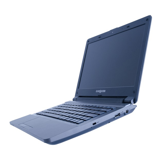
Related Manuals for EUROCOM D500P


Summary of Contents for EUROCOM D500P
- Page 3 Preface Notebook Computer D500P/D510P/D520P/D530P Service Manual...
- Page 4 Preface Notice The company reserves the right to revise this publication or to change its contents without notice. Information contained herein is for reference only and does not constitute a commitment on the part of the manufacturer or any subsequent ven- dor.
-
Page 5: About This Manual
Preface About this Manual This manual is intended for service personnel who have completed sufficient training to undertake the maintenance and inspection of personal computers. It is organized to allow you to look up basic information for servicing and/or upgrading components of the computer. The following information is included: Chapter 1, Introduction, provides general information about the location of system elements and their specifications. -
Page 6: Important Safety Instructions
Preface IMPORTANT SAFETY INSTRUCTIONS When using your telephone equipment, basic safety precautions should always be followed to reduce the risk of fire, elec- tric shock and injury to persons, including the following: 1. Do not use this product near water, for example near a bath tub, wash bowl, kitchen sink or laundry tub, in a wet basement or near a swimming pool. -
Page 7: Instructions For Care And Operation
Preface Instructions for Care and Operation The notebook computer is quite rugged, but it can be damaged. To prevent this, follow these suggestions: Don’t drop it, or expose it to shock. If the computer falls, the case and the components could be damaged. Do not expose the computer Do not place it on an unstable Do not place anything heavy... -
Page 8: Power Safety
Preface Avoid interference. Keep the computer away from high capacity transformers, electric motors, and other strong mag- netic fields. These can hinder proper performance and damage your data. Take care when using peripheral devices. Use only approved brands of Unplug the power cord before peripherals. -
Page 9: Battery Precautions
Preface Battery Precautions • Only use batteries designed for this computer. The wrong battery type may explode, leak or damage the computer. • Recharge the batteries using the notebook’s system. Incorrect recharging may make the battery explode. • Do not try to repair a battery pack. Refer any battery pack repair or replacement to your service representative or qualified service personnel. -
Page 10: Related Documents
Preface Related Documents You may also need to consult the following manual for additional information: User’s Manual on CD This describes the computer’s features and the procedures for operating the computer and its ROM-based setup program. It also describes the installation and operation of the utility programs provided with the computer. VIII... -
Page 11: Table Of Contents
Preface Contents Introduction ..........1-1 Mainboard Overview - Bottom (Key Parts) ......... 1-10 Mainboard Overview - Top (Cable Connectors) ......1-11 Overview ..................1-1 Mainboard Overview - Bottom (Cable Connectors) ..... 1-12 System Specifications ..............1-2 Disassembly ..........2-1 Processor Types ................1-2 Core Logic ..................1-2 Overview .................. - Page 12 Battery (D500P) ................A-6 LCD 15” (D530P) ................ A-38 Card Reader (D500P) ..............A-7 Battery (D530P) ................A-39 TEAC CD-ROM Drive (D500P) ............ A-8 Card Reader (D530P) ..............A-40 KME CD-RW Drive (D500P) ............A-9 TEAC CD-ROM Drive (D530P) ..........A-41 Combo Drive (D500P) ..............
- Page 13 Preface ICH5 (2 of 3) ................B-16 ICH5 (3 of 3) ................B-17 HDD/CD-ROM/FDD ..............B-18 PCI 1410 ..................B-19 PCI1394 TSB43AB21 ..............B-20 PCI RTL8100C / RTL8110S ............B-21 LPC Super I/O ................B-22 LPC H8 ..................B-23 AC'97 Codec ................B-24 FAN/MBC/Mini PCI ..............
- Page 14 Preface...
-
Page 15: Introduction
1: Introduction Overview This manual covers the information you need to service or upgrade the D500P/D510P/D520P/D530P notebook comput- er. Information about operating the computer (e.g. getting started, and the Setup utility) is in the User’s Manual. Infor- mation about drivers (e.g. VGA & audio) is also found in User’s Manual. That manual is shipped with the computer. -
Page 16: System Specifications
Introduction System Specifications Processor Types Memory • Two 200 Pin SODIMM Sockets, Supporting DDR 266/ • Intel Pentium® 4 Processor (478-pin) m-PGA package 333/ 400 MHz Modules µ 0.13) 0.13 Micron Process Technology, • Expandable up to 1024 MB (128/256/512MB DDR Mod- 512KB On-die L2 Cache &... -
Page 17: Storage
Introduction Storage PC Card • Bay One for one of the following Interchangeable devices: • One Type II PCMCIA 3.3V/5V Socket Supporting Card- 3.5" 3-mode FDD Secondary Battery Keyboard Secondary Hard Disk Drive 6-in-1 Card Reader • Win 95 Keyboard •... -
Page 18: Communication
Introduction Communication Environmental Spec • 56K Plug & Play Modem (V.90 & V.92 Compliant) • Temperature • Infrared transfer: 115.2K bps SIR/ 4M bps FIR, IrDA 1.1 ° ° Operating: C ~ 35 compliant ° ° Non-Operating: C ~ 60 •... -
Page 19: External Locator - Top Views
Introduction External Locator - Top Views Figure 1 - 1 Top Views with LCD Panel Open 1. LCD 2. LED Power & E-Mail Indicators 3. Close Cover Switch Model Differences 4. Speakers 5. Hot-Key buttons This manual refers to the two notebook mod- 6. -
Page 20: External Locator - Front & Left Side View
Introduction External Locator - Front & Left Side View Figure 1 - 2 Front View 1. LCD Latch 2. Audio “DJ” CD Player Control Panel On/Off Switch 3. Previous Track 4. Next Track 5. LCD 6. Play Pause 7. Stop 8. -
Page 21: External Locator - Right Side & Rear Views
Introduction External Locator - Right Side & Rear Views Figure 1 - 4 Right Side View 1. Device Bay One 2. Device Bay Two 3. Infrared Transceiver Figure 1 - 5 Rear View 1. Security Lock 2. Microphone-In Jack 3. Headphone-Out Jack 4. -
Page 22: External Locator - Bottom View
Introduction External Locator - Bottom View Figure 1 - 6 Bottom View 1. Vent/Fan Intakes 2. Device Bay One 3. Device Bay One Release Latch 4. Device Bay Two 5. Device Bay Two Release Screw 6. Battery 7. Battery Release Latch 1 - 8 External Locator - Bottom View... -
Page 23: Mainboard Overview - Top (Key Parts)
Introduction Mainboard Overview - Top (Key Parts) Figure 1 - 7 Mainboard Overview - Top Key Parts 1. 2 * SO-DIMM sockets 2. AC’97 Codec 3. TI 1394 Control- 4. Flash BIOS ROM 5. Audio DJ Controller 6. PCI Bus1410 Controller Mainboard Overview - Top (Key Parts) 1 - 9... -
Page 24: Mainboard Overview - Bottom (Key Parts)
Introduction Mainboard Overview - Bottom (Key Parts) Figure 1 - 8 Mainboard Overview - Bottom Key Parts 1. CPU Socket (no CPU installed) 2. VGA Chip - ATI 3. LAN Controller - RTL8110S-32 4. Super IO NS87393 5. Southbridge Intel 82801 6. -
Page 25: Mainboard Overview - Top (Cable Connectors)
Introduction Mainboard Overview - Top (Cable Connectors) Figure 1 - 9 Mainboard Overview - Top Cable Connectors 1. JINTKB1 (Key- board Connector) 2. JTP1 (TouchPad Connector) 3. JMDC1 (Modem Connector) 4. JSPK1 (Speaker Connector) 5. JLED1 (LED Connector) 6. JLCD1 (LCD Connector) 7. -
Page 26: Mainboard Overview - Bottom (Cable Connectors)
Introduction Mainboard Overview - Bottom (Cable Connectors) Figure 1 - 10 Mainboard Overview - Bottom Cable Connectors 1. JHDD1 (Hard Disk Connector) 2. JFAN1 (Fan Connector) 3. PCMCIA Connector 4. JCD1 (Bay One Device Connector) 5. JDD1 (DC/DC Board Connector) 6. -
Page 27: Disassembly
Disassembly 2: Disassembly Overview This chapter provides step-by-step instructions for disassembling parts and subsystems. When it comes to reassembly, reverse the procedures (unless otherwise indicated). We suggest you completely review any procedure before you take the computer apart. Procedures such as upgrading/replacing the RAM, CD device and hard disk are included in the User’s Manual but are repeated here for your convenience. -
Page 28: Maintenance Tools
Disassembly NOTE: All disassembly procedures assume that the system is turned OFF, and disconnected from any power supply (the battery is removed too). Maintenance Tools The following tools are recommended when working on the notebook PC: • M3 Philips-head screwdriver •... -
Page 29: Maintenance Precautions
Disassembly Maintenance Precautions The following precautions are a reminder. To avoid personal injury or damage to the computer while performing a re- moval and/or replacement job, take the following precautions: Power Safety Warning 1. Don't drop it. Perform your repairs and/or upgrades on a stable surface. If the computer falls, the case and other Before you undertake components could be damaged. -
Page 30: Disassembly Steps
Disassembly Disassembly Steps To remove the CPU: 1. Remove the battery page 2 - 7 The following table lists the disassembly steps, and on 2. Remove the CPU page 2 - 13 which page to find the related information. PLEASE PERFORM THE DISASSEMBLY STEPS IN THE To remove the Modem: ORDER INDICATED. - Page 31 Disassembly To remove the Audio “DJ” Module: 9. Remove the Audio “DJ” module page 2 - 20 10. Remove the HDD converter board page 2 - 21 1. Remove the battery page 2 - 7 11. Remove the mainboard page 2 - 22 2.
- Page 32 Disassembly To remove the TouchPad: To remove the Inverter: 1. Remove the battery page 2 - 7 1. Remove the battery page 2 - 7 2. Remove the Bay One device page 2 - 8 2. Remove the Bay One device page 2 - 8 3.
-
Page 33: Removing The Battery
Disassembly Removing the Battery Figure 2 - 1 Battery Removal 1. Turn the computer OFF and turn it over to locate the battery release latch (Figure 2 - 1a). Sequence 2. Slide the battery release latch towards the unlock symbol. 3. -
Page 34: Removing The Bay One Device
Disassembly Removing the Bay One Device Figure 2 - 2 Bay One Device 1. Turn the computer OFF. Removal 2. Place the computer on a clean, stable surface and turn it over. Sequence 3. Locate the release latch (Figure 2 - 2a) for the Bay One device. -
Page 35: Removing The Hard Disk Drive Assembly
Disassembly Removing the Hard Disk Drive Assembly Figure 2 - 3 Hard Disk 1. Turn the computer OFF and turn it over. Removal 2. Remove the device in Bay One (see “Removing the Bay One Device” on page 2 - Sequence 3. -
Page 36: Removing The Bay Two Device
Disassembly Removing the Bay Two Device Figure 2 - 4 Bay Two Device 1. Turn OFF the computer. Removal 2. Turn the computer over. Sequence 3. Remove screw (Figure 2 - 4a). 4. Apply gentle but firm pressure at point (Figure 2 - 4b), and slide the device out of the computer. -
Page 37: Removing The Keyboard
Disassembly Removing the Keyboard Figure 2 - 5 Keyboard 1. Turn OFF the computer. Removal 2. Press the two keyboard latches at the top of the keyboard as in Figure 2 - 5a (you may need to use a small screw- Sequence driver to do this). -
Page 38: Removing The System Memory
Disassembly Removing the System Memory Figure 2 - 6 Memory Removal 1. Remove the keyboard (see page 2 - 11). Sequence 2. Remove screws (Figure 2 - 6a) from the shielding plate, and lift the plate up off the computer. 3. -
Page 39: Removing The Cpu
Disassembly Removing the CPU Figure 2 - 7 Processor 1. Turn OFF the computer and turn it over. Removal 2. Remove the screws (Figure 2 - 7a) from the CPU cover, and remove the CPU cover Sequence a. Remove the three screws and the CPU cover. - Page 40 Disassembly 4. Carefully pull the heat sink upward using the label at point (Figure 2 - 9a). Figure 2 - 9 5. Remove the heat sink (Figure 2 - 9b) from the computer. Processor 6. Unlock the processor by raising lever (Figure 2 - 9c) to the fully vertical position, and carefully lift the proces- Removal...
-
Page 41: Removing The Modem
Disassembly Removing the Modem Figure 2 - 10 Modem Removal 1. Remove the keyboard (see page 2 - 11) and shielding plate (see page 2 - 12). Sequence 2. Remove screws and carefully lift the modem up off the mainboard (Figure 2 - 10). -
Page 42: Removing The Wireless Lan
Disassembly Removing the Wireless LAN Figure 2 - 11 1. Remove the keyboard (see page 2 - 11) and shielding plate (see page 2 - 12). Wireless LAN 2. Gently pull latches & in the direction of the arrows (Figure 2 - 11) and the module will pop-up. -
Page 43: Removing The Palm Rest
Disassembly Removing the Palm Rest 1. With the computer shut down and on a level surface, raise the LCD cover. Figure 2 - 12 2. Remove the palm rest by applying gentle upward pressure with your fingers close to the area around the left Alt Palm Rest key, and the right Ctrl key (Figure 2 -... -
Page 44: Removing The Bottom Case
Disassembly Removing the Bottom Case Figure 2 - 13 Bottom Case 1. Remove the battery (page 2 - 7), bay one device (page 2 - 8), hard disk assembly (page 2 - 9), bay two device (page Removal 10), keyboard (page 2 - 11) CPU (page 2 -... - Page 45 Disassembly 3. Turn the computer around and remove screws (Figure 2 - 14) from the rear of the computer. Figure 2 - 14 Bottom Case Removal Sequence (cont’d) Remove screws from the rear of the computer. 4. Disconnect the inverter cable , touchpad cable , LED cable , LCD cable...
-
Page 46: Removing The Audio "Dj" Module
Disassembly Removing the Audio "DJ" Module Figure 2 - 16 Audio "DJ" 1. Remove the battery (page 2 - 7), bay one device (page 2 - 8), hard disk assembly (page 2 - 9), bay two device (page Module Removal 10), keyboard (page 2 - 11) CPU... -
Page 47: Removing The Hdd Converter Board
Disassembly Removing the HDD Converter Board Figure 2 - 17 HDD Converter 1. Remove the battery (page 2 - 7), bay one device (page 2 - 8), hard disk assembly (page 2 - 9), bay two device (page Board Removal 10), keyboard (page 2 - 11) CPU... -
Page 48: Removing The Mainboard
Disassembly Removing the Mainboard Figure 2 - 18 Mainboard 1. Remove the battery (page 2 - 7), bay one device (page 2 - 8), hard disk assembly (page 2 - 9), bay two device (page Removal 10), keyboard (page 2 - 11) CPU (page 2 - 13), palm rest... - Page 49 Disassembly 3. Separate the system fan cable from the mainboard Figure 2 - 19 4. Lift the mainboard and DC/DC board out of the bottom case (Figure 2 - 19a). Mainboard Removal Sequence (cont’d) a. Separate the sys- tem fan cable. b.
-
Page 50: Removing The Dc/Dc Board
Disassembly Removing the DC/DC Board Figure 2 - 20 DC/DC Board 1. Remove the battery (page 2 - 7), bay one device (page 2 - 8), hard disk assembly (page 2 - 9), bay two device (page Removal 10), keyboard (page 2 - 11) CPU (page 2 -... -
Page 51: Removing The Click Board
Disassembly Removing the Click Board Figure 2 - 21 Click Board 1. Remove the battery (page 2 - 7), bay one device (page 2 - 8), hard disk assembly (page 2 - 9), bay two device (page Removal 10), keyboard (page 2 - 11) CPU (page 2 -... -
Page 52: Removing The Led Board
Disassembly Removing the LED Board Figure 2 - 23 LED Board 1. Remove the battery (page 2 - 7), bay one device (page 2 - 8), hard disk assembly (page 2 - 9), bay two device (page Removal 10), keyboard (page 2 - 11) CPU (page 2 -... -
Page 53: Removing The Inverter
Disassembly Removing the Inverter Figure 2 - 25 LCD Removal 1. Remove the battery (page 2 - 7), bay one device (page 2 - 8), hard disk assembly (page 2 - 9), bay two device (page Sequence 10), keyboard (page 2 - 11) CPU (page 2 - 13), palm rest... -
Page 54: Removing The Lcd Panel
Disassembly Removing the LCD Panel Figure 2 - 26 LCD Removal 1. Remove the battery (page 2 - 7), bay one device (page 2 - 8), hard disk assembly (page 2 - 9), bay two device (page Sequence 10), keyboard (page 2 - 11) CPU (page 2 -... -
Page 55: Part Lists
Part Lists Appendix A: Part Lists This appendix breaks down the notebook PC’s construction into a series of illustrations. The component part numbers are indicated in the tables opposite the drawings. Note: This section indicates the manufacturer’s part numbers. Your organization may use a different system, so be sure to cross-check any relevant documentation. -
Page 56: Part List Illustration Location
Part Lists Part List Illustration Location The following table indicates where to find the appropriate part list illustration. Table A - 1 Part List Illustration Part D500P D510P D520P D530P Location page A - 3 page A - 14 page A - 25... -
Page 57: Top (D500P
Part Lists Top (D500P) Figure A - 1 Top (D500P) Top (D500P) A - 3... -
Page 58: Bottom (D500P
Part Lists Bottom (D500P) Figure A - 2 Bottom (D500P) A - 4 Bottom (D500P) -
Page 59: Lcd 15" (D500P
Part Lists LCD 15” (D500P) Figure A - 3 LCD 15” (D500P) LCD 15” (D500P) A - 5... -
Page 60: Battery (D500P
Part Lists Battery (D500P) Figure A - 4 Battery (D500P) A - 6 Battery (D500P) -
Page 61: Card Reader (D500P
Part Lists Card Reader (D500P) Figure A - 5 Card Reader (D500P) Card Reader (D500P) A - 7... -
Page 62: Teac Cd-Rom Drive (D500P
Part Lists TEAC CD-ROM Drive (D500P) Figure A - 6 CD-ROM TEAC (D500P) A - 8 TEAC CD-ROM Drive (D500P) -
Page 63: Kme Cd-Rw Drive (D500P
Part Lists KME CD-RW Drive (D500P) Figure A - 7 CD-RW KME (D500P) KME CD-RW Drive (D500P) A - 9... -
Page 64: Combo Drive (D500P
Part Lists Combo Drive (D500P) Figure A - 8 Combo (D500P) A - 10 Combo Drive (D500P) -
Page 65: Dvd-Rom Drive (D500P
Part Lists DVD-ROM Drive (D500P) Figure A - 9 DVD-ROM Drive (D500P) DVD-ROM Drive (D500P) A - 11... -
Page 66: Audio Dj (D500P
Part Lists Audio DJ (D500P) Figure A - 10 Audio DJ (D500P) A - 12 Audio DJ (D500P) -
Page 67: Floppy Disk Drive (D500P
Part Lists Floppy Disk Drive (D500P) Figure A - 11 Floppy Disk Drive (D500P) Floppy Disk Drive (D500P) A - 13... -
Page 68: Top (D510P
Part Lists Top (D510P) Figure A - 12 Top (D510P) A - 14 Top (D510P) -
Page 69: Bottom (D510P
Part Lists Bottom (D510P) Figure A - 13 Bottom (D510P) Bottom (D510P) A - 15... -
Page 70: Lcd 15" (D510P
Part Lists LCD 15” (D510P) Figure A - 14 LCD 15” (D510P) A - 16 LCD 15” (D510P) -
Page 71: Battery (D510P
Part Lists Battery (D510P) Figure A - 15 Battery (D510P) Battery (D510P) A - 17... -
Page 72: Card Reader (D510P
Part Lists Card Reader (D510P) Figure A - 16 Card Reader (D510P) A - 18 Card Reader (D510P) -
Page 73: Teac Cd-Rom Drive (D510P
Part Lists TEAC CD-ROM Drive (D510P) Figure A - 17 TEAC CD-ROM Drive (D510P) TEAC CD-ROM Drive (D510P) A - 19... -
Page 74: Kme Cd-Rw Drive (D510P
Part Lists KME CD-RW Drive (D510P) Figure A - 18 KME CD-RW Drive (D510P) A - 20 KME CD-RW Drive (D510P) -
Page 75: Combo Drive (D510P
Part Lists Combo Drive (D510P) Figure A - 19 Combo Drive (D510P) Combo Drive (D510P) A - 21... -
Page 76: Dvd-Rom Drive (D510P
Part Lists DVD-ROM Drive (D510P) Figure A - 20 DVD-ROM Drive (D510P) A - 22 DVD-ROM Drive (D510P) -
Page 77: Audio Dj (D510P
Part Lists Audio DJ (D510P) Figure A - 21 Audio DJ (D510P) Audio DJ (D510P) A - 23... -
Page 78: Floppy Disk Drive (D510P
Part Lists Floppy Disk Drive (D510P) Figure A - 22 Floppy Disk Drive (D510P) A - 24 Floppy Disk Drive (D510P) -
Page 79: Top (D520P
Part Lists Top (D520P) Figure A - 23 Top (D520P) Top (D520P) A - 25... -
Page 80: Bottom (D520P
Part Lists Bottom (D520P) Figure A - 24 Bottom (D520P) A - 26 Bottom (D520P) -
Page 81: Lcd 15" (D520P
Part Lists LCD 15” (D520P) Figure A - 25 LCD 15” (D520P) LCD 15” (D520P) A - 27... -
Page 82: Battery (D520P
Part Lists Battery (D520P) Figure A - 26 Battery (D520P) A - 28 Battery (D520P) -
Page 83: Card Reader (D520P
Part Lists Card Reader (D520P) Figure A - 27 Card Reader (D520P) Card Reader (D520P) A - 29... -
Page 84: Teac Cd-Rom Drive (D520P
Part Lists TEAC CD-ROM Drive (D520P) Figure A - 28 TEAC CD_ROM Drive (D520P) A - 30 TEAC CD-ROM Drive (D520P) -
Page 85: Kme Cd-Rw Drive (D520P
Part Lists KME CD-RW Drive (D520P) Figure A - 29 KME CD-RW Drive (D520P) KME CD-RW Drive (D520P) A - 31... -
Page 86: Combo Drive (D520P
Part Lists Combo Drive (D520P) Figure A - 30 Combo Drive (D520P) A - 32 Combo Drive (D520P) -
Page 87: Dvd-Rom Drive (D520P
Part Lists DVD-ROM Drive (D520P) Figure A - 31 DVD-ROM Drive (D520P) DVD-ROM Drive (D520P) A - 33... -
Page 88: Audio Dj (D520P
Part Lists Audio DJ (D520P) Figure A - 32 Audio DJ (D520P) A - 34 Audio DJ (D520P) -
Page 89: Floppy Disk Drive (D520P
Part Lists Floppy Disk Drive (D520P) Figure A - 33 Floppy Disk Drive (D520P) Floppy Disk Drive (D520P) A - 35... -
Page 90: Top (D530P
Part Lists Top (D530P) Figure A - 34 Top (D530P) A - 36... -
Page 91: Bottom (D530P
Part Lists Bottom (D530P) Figure A - 35 Bottom (D530P) Bottom (D530P) A - 37... -
Page 92: Lcd 15" (D530P
Part Lists LCD 15” (D530P) Figure A - 36 LCD 15” (D530P) A - 38 LCD 15” (D530P) -
Page 93: Battery (D530P
Part Lists Battery (D530P) Figure A - 37 Battery (D530P) Battery (D530P) A - 39... -
Page 94: Card Reader (D530P
Part Lists Card Reader (D530P) Figure A - 38 Card Reader (D530P) A - 40 Card Reader (D530P) -
Page 95: Teac Cd-Rom Drive (D530P
Part Lists TEAC CD-ROM Drive (D530P) Figure A - 39 TEAC CD_ROM Drive (D530P) TEAC CD-ROM Drive (D530P) A - 41... -
Page 96: Kme Cd-Rw Drive (D530P
Part Lists KME CD-RW Drive (D530P) Figure A - 40 KME CD-RW Drive (D530P) A - 42 KME CD-RW Drive (D530P) -
Page 97: Combo Drive (D530P
Part Lists Combo Drive (D530P) Figure A - 41 Combo Drive (D530P) Combo Drive (D530P) A - 43... -
Page 98: Dvd-Rom Drive (D530P
Part Lists DVD-ROM Drive (D530P) Figure A - 42 DVD-ROM Drive (D530P) A - 44 DVD-ROM Drive (D530P) -
Page 99: Audio Dj (D530P
Part Lists Audio DJ (D530P) Figure A - 43 Audio DJ (D530P) Audio DJ (D530P) A - 45... -
Page 100: Floppy Disk Drive (D530P
Part Lists Floppy Disk Drive (D530P) Figure A - 44 Floppy Disk Drive (D530P) A - 46 Floppy Disk Drive (D530P) - Page 101 Schematic Diagrams Appendix B: Schematic Diagrams This appendix has circuit diagrams of the systems PCB’s. The following table indicates where to find the appropriate schematic diagram. Diagram - Page Diagram - Page Table B - 1 System Block Diagram - Page B - 2 ICH5 (3 of 3) - Page B - 17 Schematic CPU 1 of 2 - Page B - 3...
-
Page 102: Schematic Diagrams
Schematic Diagrams System Block Diagram mPGA478B Socket for CK-409 Prescott or Northwood 10.0 VRAM 2 CHANNEL AGP 8X SPRINGDALE TV OUT 2DIMMs GMCH-PE CRT PORT Sheet 1 of 29 System Block LAN /GIGA MINI Hub Link Diagram USB Port 1 8100C USB Port 2 /8110S... -
Page 103: Cpu 1
Schematic Diagrams CPU 1 of 2 HA[0..31] DBI#0 HA[0..31] DINV#0 DBI#0 DBI#1 DBI#1 DINV#1 DBI#2 DINV#2 DBI#2 DBI#3 DBI#3 DINV#3 VID0 VID0 VID0 [27] VID1 VCCP VID1 [27] VID1 VID2 VID2 VID2 [27] VID3 VID3 [27] VID3 HA10 VID4 HA10 VID4 VID4 [27]... - Page 104 Schematic Diagrams CPU 2 of 2 VCORE- VCORE- [27] VCORE+ VCORE+ [27] VCCP VCCP AE22 VCCP VCCP AE24 VCCP VCCP VCCP AE26 TZ0301 VCCP VCCP VCCP VCCP VCCP VCCP C158 22UF/6.3V C146 22UF/6.3V VCCP VCCP AF10 VCCP VCCP AF12 AA10 VCCP VCCP AF14...
-
Page 105: Clock Generator
Schematic Diagrams Clock Generator VCCCK HCB-2012K-121T30 +3VS C327 C273 C288 C318 C286 C285 C281 C264 C265 C287 0.1UF 0.1UF 0.1UF 0.1UF 0.1UF 0.1UF 0.1UF 0.1UF 10UF/6.3V 10UF/6.3V R210 VCC48 VCCCK VDD_REF PCI_F0 R570 PCLKICH VDD_PCI1 PCIF_0 PCLKICH [15] C276 PCI_F1 VDD_PCI2 PCIF_1 C272... - Page 106 Schematic Diagrams GMCH-1 place close GMCH < 0.25" +1.5VS GCBE0 GADSTBF0 [10] GCBE0 GADSTBF0 [10] GCBE0 GADSTBF0 GCBE1 GADSTBS0 [10] GCBE1 GCBE1 GADSTBS0 GADSTBS0 [10] HA[3..31] HD-[0..63] GCBE2 GAD[0..15] HA[3..31] HD-[0..63] [2] [10] GCBE2 GCBE2 GAD[0..15] [10] GCBE3 GAD0 HD-0 R418 AGP 3.0 [10]...
-
Page 107: Gmch-2 Power
Schematic Diagrams GMCH-2 Power AR32 AE11 AR29 AE10 AR27 AR25 AR23 AD33 AR20 AD30 VCCPCAP1 AR16 AD28 +1.5VS VCCPCAP2 VCCA_FSB AR13 AD10 +1.5VS VCCPCAP3 AR11 GMCHVCCP 0.82U AN32 C465 AN30 100UF/10V C466 AN28 AC35 0.1UF AN26 AC32 AN24 AN22 AN20 AB33 AN18 AB30... - Page 108 Schematic Diagrams GMCH-3 DDR +2.5V MAAA0 AJ34 AN11 DQSA0 SMAA_A0 SDQS_A0 MAAA1 AL33 AP12 SDMA0 MAAB0 AG31 AF15 DQSB0 SMAA_A1 SDM_A0 SMAA_B0 SDQS_B0 MAAA2 AK29 AP10 MDA0 MAAB1 AJ31 AG11 SDMB0 SMAA_A2 SDQ_A0 SMAA_B1 SDM_B0 MAAA3 AN31 AP11 MDA1 MAAB2 AD27 AJ10 MDB0...
-
Page 109: Dimma
Schematic Diagrams DIMMA +2.5V +1.25V +1.25V RP64 RP65 8P4RX56_0402 8P4RX56_0402 RP44 RP45 MDA49 MDA50 8P4RX56_0402 8P4RX56_0402 JDIM1 MDA48 DQSA6 MDA0 DQSA0 MDA52 MDA54 MDA1 MDA2 MDA53 SDMA6 MDA5 MDA6 MAAA0 MDA0 MDA4 SDMA0 C234 C252 MAAA1 MDA1 C239 MAAA2 MDA2 C249 MAAA3 MDA3... -
Page 110: Dimmb
Schematic Diagrams DIMMB +1.25V +2.5V +1.25V RP73 RP74 RP93 RP94 8P4RX56_0402 8P4RX56_0402 8P4RX56_0402 8P4RX56_0402 MDB0 DQSB0 JDIM2 MDB49 MDB50 MDB1 MDB2 MDB48 DQSB6 MDB5 MDB6 MDB52 MDB54 MDB4 SDMB0 MAAB0 MDB0 MDB53 SDMB6 C295 MAAB1 MDB1 C309 C292 C316 MAAB2 MDB2 MAAB3 MDB3... -
Page 111: Agp/ Power
Schematic Diagrams AGP/ POWER VGA_CORE BGA4F BGA4A GAD[0..31] +3VS DIODE SUPPLIES POWER GAD[0..31] [5] VDDC GPIO0 GAD0 TO VDDC RAIL Part 6 of 7 GPIO0 VDDC WHEN VDDC IS OFF AND +3.3V IS ON RP40 GPIO1 Part 1 of 7 GAD1 HCB1608K-121T25 GPIO1... - Page 112 Schematic Diagrams GMC-1 +2.5/2.8 BGA4B +2.5/2.8 MEMA_MD0 MEMA_MA0 DQA0 MAA0 MEMA_MD1 Part 2 of 7 MEMA_MA1 DQA1 MAA1 MEMA_MD2 MEMA_MA2 DQA2 MAA2 MEMA_MD3 MEMA_MA3 DQA3 MAA3 MEMA_MD4 MEMA_MA4 MAA4 DQA4 MEMA_MD5 MEMA_MA5 BGA6 BGA7 DQA5 MAA5 MEMA_MD6 MEMA_MA6 2/16/32 DDR DQA6 MAA6 MEMA_MD7...
- Page 113 Schematic Diagrams GMC-2 +2.5/2.8 +2.5/2.8 BGA4C MEMB_MA0 MEMB_MD0 DQB0 MAB0 MEMB_MD1 Part 3 of 7 MEMB_MA1 DQB1 MAB1 MEMB_MD2 MEMB_MA2 DQB2 MAB2 MEMB_MD3 MEMB_MA3 DQB3 MAB3 MEMB_MD4 MEMB_MA4 BGA8 DQB4 MAB4 BGA9 MEMB_MA5 MEMB_MD5 2/16/32 DDR DQB5 MAB5 MEMB_MA6 MEMB_MD6 2/16/32 DDR DQB6 MAB6...
-
Page 114: Vga Connector
Schematic Diagrams VGA Connector PANEL CONNECTOR PVDD JLCD1 C717 +3VS +3VS 0.1UF LVDS-L0N LVDS_TXL0N [10] LVDS-L0P BAV99 BAV99 BAV99 LVDS_TXL0P [10] 0(0805) LVDS-L1N LVDS_TXL1N [10] S_IOY S_IOC LVDS-L1P LVDS_TXL1P [10] C431 0.1UF LVDS-L2N SOT-23 LVDS_TXL2N [10] LVDS-L2P LVDS_TXL2P [10] C436 0.1UF LVDS-LCLKN LVDS_TXLCKN [10]... -
Page 115: Ich5 (1
Schematic Diagrams ICH5 (1 of 3) U20D HIGH:80pin LOW :40pin U20B A20GATE P66DET# [22] A20GATE P66DET# A20GATE (5VS)AGPBUSY#/GPI6 HL[0..10] K_A20M# S66DET# HL[0..10] K_A20M# S66DET# A20M# (5VS)GPI7 USBP0 SLP# Z1407 USBP0P USBP0 [16] SLP# CPU_SLP# (3V)GPI8 EXTSMI# [22] SMBALERT USBN0 FERR# 1N4148 USBP0N USBN0... -
Page 116: Ich5 (3
Schematic Diagrams ICH5 (2 of 3) U20A AD[0..31] AD[0..31] [18,19,20,24] FRAME# AD31 [18,19,20,24] FRAME# FRAME# AD31 IRDY# AD30 U20C [18,19,20,24] IRDY# IRDY# AD30 TRDY# AD29 PIDED[0..15] SIDED[0..15] [18,19,20,24] TRDY# [17] PIDED[0..15] SIDED[0..15] [17,26] TRDY# AD29 DEVSEL# AD28 PIDED15 AB17 AA23 SIDED15 [18,19,20,24] DEVSEL#... - Page 117 Schematic Diagrams ICH5 (3 of 3) +3VS C210 U20F 22UF/6.3V C915 *0.1UF C579 0.1UF 1.1A SGND4 +1.5VS C804 22UF/6.3V C931 *0.1UF C574 0.1UF R371 470K Z1601 Z1602 [14] OC#0 C773 0.1UF HCB2012K-500T40 C904 *0.1UF C571 0.1UF C413 C418 C414 C723 0.1UF R370 C932...
-
Page 118: Hdd/Cd-Rom/Fdd
Schematic Diagrams HDD/CD-ROM/FDD HDD CONNECTOR JHDD2 OZ165 PCIRST# PCIRST# CRESETN PCIRST# [10,15,18,19,21,22,24,26] HRESETN CRESETN PIDED8 PIDED7 SIDED0 CDD[0] HDD[0] CDD[0] PIDED9 PIDED6 SIDED1 CDD[1] +5VCDROM HDD[1] CDD[1] PIDED10 PIDED5 SIDED2 CDD[2] HDD[2] CDD[2] PIDED11 PIDED4 SIDED3 CDD[3] HDD[3] CDD[3] PIDED12 PIDED3 SIDED4 CDD[4]... -
Page 119: Pci 1410
Schematic Diagrams PCI 1410 VPPD0 VCCP0 VPPD1 VCCCB PCUVCC VCCD0# HCB2012K-121T30 VCCP0 VCCD1# C885 C868 C395 C876 C842 C828 C830 C877 AD[0..31] 0.1UF 0.1UF 0.1UF 0.1UF 0.1UF 0.1UF 0.1UF 10UF/16V [15,19,20,24] AD[0..31] PCI1410 JPCM1 VPPCB CAD0 C840 C843 C841 D3 - CAD0 1000PF 0.1UF 10UF/16V... -
Page 120: Pci1394 Tsb43Ab21
Schematic Diagrams PCI1394 TSB43AB21 TSB43AB21 1 PORT 1394 TSB43AB22 2 PORT 1394 +3VS Z1902 4.7K Z1903 C106 C107 +3VS Z1904 Z1901 T214 Z1906 0.1UF 0.1UF 0.1UF 0.1UF 0.1UF 10UF/16V Z1905 4.7KX4 C445 C108 C102 C472 0.1UF 0.1UF 0.1UF 0.1UF 0.1UF 0.1UF 0.1UF AD[0..31]... -
Page 121: Pci Rtl8100C / Rtl8110S
Schematic Diagrams PCI RTL8100C / RTL8110S 8100C 8110S TRANSFORMER U6 24ST0023-3 LG-2402S R476 R380,381,379,382 Z2001 XTAL1 FRC1394-201 C534,535 0.1UF 0.01UF XTAL2 C532,533 0.01UF R497 5.6K LAN_VDD33 LAN_VDD33 CRYSTAL 25MHz Z2002 TZ2001 R448,449,450,451 49.9 LAN_VDD33 *OSC 25MHz C525,526 0.01UF C635 C603 C591 EECS LAN_VDD33... -
Page 122: Lpc Super I/O
Schematic Diagrams LPC Super I/O +3VS C809 C770 C340 C794 [14,22] LPC_AD0 0.1UF SA18 0.1UF 0.1UF 0.1UF [14,22] LPC_AD1 SA17 [14,22] LPC_AD2 SA16 [14,22] LPC_AD3 LPC_AD0 LPTD0 SA15 LAD0 PD0/INDEX# LPC_AD1 LPTD1 SA14 LAD1 PD1/TRK0# LPC_AD2 LPTD2 SA13 C787 *10PF R584 LAD2 PD2/WP#... -
Page 123: Lpc H8
Schematic Diagrams LPC H8 +3VH8 VDD5 +3VH8 Trace width 40 mil C260 0.1UF +3VH8 Z2202 Z2201 +3VH8 +3VS +3VH8 C325 C289 C275 C1005 C349 10UF/10V +5VS 0.1UF 0.1UF 0.1UF HCB3216K-800T30 1100 mA 0.1UF C421 R159 C261 C358 10UF/10V 270PF R164 0.1UF 10UF/10V R186... -
Page 124: Ac'97 Codec
Schematic Diagrams AC'97 Codec +3VS ID0 ID1 EAPD R429 RB751V *10K [22] VOLUME R464 C548 0.1UF [14] ICHSPK R404 R403 AUD_VDD AUD_VDD C539 *0.01UF XTL_IN CODECCLK14 TZ2308 C549 0.1UF BEEP [22] H8_BEEP TZ2309 AUD_VDD CODEC R432 SPDIFO TZ2310 靠近 C537 0.1UF *10K [18]... -
Page 125: Fan/Mbc/Mini Pci
Schematic Diagrams FAN/MBC/Mini PCI +5VS HCB2012K-500T40 /0805 WLESS_EN R213 WLESS_ENA [22] WLESS_EN +5VS R713 4.7K Z2423 +3VS +3VS Z2421 JMINIPCI1 AD[0..31] AD[0..31] [15,18,19,20] MAIN TZ2401 TZ2421 R714 Z2422 TZ2402 TZ2422 FAN1 RB751V TZ2403 TZ2423 C851 TZ2404 TZ2424 R385 NDS352AB C845 C355 C354 C844... -
Page 126: Acin; Pwr Button
Schematic Diagrams ACIN; PWR Button SM1040D1(TO-252) C132 *10K(0805) 0.1U(0805) +12V JAC1 +12V 0.1U(0805) RSS090N03 0(1206) R704 100m(2512) +3VS VA++ Z2526 +1.8V +1.8VS 100m(2512) R705 降低 ACIN 耗電過大 DEL:R94/R95 R706 100m(2512) C935 R304 ACIN CON C878 150K PIN GND1~5 =GND 0.1U(0805) 0.1U(0805) *10K(0805) 10K(0805) -
Page 127: D/D Conn
Schematic Diagrams D/D Conn JDD1 JDD2 CON-60 CON-60 [21] INDEX# HDSEL# [21] [21] DISKCHG# DRV0# [21,24] [21] DIR# MTR0# [21] C896 [21] STEP# 1.6M_EN# [21] 0.1UF [21] WGATE# WDATA# [21] [21] RDATA# TRK0# [21] Z2601 R258 C891 C901 [21] WRPRT# PCIRST# [10,15,17,18,19,21,22,24] 10UF/25... -
Page 128: Vcore
Schematic Diagrams VCORE AUX2 AUX1 AUX3 AUX4 R305 C775 C778 C785 +5VS R306 C344 0.47U/25V(0805) IRLR7821 0.1U(0805) Z2702 Z2701 10UF/25V(1210) 22UF/25V_OS10*5 RB751V Z2717 R610 Z2719 VCCP TZ2701 C364 R619 T247 Z2757 1U(0805) VCCP R324 0.9UH DRN4 R333 C389 C386 R318 R313 R309 R322... -
Page 129: System Power 1
Schematic Diagrams System Power 1 DDON [25,29] RUN/SS2 R359 Z2850 R702 R357 Z2831 R355 Z2801 TZ2801 TZ2802 SYS5V Z2828 RSS090N03 VDD5 LTC3728UH RSS090N03 R336 R694 C401 0.01uF Z2833 Z2829 RUN/SS1 PGOOD C930 *180pF C909 1000pF R670 SDT1205P-4R7-122 8m(1206) C870 SENSE1+ C864 C390 R695... -
Page 130: System Power 2
Schematic Diagrams System Power 2 R599 SYS5V +3VS +3VS VCCVID [25,28] DDON CM2841ACIM25 C393 C781 150mA 30 mil C905 Z2905 R588 C906 R577 30 mil Z2901 R264 Z2908 0.1uF/50V 10U_1210(25V) 10U/25V_O *10K C795 R263 R262 R596 4.7K Z2955 2.2U(0805) [15,22,25,26,28] SUSB# 560K RB751V... -
Page 131: Installing Optional Module
Appendix C: Installing Optional Module Overview This chapter provides instructions for installing optional modules. We suggest you completely review any procedure before you take the computer apart. To make the assembly process easier each section may have a box in the page margin. Information contained under the figure # will give a synopsis of the sequence of procedures involved in the disassembly/assembly procedure. -
Page 132: Installing A Bluetooth Modem
Installing a Bluetooth Modem Figure C - 1 Bluetooth Installation procedure for computers with Bluetooth modem and wireless LAN module. Modem 1. Turn the computer OFF. Installation 2. Remove the keyboard (see page 2 - 11), shielding plate (see page 2 - 12) and modem (see page 2 - 15). -
Page 133: Installing The 802.11B Wireless Lan
Installing the 802.11b Wireless LAN Figure C - 2 Installation procedure for computers with Bluetooth modem and wireless LAN module. 802.11b Wireless 1. Turn the computer OFF. LAN Installation 2. Remove the keyboard (see page 2 - 11), shielding plate (see page 2 - 12). -
Page 134: Installing The 802.11G Wireless Lan
Installing the 802.11g Wireless LAN Figure C - 3 Installation procedure for computers with Bluetooth modem and wireless LAN module. 802.11g Wireless 1. Turn the computer OFF. LAN Installation 2. Remove the keyboard (see page 2 - 11), shielding plate (see page 2 - 12).
Need help?
Do you have a question about the D500P and is the answer not in the manual?
Questions and answers