
Related Manuals for Omron DEVICENET#05-2003


Summary of Contents for Omron DEVICENET#05-2003
- Page 1 Cat. No. W348-E1-05 DRT1-COM GT1 Series DeviceNet MULTIPLE I/O TERMINAL OPERATION MANUAL...
- Page 2 DRT1-COM GT1 Series DeviceNet MULTIPLE I/O TERMINAL Operation Manual Revised May 2003...
- Page 4 PowerTap is a registered trademark of the Allen-Bradley Company, Inc. OMRON, 1998 All rights reserved. No part of this publication may be reproduced, stored in a retrieval system, or transmitted, in any form, or by any means, mechanical, electronic, photocopying, recording, or otherwise, without the prior written permission of OMRON.
-
Page 6: Table Of Contents
Specifications Common to All Basic I/O Units ........ - Page 7 Input and Output Units, and Relay Output Units. Section 5 provides the specifications for Special I/O Units, including the Analog Input Unit, the Analog Output Unit, the Temperature Input Unit, and the Counter Unit. Setting procedures for a Configurator are also provided.
- Page 8 Application Precautions ........
-
Page 9: Intended Audience
!WARNING It is extremely important that a PC System and all PC Units be used for the specified purpose and under the specified conditions, especially in applica- tions that can directly or indirectly affect human life. You must consult with your OMRON representative before applying a PC System to the abovemen- tioned applications. -
Page 10: Application Precautions
Improper installation may cause faulty operation. • Be sure to tighten Backplane screws, terminal screws, and cable connec- tor screws securely. • Do not attempt to take any Units apart, to repair any Units, or to modify any Units in any way. xiii... - Page 11 Application Precautions • Do not use communications cables or I/O cables in parallel to or close to high-tension, high-rate current carrying lines. Doing so may cause faulty operation. • Be sure to install the MULTIPLE I/O TERMINAL in the proper direction.
-
Page 12: Ec Directives
EC Directives are satisfied for the overall machine or device. 4. MULTIPLE I/O TERMINAL products that meet EC Directives have config- urations with less than 30 m of I/O wiring, and less than 10 m of power sup- ply wiring. The following examples show means of reducing noise. - Page 13 EC Directives 3. Keep DeviceNet communications cables as short as possible and ground to 100 min.
- Page 14 This section provides an overview of the MULTIPLE I/O TERMINAL, including its features and functions. MULTIPLE I/O TERMINAL........
-
Page 15: Multiple I/O Terminal
Communications Unit that interfaces one or more I/O Units. The I/O Unit interface supports up to 8 I/O Units and a total of up to 1,024 I/O points. I/O Units are connected using simple snap-on connections via I/O Unit Connect- ing Cables. -
Page 16: Features
The Communications Unit and the I/O Units are separate, and the Communi- cations Unit and the I/O Units are connected by an I/O Unit interface. I/O can be expanded simply by connecting additional I/O Units to the I/O Unit inter- face. -
Page 17: Communications Units And I/O Units
• It notifies the connection status or the status information for the I/O Units to the DeviceNet Master Unit. • It provides a DIP switch to set the node number and baud rate of the MULTIPLE I/O TERMINAL as a DeviceNet Slave. -
Page 18: List Of Models
MULTIPLE I/O TERMINAL Section 1-1 1-1-5 List of Models Unit Words allocated Unit Installa- Model number Remarks points in PC memory connections power tion supply Input Output voltage Communications Unit None Status 0 words None 24 VDC DIN track DRT1-COM... - Page 19 I/O Units. These Units belong to a group called Special I/O Units. An end connector is attached to the Communications Unit, and a 40-mm I/O Unit Connecting Cable is included with each I/O Unit. A 1-m I/O Unit Connect- ing Cable (GCN1-100) is also available.
- Page 20 Plug XW2A-2501 OMRON ing to 25- pin D-sub connectors Connec- Soldered FCN361J040-AU tors made Pressure-welded FCN367J040-AU/F FUJITSU correspond- ing to high- Crimp FCN363J040-AU density connectors Note Refer to page 219, High-density Connector Cables for MULTIPLE I/O TERMI- NALs for details.
-
Page 21: Functions
Communications stop when nine or more I/O Units are connected. Power supply over- The power supply to the I/O Units and I/ load to I/O Units O refreshing for all I/O Units are stopped when the power supply to the I/O Units through the Communications Unit exceeds 0.4 A. - Page 22 Make sure that the power supply from the Communications Unit to the I/O Consumption Units is less than the total rated output current (400 mA). The I/O interface current consumption for each I/O Unit is shown in the following table.
-
Page 23: Exchanging Data
I/O Units and registers this status as the normal configu- ration (in RAM memory). At the same time, addresses 0 to 7 are allocated to the I/O Units in ascending order from the I/O Unit closest to the Communica-... -
Page 24: Allocating I/O
MULTIPLE I/O TERMINAL based on the registered configuration. When the power to the Communications Unit is turned ON, the bits allocated to the I/ O Units can be used to check the status (bits 0 to 7 of the first word) of the Communications Unit. - Page 25 16 output bits for Unit #2 CIO 66 Unused Note 1. The unused words between I/O areas that are used cannot be used as work bits. 2. The unused words (not between I/O areas that are used) can be used as work bits.
- Page 26 The Configurator can be used to set the Communications Unit node number, first word, and number of bytes to allocate (allocation size) for input block 1 and 2 and for output block 1 and 2, as shown in the following diagram. Output block 1 or 2:...
- Page 27 16 outputs 4-point 16 outputs Analog Analog Output Unit Output Unit Allocation settings for node number 05 Allocation settings for node number 05 First word: CIO 360 First word: CIO 50 Allocation size: 3 bytes (4 words) Allocation size: 12 bytes (6 words)
-
Page 28: I/O Unit Interface Status
Master Unit is 16. Calculation Example When one GT1-DA04MX Analog Output Unit and three GT1-AD08 Analog Input Units are used, the total number of input points and output points is cal- culated as follows: Total Number of Input Points: Communications Unit (Status) + Analog Input Units x 3... - Page 29 Section 1-2 • Error I/O Unit addresses As shown in the following diagram, the status consists of two words. The first two words of the Communications Unit allocation input area in the CPU Unit are allocated for this status. Include a program section in the CPU Unit to check this status and perform error processing.
-
Page 30: I/O Configuration Changes
CPU Unit. Also change the Slave node number so that the allocation area does not overlap with any other, and re-register the scan list (first set the Scan List Enable software switch to OFF, and then set it to ON after checking the I/O size). - Page 31 Configurator. Allocation Areas Not Overlap with Other Slaves In this case, I/O area duplication will also occur on the DeviceNet, as follows: • Master Unit 7-segment display will show d0, I/O area duplication. • Master status bits 14 and 4 will turn ON.
-
Page 32: Hardware Setup And Operational Check
Specific Example ........ -
Page 33: Basic Procedure
TS indicators for I/O Units: Lit green Check that the data for the I/O words allocated in the I/O memory (with default allocations, in the DeviceNet area) of the CPU Unit of the PC is being correctly read and written by the CPU Unit. -
Page 34: Specific Example
Each Communications Unit for the MULTIPLE I/O TERMINAL can be con- nected to a combined total of 1,024 input and output points (64 words) max. (This figure does not include the 2 words of the input area allocated to the I/O Unit interface status.) In this example, the following configuration will be used: •... - Page 35 Communications Unit.) To connect each pair of Units, connect I/O Unit interface communications connector 2 on the Unit closer to the Communications Unit to I/O Unit in- terface communications connector 1 on the Unit closer to the end Unit. Note The connecting cable for the I/O Unit is shown below.
- Page 36 For details of the I/O Unit interface current consumption for the Units, refer to page 9, I/O Interface Current Consumption. Select power supplies for the I/O Units that are suitable for the load currents to be used and the Units’ internal drive currents (refer to page 41).
- Page 37 • I/O Unit interface error output (low-clear output/high-clear output) for Analog Output Units. Note a) When using a DIP switch, the input and output ranges for the An- alog Input and Output Units can be set in 2-point units, whereas with a Configurator, a setting can be made for each point.
- Page 38 IR 63 For another node IR 363 • The first two words of the input area is automatically allocated for the I/O Unit interface status information. This allocation cannot be changed. • Words are allocated for the input/output data for each I/O Unit in the order that the I/O Units are connected (I/O Unit interface addresses 0 to 3) in the input area (input) and the output area (output).
-
Page 39: Sample Programs
This section provides some examples of programs used with the Counter Unit. Examples of Counter Unit Operation ....... -
Page 40: Examples Of Counter Unit Operation
Setting and control for the Counter Unit is executed by writing to the allocated area in the output area of the Master, and status check and monitoring is exe- cuted by reading the allocated area in the input area of the Master. The allo- cated area for the Counter Unit, with the system configuration shown above, is given below (this example is for fixed allocation). - Page 41 (O: positive, F: negative) Bit 00: Set value 1 (0: Not set, 1: Set) Bit 01: Set value 2 is set (0: Not set, 1: Set) Bit 02: Count value is set (0: Not set, 1: Set) Bit 03: Data code change (0: BCD, 1: Hex.)
- Page 42 (O: positive, F: negative) -: Undefined Bit 00: Set value 1 setting completion (0: Not complete, 1: Completed) Bit 01: Set value 2 setting completion (0: Not complete, 1: Completed) Bit 02: Count value setting completion (0: Not complete, 1: Completed) Bit 03: Data code status (0: BCD, 1: Hex.)
-
Page 43: Present Count Value Reading
0. 2. Setting and reading will not be executed if a bit with a higher priority is ON. As shown in the following example, therefore, it is recommended that word n+2 be used with the MOV instruction. - Page 44 Bit 23200 is a Step Advance Flag. 23200 35500 23202 MOV(21) When the Step Advance Flag 23200 turns ON and Set 1 Setting set value 1 has been set, set value 2 will be set under #0000 Completion the following conditions: Flag Words 51, 52 23201...
-
Page 45: Count Restart Operation After Error Clearance
3-1-4 Count Restart Operation after Error Clearance If power supply from the I/O Unit interface to the Counter Unit is interrupted, the Counter Unit will stop count operation. It will be necessary to restart the count operation. When the Counter Unit is restarted, all settings, such as the setting values, the present value, and the count mode will be cleared. -
Page 46: Basic I/O Unit Specifications
Communications Unit........ -
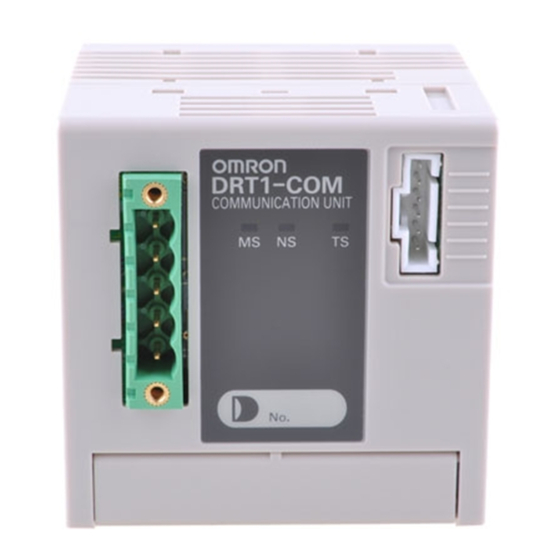
Page 47: Communications Unit
Approx. 135 g Safety standards UL508, CSA22.2 EMC directives EN50081-2, EN50082-2 This product has been tested in the test laboratory of a third party authorized by ODVA and has been approved as conforming to ODVA Conformance Soft- ware Ver. 2.0-1.00. - Page 48 All output data will be retained when a communications error occurs. (See note Note 1. I/O Units with individual settings, such as Analog Output Units, do not fol- low this setting; they follow their own setting. 2. Always turn OFF the power supplies (including the communications power...
- Page 49 Node numbers vary according to the settings of pins 1 to 6, as shown in the following table. Node numbers can be set to any value within the range, as long as they do not coincide with other nodes (Master, Slave) or node num- bers in the same network.
- Page 50 6.0 mm max. Power supply 24 VDC Dimensions Note The vertical center of the Unit is 4.9 mm lower than the center of the DIN track. The Unit therefore extends downward 41.4 mm (including the mounting hook) from the DIN track center.
-
Page 51: Specifications Common To All Basic I/O Units
Specifications Common to All Basic I/O Units Section 4-2 Specifications Common to All Basic I/O Units For details of the differences between Units, refer to the explanations for the relevant Units. General Specifications Item Specification I/O power Voltage range +10% 20.4 to 26.4 VDC (24 VDC... - Page 52 Specifications Common to All Basic I/O Units Section 4-2 Current Consumption and Weight The following table shows the current consumption, the weight and the con- nector-lock strength for the I/O Units. Model I/O Unit interface power I/O power supply current...
-
Page 53: Precautions For Connecting A Dc 2-Wire Sensor
Transistor Input Unit ON Voltage and Sensor Residual Voltage – V I/O supply voltage (Supply voltage range is 20.4 to 26.4 V, but is calculated at 20.4 V as the worst-case scenario.) ON voltage for the Transistor Input Unit (15 V with a MULTIPLE I/O TERMINAL) -
Page 54: Ts Indicator
Specifications Common to All Basic I/O Units Section 4-2 4-2-2 TS Indicator The TS indicator is a 2-color LED. The color of the TS indicator, and whether it is lit or not, indicate the following: Indicator Color State Meaning Green... -
Page 55: Transistor Input Units
Transistor Input Units Section 4-3 Transistor Input Units 4-3-1 GT1-ID16 Transistor Input Unit with Terminal Block (NPN) Input Specifications Item Specifications Number of input points 16 points Number of points that can be ON simultaneously 16 points max. Components (Refer to page 200.) - Page 56 1 A. Dimensions Approx. 89 (Unit: mm) Note The vertical center of the Unit is 4.9 mm lower than the center of the DIN track. The Unit therefore extends downward 41.4 mm (including the mounting hook) from the DIN track center.
-
Page 57: Gt1-Id16-1 Transistor Input Unit With Terminal Block (Pnp)
Transistor Input Units Section 4-3 4-3-2 GT1-ID16-1 Transistor Input Unit with Terminal Block (PNP) Input Specifications Item Specifications Number of input points 16 points Number of points that can be ON simultaneously 16 points max. Components (Refer to page 200.) - Page 58 1 A. Dimensions Approx. 89 (Unit: mm) Note The vertical center of the Unit is 4.9 mm lower than the center of the DIN track. The Unit therefore extends downward 41.4 mm (including the mounting hook) from the DIN track center.
-
Page 59: Gt1-Id16Mx Transistor Input Unit With Connector (Npn)
GT1-ID16MX Transistor Input Unit with Connector (NPN) Input Specifications Item Specifications Number of input points 16 points Number of points that can be ON simultaneously 16 points max. Components TS Indicator (Refer to page 200.) Input Indicators I/O Unit Interface Display the status of the inputs. - Page 60 Wire colors in parentheses are the previous JIS colors for photoelectric and proximity sensors. Note V terminals and V connector pins, as well as G terminals and G connector pins, are internally connected. When the I/O power is being supplied from a terminal block, the power can be supplied to the input devices from the V and G connectors.
-
Page 61: Gt1-Id16Mx-1 Transistor Input Unit With Connector (Pnp)
Dimensions Approx. 70 (Unit: mm) Note The vertical center of the Unit is 4.9 mm lower than the center of the DIN track. The Unit therefore extends downward 41.4 mm (including the mounting hook) from the DIN track center. 4-3-4... - Page 62 Terminal Arrangement Input Input Connector Pin The arrangement of the connectors is shown in the following diagram. Arrangement Wiring Attach MOLEX connectors to the Transistor Input Unit and connect them to external devices. Applicable Connectors Manufact Connector Model number Remarks...
-
Page 63: Gt1-Id16Ml Transistor Input Unit With Connector (Npn)
Dimensions Approx. 70 (Unit: mm) Note The vertical center of the Unit is 4.9 mm lower than the center of the DIN track. The Unit therefore extends downward 41.4 mm (including the mounting hook) from the DIN track center. 4-3-5... - Page 64 Communications Connector 2 (on the terminator side) Digital Input Connector (made by FUJITSU) Connects to input devices, such as switches and sensors, via an I/O Block or a Connector-Terminal Block Conversion Unit. Terminal Block DIN Track Mounting Hook Internal Circuits...
- Page 65 Function Pin number Function Wiring Attach a FUJITSU connector to the Transistor Input Unit and connect it to the external devices. Applicable Connectors Three types of connectors can be attached to the cable depending on the assembly method. When creating your own cables, use one of the following connectors.
-
Page 66: Gt1-Id16Ml-1 Transistor Input Unit With Connector (Pnp)
Dimensions (Unit: mm) Approx. 59 Note The vertical center of the Unit is 4.9 mm lower than the center of the DIN track. The Unit therefore extends downward 41.4 mm (including the mounting hook) from the DIN track center. 4-3-6... - Page 67 NC NC Function Wiring Attach a FUJITSU connector to the Transistor Input Unit and connect it to the external devices. Applicable Connectors Three types of connectors can be attached to the cable depending on the assembly method. When creating your own cables, use one of the following connectors.
-
Page 68: Gt1-Id16Ds Transistor Input Unit With Connector (Npn)
Dimensions (Unit: mm) Approx. 59 Note The vertical center of the Unit is 4.9 mm lower than the center of the DIN track. The Unit therefore extends downward 41.4 mm (including the mounting hook) from the DIN track center. 4-3-7... - Page 69 I/O Unit Interface Communications Connector 2 (on the terminator side) 25-pin D-sub Connector (female) Connects to input devices, such as switches and sensors, via an I/O Block or a Connector-Terminal Block Conversion Unit. Terminal Block DIN Track Mounting Hook Internal Circuits...
- Page 70 Plug Dimensions (Unit: mm) Approx. 59 Note The vertical center of the Unit is 4.9 mm lower than the center of the DIN track. The Unit therefore extends downward 41.4 mm (including the mounting hook) from the DIN track center.
-
Page 71: Gt1-Id16Ds-1 Transistor Input Unit With Connector (Pnp)
16 points Number of points that can be ON simultaneously 16 points max. Note The number of input points that can be ON simultaneously depends on the ambient temperature, as shown below. Max. No. of input points Ambient temperature ( C) - Page 72 Plug Dimensions (Unit: mm) Approx. 59 Note The vertical center of the Unit is 4.9 mm lower than the center of the DIN track. The Unit therefore extends downward 41.4 mm (including the mounting hook) from the DIN track center.
-
Page 73: Gt1-Id32Ml Transistor Input Unit With High-Density Connector (Npn)
GT1-ID32ML Transistor Input Unit with High-density Connector (NPN) Input Specifications Item Specifications Number of input points 32 points Number of points that can be ON simultaneously 32 points max. Components (Refer to page 200.) TS Indicator Input Indicators I/O Unit Interface Display the status of the inputs. - Page 74 XW2B-40G5 G79-I@C-@ I/O Block G7TC-I@16 Note Make sure there are no more than 16 points are turned ON at the same time. Dimensions Approx. 70 (Unit: mm) Note The vertical center of the Unit is 4.9 mm lower than the center of the DIN track.
-
Page 75: Gt1-Id32Ml-1 Transistor Input Unit With High-Density Connector (Pnp)
Transistor Input Units Section 4-3 4-3-10 GT1-ID32ML-1 Transistor Input Unit with High-density Connector (PNP) Input Specifications Item Specifications Number of input points 32 points Number of points that can be ON simultaneously 32 points max. Components TS Indicator (Refer to page 200.) - Page 76 Connector-Terminal Block Conversion Unit XW2B-40G4 or XW2B-40G5 Note Make sure there are no more than 16 points are turned ON at the same time. Dimensions Approx. 70 (Unit: mm) Note The vertical center of the Unit is 4.9 mm lower than the center of the DIN track.
-
Page 77: Transistor Output Units
Transistor Output Units Section 4-4 Transistor Output Units 4-4-1 GT1-OD16 Transistor Output Unit with Terminal Block (NPN) Output Specifications Item Specifications Number of outputs 16 points Current per common 4 A max. Components (Refer to page 200.) TS Indicator Output Indicators I/O Unit Interface Display the status of the outputs. - Page 78 Note V terminals and G terminals are internally connected. When the I/O power is being supplied, the power can be supplied to the output devices from the V terminals and G terminals. Current supplied in this way, however, must be less...
-
Page 79: Gt1-Od16-1 Transistor Output Unit With Terminal Block (Pnp)
Dimensions Approx. 89 (Unit: mm) Note The vertical center of the Unit is 4.9 mm lower than the center of the DIN track. The Unit therefore extends downward 41.4 mm (including the mounting hook) from the DIN track center. 4-4-2... - Page 80 Transistor Output Units Section 4-4 Internal Circuits Low voltage Drive power supply Output 0 Photo- coupler Drive power supply Output 1 Photo- Drive coupler power supply Terminal Arrangement Row A Row B Row C Terminal numbers...
- Page 81 4 A. Dimensions Approx. 89 (Unit: mm) Note The vertical center of the Unit is 4.9 mm lower than the center of the DIN track. The Unit therefore extends downward 41.4 mm (including the mounting hook) from the DIN track center.
-
Page 82: Gt1-Od16Mx Transistor Output Unit With Connector (Npn)
Transistor Output Units Section 4-4 4-4-3 GT1-OD16MX Transistor Output Unit with Connector (NPN) Output Specifications Item Specifications Number of outputs 16 points Current per common 2 A max. Components TS Indicator (Refer to page 200.) Output Indicators I/O Unit Interface Display the status of the outputs. - Page 83 Solenoids, valves, etc. Note V terminals and V connector pins, as well as G terminals and G connector pins, are internally connected. When the I/O power is being supplied from a terminal block, the power can be supplied to the output devices from the V and G connectors.
-
Page 84: Gt1-Od16Mx-1 Transistor Output Unit With Connector (Pnp)
Dimensions Approx. 70 (Unit: mm) Note The vertical center of the Unit is 4.9 mm lower than the center of the DIN track. The Unit therefore extends downward 41.4 mm (including the mounting hook) from the DIN track center. 4-4-4... - Page 85 Terminal Arrangement Output Output Connector Pin Arrangement The following diagram shows the pin arrangement for the connector. Wiring Attach MOLEX connectors to the Transistor Output Unit and connect them to external devices. Applicable Connectors Manufac- Connector Model number Remarks...
- Page 86 2 A. Dimensions Approx. 70 (Unit: mm) Note The vertical center of the Unit is 4.9 mm lower than the center of the DIN track. The Unit therefore extends downward 41.4 mm (including the mounting hook) from the DIN track center.
-
Page 87: Gt1-Od16Ml Transistor Output Unit With Connector (Npn)
Communications Connector 2 (on the terminator side) Digital Output Connector (made by FUJITSU) Connects to the output devices, such as relays and solenoids, via an I/O Block or a Connector-Terminal Block Conversion Unit. Terminal Block DIN Track Mounting Hook Internal Circuits... - Page 88 G connectors. Current supplied in this way, however, must be less than 2 A. If, instead of using the V and G connectors, the power supply is wired to the terminal block as shown in the following diagram, the current supplied must be less than 2.5 A.
-
Page 89: Gt1-Od16Ml-1 Transistor Output Unit With Connector (Pnp)
Dimensions (Unit: mm) Approx. 59 Note The vertical center of the Unit is 4.9 mm lower than the center of the DIN track. The Unit therefore extends downward 41.4 mm (including the mounting hook) from the DIN track center. 4-4-6... - Page 90 OUT OUT OUT OUT OUT OUT OUT Function Wiring Attach a FUJITSU connector to the Transistor Output Unit and connect it to external devices. Applicable Connectors Three types of connectors can be attached to the cable, depending on the assembly method. When creating your own cables, use one of the following connectors.
- Page 91 G connectors. Current supplied in this way, however, must be less than 2 A. If, instead of using the V and G connectors, the power supply is wired to the terminal block as shown in the following diagram, the current supplied must be less than 2.5 A.
-
Page 92: Gt1-Od16Ds Transistor Output Unit With Connector (Npn)
Communications Connector 2 (on the terminator side) 25-pin D-sub Connector (female) Connects to the output devices, such as relays and solenoids, via an I/O Block or a Connector-Terminal Block Conversion Unit. Terminal Block DIN Track Mounting Hook Internal Circuits Low voltage... - Page 93 2.5 A. Dimensions (Unit: mm) Approx. 59 Note The vertical center of the Unit is 4.9 mm lower than the center of the DIN track. The Unit therefore extends downward 41.4 mm (including the mounting hook) from the DIN track center.
-
Page 94: Gt1-Od16Ds-1 Transistor Output Unit With Connector (Pnp)
Communications Connector 2 (on the terminator side) 25-pin D-sub Connector (female) Connects to the output devices, such as relays and solenoids, via an I/O Block or a Connector-Terminal Block Conversion Unit. Terminal Block DIN Track Mounting Hook Internal Circuits Low voltage... - Page 95 2.5 A. Dimensions (Unit: mm) Approx. 59 Note The vertical center of the Unit is 4.9 mm lower than the center of the DIN track. The Unit therefore extends downward 41.4 mm (including the mounting hook) from the DIN track center.
-
Page 96: Gt1-Od32Ml Transistor Output Unit With High-Density Connector (Npn)
Communications Connector 2 (on the terminator side) High-density Digital Output Connector (made by FUJITSU) Connects to the output devices, such as relays and solenoids, via an I/O Block or a Connector-Terminal Block Conversion Unit. DIN Track Mounting Hook Terminal Block... - Page 97 G connectors. Current supplied in this way, however, must be less than 2 A. If, instead of using the V and G connectors, the power supply is wired to the terminal block as shown in the following diagram, the current supplied must be less than 4 A.
- Page 98 Dimensions Approx. 70 (Unit: mm) Note The vertical center of the Unit is 4.9 mm lower than the center of the DIN track. The Unit therefore extends downward 41.4 mm (including the mounting hook) from the DIN track center. 4-4-10 GT1-OD32ML-1 Transistor Output Unit with High-density...
- Page 99 OUT OUT OUT Function m+1 word Wiring Attach a FUJITSU connector to the Transistor Output Unit and connect it to external devices. Applicable Connectors Three types of connectors can be attached to the cable, depending on the assembly method. When creating your own cables, use one of the following connectors.
- Page 100 G connectors. Current supplied in this way, however, must be less than 2 A. If, instead of using the V and G connectors, the power supply is wired to the terminal block as shown in the following diagram, the current supplied must be less than 4 A.
-
Page 101: Relay Output Units
100 mA at 5 VDC (P level reference value) Insulation resistance 1,000 M Reference Data For details about the Relay characteristics, refer to G2R-1-SN in the PCB Relays Catalog (X033). The following table shows the life expectancy for the G2R-1-SN Relay. Item... - Page 102 Relay Output Units Section 4-5 Internal Circuits 24 VDC I/O power supply Photo- coupler Photo- coupler Terminal Arrangement Wiring 24 VDC AC (DC power supply is also possible) I/O power Independent commons supply are also possible.
-
Page 103: Gt1-Ros16 Relay Output Unit With Miniature Relay
Approx. 82 Approx. 68 (Unit: mm) Note The vertical center of the Unit is 4.9 mm lower than the center of the DIN track. The Unit therefore extends downward 41.4 mm (including the mounting hook) from the DIN track center. - Page 104 I/O Unit Interface Communications Connector 2 (on the terminator side) Terminal Block (Refer to page 200.) TS Indicator DIN Track Mounting Hook Note For details on how to replace Relays, refer to page 206. Internal Circuits Photo- coupler Photo- coupler...
- Page 105 I/O power supply Mounting Be sure to mount the Unit in one of the directions shown in the following dia- gram. If the Unit is not mounted correctly, there is a risk that the service life will be reduced. DIN Track...
- Page 106 Section 4-5 Dimensions Approx. 82 (Unit: mm) Note The vertical center of the Unit is 4.9 mm lower than the center of the DIN track. The Unit therefore extends downward 41.4 mm (including the mounting hook) from the DIN track center.
-
Page 107: Special I/O Unit Specifications
GT1-AD08MX......... -
Page 108: Analog Input Units
Averaging function Settable (via DIP switch) Open circuit detection Provided (with a range of 1 to 5 V or 4 to 20 mA) Dielectric strength 500 VAC; detected current 1 mA (between communications section and analog input, and between internal power sup-... - Page 109 DIN Track Mounting Hook DIP Switch Settings The DIP switch is on the left side of the Cassette of the Analog Input Unit (GT1-AD04). Detach the Cassette from the Unit in order to make DIP switch settings. The following diagram shows the functions of the DIP switch.
- Page 110 Analog Input Units Section 5-1 Input Range Settings As shown in the following table, the DIP switch input range settings are for two inputs each. Pin 1 Pin 2 Pin 3 Input range for inputs 0 and 1 Pin 4...
- Page 111 The –10- to 10-V range corresponds to the hexadecimal values F448 to 0BB8 (–3000 to 3000). The entire data range is F31C to 0CE4 (–3300 to 3300). A negative voltage is expressed as a two’s complement (16 bits). If the line is disconnected, the data will be the same as an input of 0 V (0000 Hex).
- Page 112 The 1- to 5-V range corresponds to the hexadecimal values 0000 to 1770 (0 to 6000). The entire data range is FED4 to 189C (–300 to 6300). If the input voltage falls below 0.8 V, the open-circuit detection function will activate and the converted data will be set to 7FFF.
- Page 113 The open-circuit detection function is activated when the input range is set to Function 1 to 5 V and the voltage drops below 0.8 V, or when the input range is set to 4 to 20 mA and the current drops below 3.2 mA. When the open-circuit detec- tion function is activated, the converted data will be set to 7FFF.
- Page 114 This voltage will be approximately 1/3 to 1/2 of the output of the input devices in the part of the circuit that is not open. (The same will apply if an open circuit occurred at B.) With such a voltage present in the circuit, the open-circuit will not be detected.
- Page 115 Section 5-1 Dimensions Approx. 80 (Unit: mm) Note The vertical center of the Unit is 4.9 mm lower than the center of the DIN track. The Unit therefore extends downward 41.4 mm (including the mounting hook) from the DIN track center.
-
Page 116: Gt1-Ad08Mx
Averaging function Settable (via DIP switch) Open circuit detection Provided. (with a range of 1 to 5 V or 4 to 20 mA) Dielectric strength 500 VAC; detected current 1 mA (between communications section and analog input, and between internal power sup-... - Page 117 The following diagram shows the functions of the DIP switch. Input range Operation specifications Averaging Switching between 4 and 8 inputs. Software setting enable/disable The following table summarizes the DIP switch settings. (All pins are factory- set to OFF.) Pin(s) Function Settings Meaning...
- Page 118 Section 5-1 Note When setting the input range using a DeviceNet Configurator, use version 1.11 or later. (If pin 16 is ON, and a setting is made using the Configurator, the input ranges will all be 0 to 5 V.) Make sure the I/O Unit power supply (including the I/O Unit interface power supply) is OFF when setting the DIP switch.
- Page 119 The –10- to 10-V range corresponds to the hexadecimal values F448 to 0BB8 (–3000 to 3000). The entire data range is F31C to 0CE4 (–3300 to 3300). A negative voltage is expressed as a two’s complement (16 bits). If the line is disconnected, the data will be the same as an input of 0 V (0000 Hex).
- Page 120 The 1- to 5-V range corresponds to the hexadecimal values 0000 to 1770 (0 to 6000). The entire data range is FED4 to 189C (–300 to 6300). If the input voltage falls below 0.8 V, the open-circuit detection function will activate and the converted data will be set to 7FFF.
- Page 121 ON will be output after averaging eight samples. Open-circuit Detection The open-circuit detection function is activated when the input range is set to Function 1 to 5 V and the voltage drops below 0.8 V, or when the input range is set to 4...
- Page 122 This voltage will be approximately 1/3 to 1/2 of the output of the input devices in the part of the circuit that is not open. (The same will apply if an open circuit occurred at B.) With such a voltage present in the circuit, the open-circuit will not be detected.
- Page 123 4 ms for all 4 points. Dimensions Approx. 70 (Unit: mm) Note The vertical center of the Unit is 4.9 mm lower than the center of the DIN track. The Unit therefore extends downward 41.4 mm (including the mounting hook) from the DIN track center.
-
Page 124: Settings Using The Configurator
The input range for the Analog Input Unit can be set using version 1.11 or later of the DeviceNet Configurator (referred to as the Configurator below). Using Ver. 1.20 or later, you can also adjust or clear the offset and gain set- tings. - Page 125 Analog Input Units Section 5-1 5. Click Set on the right of the Analog Input Unit to be set. Unit 1 to Unit 8 correspond to I/O Units #0 to #7. The Edit Unit Parameters window for the Analog Input Unit will be dis- played.
- Page 126 Analog Input Units Section 5-1 The input range will be set and the window for step 6 will appear again. 8. To change other input ranges, repeat steps 6 and 7. 9. When all the required input ranges have been changed, click OK in the Edit Unit Parameters window of the Analog Input Unit.
- Page 127 Configurator Ver. 1.20 or later. Check the label on the front on the Unit for whether the offset and gain can be adjust- ed. Offset and gain can be adjusted only if the letter B appears on the label as shown below.
- Page 128 Analog Input Units Section 5-1 actual value due to the features of the Unit or the method of connection being used. E.g.: Input range is 0 to 10 V Conversion data Hexadecimal (Decimal) After adjustment Before adjustment Voltage 10 V The possible range of gain adjustment depends on the input range.
- Page 129 The Edit Device Parameters Window for the selected Communications Unit will be displayed. 5. Click Set on the right of the Analog Input Unit to be set. Unit 1 to Unit 8 correspond to I/O Units #0 to #7. The Edit Unit Parameters Window for the Analog Input Unit will be dis-...
- Page 130 The offset will be set so that the input voltage or input current are converted to a value of 0%, and the value of the offset will be stored in the EEPROM in the Analog Input Unit. Reset the Unit to enable the new setting.
- Page 131 The gain will be adjusted so that the input voltage or input current will be converted to a value of 100%, and the value of the gain will be stored in the EEPROM in the Analog Input Unit. Reset the Unit to enable the new set- ting.
- Page 132 Analog Input Units Section 5-1 4. Click Set on the right of the Analog Input Unit to be set. Unit 1 to Unit 8 correspond to I/O Units #0 to #7. The Edit Unit Parameters Window for the Analog Input Unit will be dis- played.
- Page 133 7. A message asking you to confirm will appear. Click Yes. The offset and gain settings stored in the EEPROM in the Analog Input Unit will be reset to the default values. Reset the Unit to enable the default settings.
-
Page 134: Analog Output Units
Characteristics Item Specification Voltage outputs Current outputs Output signal range 0 to 5 V, 1 to 5 V, 0 to 10 V, or 4 to 20 mA –10 to 10 V Allowable external out- 5 K min. min. put load resistance External output imped- max. - Page 135 The following diagram shows the functions of the DIP switch. Output Operating specifications range Output for communications errors Software setting enable/disable The following table summarizes the DIP switch settings. (All pins are factory- set to OFF.) Pin(s) Function Settings Meaning...
- Page 136 DeviceNet Configurator, use version 1.11 or later. (If pin 10 is ON, and a setting is made using the Configurator, the output ranges will all be 0 to 5 V and the output for communications errors setting will be set to clear to min- imum.)
- Page 137 1 to 5 V The hexadecimal values 0000 to 1770 (0 to 6000) correspond to an analog voltage range of 1 to 5 V. The entire output range is 0.8 to 5.2 V. Voltage 5.2 V 0.8 V...
- Page 138 The hexadecimal values F448 to 0BB8 (–3000 to 3000) correspond to an ana- log voltage range of –10 to 10 V. The entire output range is –11 to 11 V. Spec- ify a negative voltage as a two’s complement (16 bits).
- Page 139 Analog Output Units Section 5-2 4 to 20 mA The hexadecimal values 0000 to 1770 (0 to 6000) correspond to an analog current range of 4 to 20 mA. The entire output range is 3.2 to 20.8 mA. Current 20.8 20 mA 4 mA 3.2 mA...
-
Page 140: Gt1-Da04Mx
Dimensions Approx. 80 (Unit: mm) Note The vertical center of the Unit is 4.9 mm lower than the center of the DIN track. The Unit therefore extends downward 41.4 mm (including the mounting hook) from the DIN track center. 5-2-2... - Page 141 Section 5-2 Characteristics Item Specification Output signal range 0 to 5 V, 1 to 5 V, 0 to 10 V, or –10 to 10 V (Current output not possible) Allowable external out- 5 K min. put load resistance External output imped- max.
- Page 142 1. When setting the output range or output for communications errors using a DeviceNet Configurator, use version 1.11 or later. (If pin 10 is ON, and a setting is made using the Configurator, the output ranges will all be 0 to 5 V and the output for communications errors setting will be set to clear to minimum.)
- Page 143 Section 5-2 output for communications errors When clear to minimum, clear to maximum, or clear to 0 V is set using DIP switch pins 8 and 9, a communications error will be output according to the output range, as shown in the following table.
- Page 144 1 to 5 V The hexadecimal values 0000 to 1770 (0 to 6000) correspond to an analog voltage range of 1 to 5 V. The entire output range is 0.8 to 5.2 V. Voltage 5.2 V 0.8 V...
- Page 145 The hexadecimal values F448 to 0BB8 (–3000 to 3000) correspond to an ana- log voltage range of –10 to 10 V. The entire output range is –11 to 11 V. Spec- ify a negative voltage as a two’s complement (16 bits).
- Page 146 Analog Output Units Section 5-2 Output Status after Pins 8 and 9 of the DIP switch determine the status of the outputs after a com- Communications Error munications error occurs in DeviceNet or I/O Unit interface communications. Settings Output status after communications error...
-
Page 147: Settings Using The Configurator
Ranges can be set in 2-point units using DIP switches. 1,2,3... 1. Set pin 10 of the DIP switch for the Analog Output Unit to ON to set the Software Setting Enable/Disable setting to enable. 2. Turn the power supply ON for all the Units of the MULTIPLE I/O TERMI- NAL, including the Analog Unit and the Communications Unit. - Page 148 Analog Output Units Section 5-2 5. Click Set on the right of the Analog Output Unit to be set. Unit 1 to Unit 8 correspond to I/O Units #0 to #7. The Edit Unit Parameters window for the Analog Output Unit will be dis- played.
- Page 149 Output Range output for communications errors (Error Output) The output range will be set and the window for step 6 will appear again. 8. To change other output ranges, repeat steps 6 and 7. 9. When all the required output ranges have been changed, click OK in the Edit Unit Parameters window of the Analog Output Unit.
- Page 150 Configurator Ver. 1.20 or later. Check the label on the front on the Unit for whether the offset and gain can be ad- justed. Offset and gain can be adjusted only if the letter B appears on the label as shown below.
- Page 151 100%. Gain adjustment is used when the greater the output voltage and output current, the greater the differ- ence from the actual value due to the features of the Unit or the method of connection being used.
- Page 152 Unit to which the Analog Output Unit is connected. The Edit Device Parameters Window for the selected Communications Unit will be displayed. 5. Click Set on the right of the Analog Output Unit to be set. Unit 1 to Unit 8 correspond to I/O Units #0 to #7.
- Page 153 6. Click Adjustment. The Unit Adjustment Window will be displayed. 7. Click the Down Arrow and select the output words and the output range to be adjusted. 8. Drag the Offset Output Slide Bar to adjust the value, and then click Set.
- Page 154 9. Click Fix Offset Value when the voltage output or current output is correct for 0%. The offset value set using the slider bar will be stored in the EEPROM in the Analog Output Unit. Reset the Unit to enable the new setting.
- Page 155 11. Click Fix Gain Value when the voltage output or current output is correct for 100%. The gain value set using the slider bar will be stored in the EEPROM in the Analog Output Unit. Reset the Unit to enable the new setting.
- Page 156 The Edit Device Parameters Window for the selected Communications Unit will be displayed. 4. Click Set on the right of the Analog Output Unit to be cleared. Unit 1 to Unit 8 correspond to I/O Units #0 to #7. The Edit Unit Parameters Window for the Analog Output Unit will be dis-...
- Page 157 7. A message asking you to confirm will appear. Click Yes. The offset and gain settings stored in the EEPROM in the Analog Output Unit will be reset to the default values. Reset the Unit to enable the default settings.
-
Page 158: Gt1-Ts04T And Gt1-Ts04P Temperature Input Units
Item Specification I/O connections M3 terminal block Number of inputs 4 points (Allocated 4 words or 8 words in the mas- ter. The number of allocated words can be set using the DIP switch.) Internal Voltage range 20.4 to 26.4 VDC (–15 to 10% at 24 VDC) - Page 159 Section 5-3 Components (Refer to page 200.) TS Indicator GT1-TS04T Shows the communications status of the I/O Unit interface. Normal communications: Lit green I/O Unit interface error: Lit red During initialization, or with no power supply: Not lit PWR Indicator...
- Page 160 1. When setting the input range using a DeviceNet Configurator, use version 1.20 or later. If pin 4 is ON, and the Configurator is not used to make the settings, all input ranges will be set to K (–200 to 1300 C) or Pt100 (–200 to 650 C).
- Page 161 GT1-TS04T and GT1-TS04P Temperature Input Units Section 5-3 GT1TS04P Number Input type Range ( C) Range ( F) 0 (factory-set) Pt100 –200.0 to 650.0 –300.0 to 1200.0 JPt100 –200.0 to 650.0 –300.0 to 1200.0 Pt100 –200.0 to 200.0 –300.0 to 380.0 JPt100 –200.0 to 200.0...
- Page 162 The input temperature data for all input types and input ranges is sent to the Master as a value with 2 digits after the decimal point. The value of the tem- perature data is multiplied by 100 and converted to 8-digit hexadecimal digital (double-precision binary) data.
- Page 163 If the input temperature exceeds the possible conversion range, the converted data will be fixed at the upper or lower limit. If the input temperature falls out- side the range of possible conversions by more than a specific value, the input wiring will be assumed to be open, the open-circuit detection function will be triggered, and the converted data will be 7FFF Hex.
-
Page 164: Settings Using The Configurator
TS04P are the same. Approx. 80 (Unit: mm) Note The vertical center of the Unit is 4.9 mm lower than the center of the DIN track. The Unit therefore extends downward 41.4 mm (including the mounting hook) from the DIN track center. - Page 165 The Edit Device Parameters Window for the selected Communications Unit will be displayed. 5. Click Set on the right of the Temperature Input Unit to be set. Unit 1 to Unit 8 correspond to I/O Units #0 to #7. The Edit Unit Parameters Window for the Temperature Input Unit will be...
- Page 166 The input range will be set and the window for step 6 will appear again. 8. To change other input ranges, repeat steps 6 and 7. 9. When all the required input ranges have been set, click OK in the Edit Unit Parameters Window for the Temperature Input Unit. The Edit Device Pa- rameters Window for the Communications Unit will appear again.
- Page 167 11. From the Edit Device Parameters Window for the Communications Unit, click Write to Device. The specified input ranges will be set in the Temperature Input Unit. At this stage, however, the settings are not enabled. 12. From the Edit Device Parameters Window for the Communications Unit, click Reset.
- Page 168 Contacts open (GT1-TS04T) 2. Turn ON the power supply to all the Units of the MULTIPLE I/O TERMINAL, including the Temperature Input Unit to be calibrated and the Communica- tions Unit. Wait approximately 30 minutes until the internal temperature of the Temperature Input Unit has stabilized.
- Page 169 The Edit Device Parameters Window for the selected Communications Unit will be displayed. 5. Click Set on the right of the Temperature Input Unit to be set. Unit 1 to Unit 8 correspond to I/O Units #0 to #7. The Edit Unit Parameters Window for the Temperature Input Unit will be...
- Page 170 Master will be 7FFF Hex. (7FFFFFFF Hex if in 2–decimal-place Mode). Exit the Calibration Mode by resetting the MULTIPLE I/O TERMI- NAL, or by turning the power OFF and ON again, to return to normal oper- ating conditions.
- Page 171 Contacts closed (GT1-TS04T) With sensors R, S, and B, the margin of error at close to 0 C is great, so set the input type to a K thermocouple to compensate. Wait approximately 40 minutes for the temperature to stabilize, then click Fix Bias Shift Value.
- Page 172 A message asking if you want to reset will appear. Click Yes. The Commu- nications Unit and all I/O Units connected to it will be reset, and the Unit will return to normal operating mode from Calibration Mode. The Edit Unit Parameters Window for the Temperature Input Unit will be displayed.
- Page 173 The Edit Device Parameters Window for the selected Communications Unit will be displayed. 5. Click Set on the right of the Temperature Input Unit to be set. Unit 1 to Unit 8 correspond to I/O Units #0 to #7. The Edit Unit Parameters Window for the Temperature Input Unit will be...
- Page 174 NAL, or by turning the power OFF and ON again, to return to normal oper- ating conditions. 7. Click the Down Arrow to select the input words, the input type, and the in- put range to be calibrated. 8. Calibrate the lower limit. Apply18...
- Page 175 11. When you have completed all the adjustments, click Close. A message asking if you want to reset will appear. Click Yes. The Communications Unit and all I/O Units connected to it will be reset, and the Unit will return to nor- mal operating mode from Calibration Mode.
- Page 176 Communications Unit 6-dial precision resistance box 2. Turn ON the power supply to all the Units of the MULTIPLE I/O TERMINAL, including the Temperature Input Unit to be checked and the Communica- tions Unit. Wait approximately 30 minutes until the internal temperature of the Temperature Input Unit has stabilized.
- Page 177 GT1-TS04T and GT1-TS04P Temperature Input Units Section 5-3 5. Click Set on the right of the Temperature Input Unit to be set. Unit 1 to Unit 8 correspond to I/O Units #0 to #7. The Edit Unit Parameters Window for the Temperature Input Unit will be displayed.
- Page 178 GT1-TS04T and GT1-TS04P Temperature Input Units Section 5-3 7. Click the Down Arrow to select the input words, the input type, and the in- put range to be checked. 8. Click Check. The Check Unit Window will be displayed. 9. Check the lower limit as follows: •...
- Page 179 Use the following procedure to clear the data. The DeviceNet and the MULTI- PLE I/O TERMINAL must be connected first. 1,2,3... 1. Turn ON the power supply to all the Units of the MULTIPLE I/O TERMINAL, including the Communications Unit and the Temperature Input Unit whose calibration data is to be cleared.
- Page 180 GT1-TS04T and GT1-TS04P Temperature Input Units Section 5-3 4. Click Set on the right of the Temperature Input Unit to be cleared. Unit 1 to Unit 8 correspond to I/O Units #0 to #7. The Edit Unit Parameters Window for the Temperature Input Unit will be displayed.
- Page 181 8. When you have finished clearing the calibration data, click Close. The Communications Unit and all I/O Units connected to it will be reset, and the Unit will return to normal operating mode from Calibration Mode. The Edit Unit Parameters Window for the Temperature Input Unit will be displayed.
-
Page 182: Gt1-Ct01 Counter Unit
External outputs (OUT1, OUT 2) outputs Switching 0.5 A/point at 24 VDC capacity Note When connecting an encoder, use an incremental encoder that has a power supply voltage of 24 VDC and open-collector output. The OMRON Encoders E6B2-CWZ6C and E6H-CWZ6C are recommended. - Page 183 GT1-CT01 Counter Unit Section 5-4 Input Specifications (Encoder Input: A, B, Z, External Input: IN) Item Specification Encoder input (A, B, Z) External input (IN) ON voltage 19.2 VDC min. (between each 15 VDC min. (between each input terminal and V)
- Page 184 Lit when external out put is ON. I/O Unit Interface Communications Connector 2 (on the terminator side) Terminal Block DIN Track Mounting Hook Note Setting for the Counter Unit is carried out in a PC word (output area allocated to the Counter Unit).
- Page 185 GT1-CT01 Counter Unit Section 5-4 Internal Circuits Indicators for A and B only Photo- coupler Internal circuits Photo- coupler Low voltage Photo- coupler Fuse Terminal Arrangement Encoder input External input External output...
- Page 186 Internal connections (limit switch) Note 1. Do not use the same power supply for the encoder as that used for other I/O Units or communications. 2. Wire colors in parentheses are the previous JIS colors for photoelectric and proximity sensors.
- Page 187 0. Differential Phase Pulse Inputs When the A phase is 90 in advance of the B phase, the input is read as for- ward rotation and the count is incremented. When the A phase is 90 behind the B phase, the input is read as reverse rotation and the count is decre- mented.
- Page 188 Bit 09 in word n+2: External Output 2 Enable Bit (ON: enable, OFF: disable) Note 1. Set values 1 and 2, and the output conditions are set in words n, n+1 of the output area. For details about how to make the settings, refer to the follow-...
- Page 189 GT1-CT01 Counter Unit Section 5-4 2. The count values and set values can be set in BCD or hexadecimal. Count value Counting stopped due to overflow Set value 1 Set value 2 Time Count start Reset External output 1 (OUT1)
- Page 190 Internal Reset Bit Reset Note 1. Setting of the reset mode is performed in bits 12 to 14 in word n+2 of the output area. 2. The Counter Unit will execute reset with the first count following the fulfill- ment of the reset conditions.
- Page 191 By switching ON the Count Value Reading Bit (word n+2, bit 06), the count value can be read and stored in words m, m+1 of the input area. The format of the stored value will be the same as that at setting.
- Page 192 External Output Enable Bits, word n+2 bits 08, 09) Reading Set Values 1 and 2 By switching ON the Set Value 1 Reading Bit (word n+2, bit 04) or the Set Value 2 Reading Bit (word n+2, bit 05), the set values can be read and stored in words m, m+1 of the input area.
- Page 193 FF D8F0 Hex (24 bit 2's complement) Setting Set Values At the rising edge of the Set Value 1 Setting Bit (word n+2, bit 0) or the Set Value 2 Setting Bit (word n+2, bit 1) starts, the value is read and set.
- Page 194 At the rising edge of this bit, the Counter Unit reads the value from words n and n+1, Setting Bit and sets it as set value 1. Before turning this bit OFF, check that bit 00 in word m+2 (Set Value 1 Setting Completion Flag) is ON.
- Page 195 FF D8F0 Hex (24-bit 2's complement) Reading Set Values While the Set Value 1 Reading Bit (word n+2, bit 04) or the Set Value 2 Reading Bit (word n+2, bit 05) is ON, the values and the output conditions will constantly be read and stored.
- Page 196 Hexadecimal Set Value 1 This flag will turn ON if the data stored in words m and m+1 is set value 1. This flag will Stored Flag turn OFF if bit 04 in word n+2 (Set Value 1 Reading Bit) turns OFF, or if a command is executed for a bit with a higher priority.
- Page 197 : Perform as necessary Dimensions Approx. 70 (Unit: mm) Note The vertical center of the Unit is 4.9 mm lower than the center of the DIN track. The Unit therefore extends downward 41.4 mm (including the mounting hook) from the DIN track center.
-
Page 198: Communications Timing
I/O Response Time........ -
Page 199: Remote I/O Communications Characteristics
RT-IF RT-IF Note For details on the Input I/O Unit input delay time and the Output I/O Unit out- put delay time, see information on the I/O Units in 1-1 MULTIPLE I/O TERMI- NAL; for details on the DeviceNet I/O response times, see the explanation of the remote I/O communications performance. -
Page 200: Communications Cycle Time And Refresh Time
2 + (DeviceNet I/O response time) + T CYCIF Note For details on the Input I/O Unit input delay time and the Output I/O Unit out- put delay time, refer to information on the I/O Units in 1-1 MULTIPLE I/O TER- MINAL;... - Page 201 Slave) is the total of the communications times for all the Slaves in the network. • Multiple Units processing time = 3.5 (ms). It is to be added only if there is a Slave where the input or output exceeds 8 bytes.
-
Page 202: I/O Unit Interface Cycle Time
I/O Units in a MULTIPLE I/O TERMINAL and the next I/O processing for those I/O Units. Without a Special I/O Unit If there is not a Special I/O Unit, the I/O Unit interface cycle time can be calcu- lated using the following formula: = 1.5... -
Page 203: Troubleshooting And Maintenance
Replacing Units ........ -
Page 204: Normal Indication
When a MULTIPLE I/O TERMINAL is operating normally, the status will be as follows: I/O Unit Interface Status During normal operation, the status of the I/O Unit interface is set in the first two words of the MULTIPLE I/O TERMINAL input area as shown in the follow- ing diagram. -
Page 205: Troubleshooting
When an error occurs in a MULTIPLE I/O TERMINAL, use the following flow- chart to find the cause of the error, determine its location, and take the appro- priate action. The numbers correspond to the numbers in the tables beginning on page 198. - Page 206 There is a lot of noise. Remove the source of the noise. Too many I/O Units are connected. Connect no more than 8 I/O Units for each Com- munications Unit. After taking the above measures, restart the Com- munications Unit. If the problem persists, replace the Communications Unit.
- Page 207 Troubleshooting Section 7-2 Troubleshooting via There are indicators that display the Unit status of each MULTIPLE I/O TER- Indicators MINAL Unit. The contents and causes of errors can be found by checking these indicators. Indicator Meanings Unit Indicator Meaning name Communications Displays the DeviceNet communications status.
- Page 208 Causes and Remedies for Communications Unit and I/O Unit TS Indicator Errors If there is no error after the MS indicator and NS indicator have been checked, use the TS indicator of each Unit to check the status of the Communications Unit and each I/O Unit, and then take action in according to the following table.
- Page 209 I/O Units, check the connection sta- are not lit. ken. tus of the cable. If the problem per- sists, replace the cable after turning OFF the power supply to the Com- munications Unit and all I/O Units.
- Page 210 Error Probable cause The NS indicator remains OFF. • Check if the baud rate of the Master Unit coincides with that of the Slave Unit. If the baud rates are different, correct the baud rate of the Slave Unit. • Check that the Slave’s connector is connected correctly.
- Page 211 • Check whether the Slave is registered in the Master’s scan list. If an OMRON Master Unit is being used, a new Slave cannot be added to the network if the Master is operating with the scan list enabled.
-
Page 212: Maintenance
• When a spot can’t be removed with a dry cloth, dampen the cloth with a neutral cleanser, wring out the cloth, and wipe the Unit. • A smudge may remain on the Unit from gum, vinyl, or tape that was left on for a long time. Remove the smudge when cleaning. -
Page 213: Replacing Units
The DeviceNet Master Unit and Slave Units make up the network. The entire network is affected when a Unit is faulty, so a faulty Unit must be repaired or replaced quickly. We recommend having spare Units available to restore net- work operation as quickly as possible. - Page 214 Relay replacement. 1,2,3... 1. Push the lever for the Relay to be replaced and remove the Relay. The Re- lays are arranged in order, with the corresponding contact numbers in- creasing from left to right. Push the lever gently so that the detached Relay does not spring out suddenly.
- Page 215 Maintenance Section 7-3 3. When the Relay has been pushed inside as far as it will go, raise the lever so that it is covering the top of the Relay. Replacing the Cassette With the following Units, a malfunctioning Cassette can be replaced.
-
Page 216: Slave Device Profiles
Appendix A Slave Device Profiles Refer to the Slave specifications and Device profiles in this manual when connecting an OMRON Slave Unit to another company’s Master. DRT1-COM Communications Unit Device Profile General data Compatible DeviceNet Specifications Volume I - Release 1.3 Volume II - Release 1.3... - Page 217 1 MAC ID 2 Baud rate 3 BOI 00 Hex 4 Bus Off counter 5 Allocation information 6 MAC ID switch changed 7 Baud rate switch changed 8 MAC ID switch value 9 Baud rate switch value Item DeviceNet service...
- Page 218 Slave Device Profiles Appendix A Connection Object (0x05) Object class Attribute Not supported Service Not supported Max. number of active connections Item Section Information Max. number of instances Object instance 1 Instance type Explicit Message Production trigger Cyclic Transport type...
- Page 219 0E Get_Attribute_Single 10 Set_Attribute_Single Note The values for produced connection size and consumed connection size will be the respective totals for all the I/O Units connected to the Communications Unit. The following table lists the values for each I/O Unit. Model...
- Page 220 I/O Units connected to the Communications Unit. The following table lists the values for each I/O Unit. Only the following Units are applicable because the Bit Strobed I/O is valid only when OUT is 0 bytes and IN is 8 bytes or less.
-
Page 221: Connectable Devices
DRT1-COM Communications Unit OMRON Two input words (status) GT1-ID16 Transistor Input Unit (terminal block) OMRON 16 transistor inputs (for NPN outputs) GT1-ID16-1 Transistor Input Unit (terminal block) OMRON 16 transistor inputs (for PNP outputs) GT1-ID16MX Transistor Input Unit (Molex connector) - Page 222 Thin cable: 5 wires, 150 m Allen-Bradley (See note.) Note 1. The cables made by Nihon Wire & Cable Company Ltd. are sold through the OMRON 24 Service Co., Ltd. The product specifications are identical to the OMRON cable specifications.
- Page 223 Connectable Devices Appendix B 2. The cables made by Allen-Bradley are stiffer than the cables made by OMRON and Nihon Wire & Cable Company Ltd., so do not bend the Allen-Bradley cables as much as the others. Connectors Model Specifications Manufacturer MSTB2.5/5-ST-5.08AU...
- Page 224 Connectable Devices Appendix B Applicable Connectors for MULTIPLE I/O TERMINAL Units Model number Type Remarks 521-09-390 Connector Pressure- Housing For AWG#24 made by welded MOLEX 50-57-9403 Crimp Housing 16-02-0069 Reeled con- For AWG#24 to 30 tacts 16-02-0086 For AWG#22 to 24...
- Page 225 Connectable Devices Appendix B High-density Connector Cables for MULTIPLE I/O TERMINAL Units Model Unit connected Manufacturer G79-@@@C GT1-ID16ML OMRON I/O Block (G7TC-I@16) GT1-OD16ML I/O Block (G7TC-OC16, G70D-SOC16, G70D-FOM16, G70A-ZOC16-3, M7F) GT1-OD16ML-1 I/O Block (G7TC-OC16-1, G70D-SOC16-1, G70D-FOM16-1, G70A-ZOC16-4, M7F) G79-I@C-@ GT1-ID32ML...
- Page 226 Connectable Devices Appendix B MULTIPLE I/O TERMINAL Units Model I/O Unit interface Internal power supply and I/O power current consumption supply GT1-ID16(-1) 35 mA max. GT1-ID16MX(-1) 35 mA max. GT1-ID16ML(-1) 35 mA max. GT1-ID16DS(-1) 35 mA max. GT1-ID32ML(-1) 55 mA max.
-
Page 227: Index
Index Analog Output Units Communications Units Analog Input Units averaging function conversion time input range Edit Device Parameters Window open-circuit detection function power supply Edit Unit Parameters Window specifications errors Analog Output Units processing conversion time restarting count after output range... - Page 228 TS indicator Relay Output Units Relay characteristics replacing relays specifications GT1-ROP08 GT1-ROS16 Scan List Enable Switch Software Setting Enable/Disable specifications Analog Input Units Communications Units I/O Units Relay Output Units Transistor Input Units Transistor Output Units torques...
-
Page 229: Revision History
Revision History A manual revision code appears as a suffix to the catalog number on the front cover of the manual. Cat. No. W348-E1-05 Revision code The following table outlines the changes made to the manual during each revision. Page numbers refer to the previous version. - Page 230 Page 32: “#0004” corrected to “#0C04” in ladder diagram . Information on word 53 bits 10 and 11 added. Page 33: Bit 10114 added to ladder diagram . Page 184: “ 4” corrected to “ 1” for differential phase pulse input when bit 10 and 11 are both ON.
- Page 231 Regional Headquarters OMRON EUROPE B.V. Wegalaan 67-69, NL-2132 JD Hoofddorp The Netherlands Tel: (31)2356-81-300/Fax: (31)2356-81-388 OMRON ELECTRONICS LLC 1 East Commerce Drive, Schaumburg, IL 60173 U.S.A. Tel: (1)847-843-7900/Fax: (1)847-843-8568 OMRON ASIA PACIFIC PTE. LTD. 83 Clemenceau Avenue, #11-01, UE Square,...
- Page 232 Authorized Distributor: Cat. No. W348-E1-05 Note: Specifications subject to change without notice. Printed in Japan...
Need help?
Do you have a question about the DEVICENET#05-2003 and is the answer not in the manual?
Questions and answers