Table of Contents
Advertisement
Quick Links
Advertisement
Table of Contents

Related Manuals for Alinx KINTEX-7FPGA


Summary of Contents for Alinx KINTEX-7FPGA
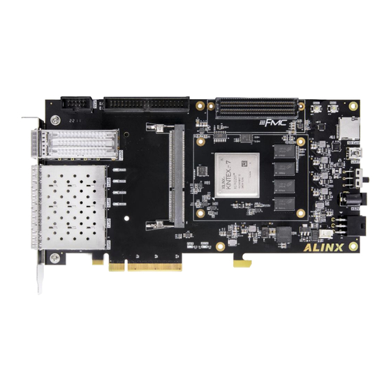
- Page 1 KINTEX-7 FPGA Development Board AX7325B User Manual...
-
Page 2: Version Record
KINTEX-7 FPGA Development Board AX7325B User Manual Version Record Version Date Release By Description Rev 1.1 2022-08-30 Rachel Zhou First Release www.alinx.com 2 / 49... -
Page 3: Table Of Contents
Part 14: Expansion Header ............... 39 Part 15: LED Light ..................41 Part16: User Buttons ................. 43 Part 17: JTAG Interface ................44 Part 18: Power Supply ................45 Part19: Fan ....................47 Part 20: Structure Diagram ................49 www.alinx.com 3 / 49... - Page 4 It is a "professional" FPGA development platform, for high-speed data transmission and exchange, pre-verification and post-application of data processing is possible. This product is very suitable for students, engineers and other groups engaged in KINTEX-7FPGA development. www.alinx.com 4 / 49...
-
Page 5: Part 1: Fpga Development Board Introduction
PCIex8 interface, four 10G optical SFP interfaces, one 40G optical fiber + QSFP interface, one UART serial interface, one SD card interface, and one FMC expansion interface. 1 40-pin expansion port and some button LEDs. www.alinx.com 5 / 49... - Page 6 A 128Mbit QSPI FLASH memory chip can be used as a storage for FPGA chip configuration files and user data; PCIe x8 interface A standard PCIEx8 interface for PCIE communication with computer motherboards, supports the PCI Express 2.0 standard, and www.alinx.com 6 / 49...
- Page 7 Onboard a temperature and humidity sensor chip LM75 for detecting the temperature and humidity of the environment around the board FMC expansion ports A standard FMC LPC expansion port can be connected to various FMC www.alinx.com 7 / 49...
-
Page 8: Part 2: Fpga Chip
KINTEX-7 FPGA Development Board AX7325B User Manual modules of XILINX or ALINX (HDMI input/output module, binocular camera module, high-speed AD module etc.) JTAG Interface A 10-pin0.1 spacing standard JTAG ports for FPGA program download and debugging. Users can debug and download FPGAs through XILINX downloader. - Page 9 FPGA core power supply pin, which needs to MGTAVCC MGTAVTT CCINT be connected to 1.0V; V is the power supply pin of FPGA Block RAM, CCBRAM connect to 1.0V; V is FPGA auxiliary power supply pin, connect 1.8V; V CCAUX www.alinx.com 9 / 49...
-
Page 10: Part 3:Ddr3 Dram
DDR3 memory systems are directly connected to the BANK32, BANK33, and BANK34 interfaces of the FPGA. The specific configuration of DDR3 SDRAM is shown in Table 3-1. Bit Number Chip Model Capacity Factory U3,U4,U6,U7 MT41K256M16HA-125 256M x 16bit Micron MT41J256M16HA-125 www.alinx.com 10 / 49... - Page 11 We have fully considered the matching resistor/terminal resistance, trace impedance control, and trace length control in circuit design and PCB design to ensure high-speed and stable operation of DDR3. Figure 3-1: The DDR3 DRAM Schematic www.alinx.com 11 / 49...
- Page 12 DDR3_D2 IO_L14P_T2_SRCC_32 AD17 DDR3_D3 IO_L17P_T2_32 AB19 DDR3_D4 IO_L14N_T2_SRCC_32 AD16 DDR3_D5 IO_L17N_T2_32 AC19 DDR3_D6 IO_L13N_T2_MRCC_32 AE18 DDR3_D7 IO_L18P_T2_32 AB17 DDR3_D8 IO_L8P_T1_32 AG19 DDR3_D9 IO_L7N_T1_32 AK19 DDR3_D10 IO_L10P_T1_32 AD19 DDR3_D11 IO_L7P_T1_32 AJ19 DDR3_D12 IO_L11P_T1_SRCC_32 AF18 DDR3_D13 IO_L8N_T1_32 AH19 www.alinx.com 12 / 49...
- Page 13 AA16 DDR3_D31 IO_L20N_T3_32 AB15 DDR3_D32 IO_L22N_T3_34 DDR3_D33 IO_L23P_T3_34 DDR3_D34 IO_L22P_T3_34 DDR3_D35 IO_L19P_T3_34 DDR3_D36 IO_L24N_T3_34 DDR3_D37 IO_L23N_T3_34 DDR3_D38 IO_L24P_T3_34 DDR3_D39 IO_L20N_T3_34 DDR3_D40 IO_L10P_T1_34 DDR3_D41 IO_L8N_T1_34 DDR3_D42 IO_L11P_T1_SRCC_34 DDR3_D43 IO_L8P_T1_34 DDR3_D44 IO_L12P_T1_MRCC_34 DDR3_D45 IO_L10N_T1_34 DDR3_D46 IO_L11N_T1_SRCC_34 DDR3_D47 IO_L7N_T1_34 www.alinx.com 13 / 49...
- Page 14 DDR3_DM3 IO_L24N_T3_32 DDR3_DM4 IO_L20P_T3_34 DDR3_DM5 IO_L7P_T1_34 DDR3_DM6 IO_L18P_T2_34 DDR3_DM7 IO_L1P_T0_34 DDR3_DQS0_P IO_L15P_T2_DQS_32 DDR3_DQS0_N IO_L15N_T2_DQS_32 DDR3_DQS1_P IO_L9P_T1_DQS_32 AJ18 DDR3_DQS1_N IO_L9N_T1_DQS_32 AK18 DDR3_DQS2_P IO_L3P_T0_DQS_32 AH16 DDR3_DQS2_N IO_L3N_T0_DQS_32 AJ16 DDR3_DQS3_P IO_L21P_T3_DQS_32 AC16 DDR3_DQS3_N IO_L21N_T3_DQS_32 AC15 DDR3_DQS4_P IO_L21P_T3_DQS_34 DDR3_DQS4_N IO_L21N_T3_DQS_34 www.alinx.com 14 / 49...
- Page 15 IO_L7N_T1_33 AC10 DDR3_A14 IO_L15P_T2_DQS_33 DDR3_BA0 IO_L8N_T1_33 DDR3_BA1 IO_L9P_T1_DQS_33 AC12 DDR3_BA2 IO_L9N_T1_DQS_33 AC11 DDR3_WE IO_L10P_T1_33 DDR3_RAS IO_L10N_T1_33 DDR3_CAS IO_L11P_T1_SRCC_33 AE11 DDR3_S0 IO_L11N_T1_SRCC_33 AF11 DDR3_CKE0 IO_L12P_T1_MRCC_33 AD12 DDR3_ODT IO_L12N_T1_MRCC_33 AD11 DDR3_CLK0_P IO_L13P_T2_MRCC_33 AG10 DDR3_CLK0_N IO_L13N_T2_MRCC_33 AH10 DDR3_RESET IO_L4P_T0_33 www.alinx.com 15 / 49...
-
Page 16: Part 4:Sodimm Memory Module Interface
Figure 4-1: SODIMM memory test sample The SODIMM memory module interface is directly connected to the interface of BANK16, BANK17 and BANK18 of FPGA. The hardware connection mode of FPGA and SODIMM DDR3 is shown in Figure 4-2. www.alinx.com 16 / 49... - Page 17 KINTEX-7 FPGA Development Board AX7325B User Manual Figure 4-2: SODIMM interface Connection Diagram Figure 4-3: SODIMM slot on the FPGA Board www.alinx.com 17 / 49...
- Page 18 DIMM_DDR3_D14 IO_L12P_T1_MRCC_18 DIMM_DDR3_D15 IO_L7N_T1_18 DIMM_DDR3_D16 IO_L13P_T2_MRCC_18 DIMM_DDR3_D17 IO_L17P_T2_18 DIMM_DDR3_D18 IO_L13N_T2_MRCC_18 DIMM_DDR3_D19 IO_L14N_T2_SRCC_18 DIMM_DDR3_D20 IO_L16P_T2_18 DIMM_DDR3_D21 IO_L16N_T2_18 DIMM_DDR3_D22 IO_L17N_T2_18 DIMM_DDR3_D23 IO_L14P_T2_SRCC_18 DIMM_DDR3_D24 IO_L22P_T3_18 DIMM_DDR3_D25 IO_L22N_T3_18 DIMM_DDR3_D26 IO_L23N_T3_18 DIMM_DDR3_D27 IO_L23P_T3_18 DIMM_DDR3_D28 IO_L24P_T3_18 DIMM_DDR3_D29 IO_L24N_T3_18 DIMM_DDR3_D30 IO_L20N_T3_18 DIMM_DDR3_D31 IO_L19P_T3_18 www.alinx.com 18 / 49...
- Page 19 DIMM_DDR3_D48 IO_L13P_T2_MRCC_16 DIMM_DDR3_D49 IO_L17N_T2_16 DIMM_DDR3_D50 IO_L16N_T2_16 DIMM_DDR3_D51 IO_L16P_T2_16 DIMM_DDR3_D52 IO_L13N_T2_MRCC_16 DIMM_DDR3_D53 IO_L17P_T2_16 DIMM_DDR3_D54 IO_L18P_T2_16 DIMM_DDR3_D55 IO_L14P_T2_SRCC_16 DIMM_DDR3_D56 IO_L20N_T3_16 DIMM_DDR3_D57 IO_L22N_T3_16 DIMM_DDR3_D58 IO_L24P_T3_16 DIMM_DDR3_D59 IO_L20P_T3_16 DIMM_DDR3_D60 IO_L19P_T3_16 DIMM_DDR3_D61 IO_L22P_T3_16 DIMM_DDR3_D62 IO_L23N_T3_16 DIMM_DDR3_D63 IO_L23P_T3_16 DIMM_DDR3_DM0 IO_L4P_T0_18 DIMM_DDR3_DM1 IO_L11P_T1_SRCC_18 www.alinx.com 19 / 49...
- Page 20 DIMM_DDR3_DQS5_P IO_L9P_T1_DQS_16 DIMM_DDR3_DQS5_N IO_L9N_T1_DQS_16 DIMM_DDR3_DQS6_P IO_L15P_T2_DQS_16 DIMM_DDR3_DQS6_N IO_L15N_T2_DQS_16 DIMM_DDR3_DQS7_P IO_L21P_T3_DQS_16 DIMM_DDR3_DQS7_N IO_L21N_T3_DQS_16 DIMM_DDR3_A0 IO_L11P_T1_SRCC_17 DIMM_DDR3_A1 IO_L8P_T1_17 DIMM_DDR3_A2 IO_L11N_T1_SRCC_17 DIMM_DDR3_A3 IO_L16N_T2_17 DIMM_DDR3_A4 IO_L3N_T0_DQS_17 DIMM_DDR3_A5 IO_L17N_T2_17 DIMM_DDR3_A6 IO_L4P_T0_17 DIMM_DDR3_A7 IO_L17P_T2_17 DIMM_DDR3_A8 IO_L1N_T0_17 DIMM_DDR3_A9 IO_L15N_T2_DQS_17 DIMM_DDR3_A10 IO_L6P_T0_17 DIMM_DDR3_A11 IO_L16P_T2_17 www.alinx.com 20 / 49...
-
Page 21: Part 5: Qspi Flash
QSPI FLASH are shown in Table 5-1. Position Model Capacity Factory N25Q128 128M Bit Numonyx Table 5-1: QSPI FLASH Specification QSPI FLASH is connected to the dedicated pins of BANK0 and BANK14 of www.alinx.com 21 / 49... - Page 22 Figure 5-1: QSPI Flash Schematic Figure 5-2: QSPI Flash on the FPGA Board QSPI Flash pin assignments: Signal Name FPGA Pin Name FPGA Pin Number FPGA_CCLK CCLK_0 FLASH_CE_B IO_L6P_T0_FCS_B_14 FLASH_D0 IO_L1P_T0_D00_MOSI_14 FLASH_D1 IO_L1N_T0_D01_DIN_14 FLASH_D2 IO_L2P_T0_D02_14 FLASH_D3 IO_L2N_T0_D03_14 www.alinx.com 22 / 49...
-
Page 23: Part 6: Clock Configuration
The schematic diagram of clock circuit design is shown in Figure 6-1 below: Figure 6-1: Programmable Clock Source Schematic Programmable Clock Source FPGA pin assignments: Signal Name FPGA Pin SYS_CLK_P AE10 SYS_CLK_N AF10 CLK0_P www.alinx.com 23 / 49... -
Page 24: Part7: Usb To Serial Port
USB port of the upper PC for serial data communication on the FPGA development board with a USB cable. The schematic diagram of the USB Uart circuit design is shown below: Figure 7-1: USB to serial port schematic www.alinx.com 24 / 49... -
Page 25: Part 8: Sfp Interface
FPGA and the optical module through a DC blocking capacitor in a differential signal mode. Each TX transmit and RX receive data rate is up to 10Gb/s. The BANK117's GTX transceiver reference clock is provided by the 156.25Mhz System Clock. www.alinx.com 25 / 49... - Page 26 KINTEX-7 FPGA Development Board AX7325B User Manual Figure 8-1: Optical Fiber Design Schematic Figure 8-2: SFP interfaces on the FPGA Board The 1 fiber interface FPGA pin assignment is as follows: Signal Name FPGA PIN Description SFP1_TX_P SFP1 Data Transfer (Positive) www.alinx.com 26 / 49...
- Page 27 SFP4 Data Transfer (Positive) SFP4_TX_N SFP4 Data Transfer (Negative) SFP4_RX_P SFP4 Data Receiver (Positive) SFP4_RX_P SFP4 Data Receiver (Negative) SFP4_TX_DIS SFP4 Optical Transfer Disable, active high SFP4_LOSS SFP4 Optical LOSS,High level means no light signal is received www.alinx.com 27 / 49...
-
Page 28: Part 9: Qsfp+ Fiber Interface
The QSFP+ fiber design diagram of the FPGA development board is shown in Figure 9-1, where the control signal of the fiber is connected to the BANK14 of the FPGA. Figure 9-1: QSFP+ Fiber Design Diagram www.alinx.com 28 / 49... - Page 29 QSFP + 4 Channel Data Send Negative QSFP_MODSELL Mode selection, low level I2C is valid QSFP_RESETL Reset signal, low reset QSFP_MODPRSL The optical module has a signal and is active low. QSFP_INTL Interrupt Signal, Active Low www.alinx.com 29 / 49...
-
Page 30: Part 10: Pcie Slot
5Gbps. The design diagram of the PCIe interface of the AX7325B FPGA development board is shown in Figure 10-1, where the TX transmit signal and the reference clock CLK signal are connected in AC coupled mode. www.alinx.com 30 / 49... - Page 31 PCIE Channel 0 Data Receive Positive PCIE_RX0_N PCIE Channel 0 Data Receive Negative PCIE_RX1_P PCIE Channel 1 Data Receive Positive PCIE_RX1_N PCIE Channel 1 Data Receive Negative PCIE_RX2_P PCIE Channel 2 Data Receive Positive PCIE_RX2_N PCIE Channel 2 Data Receive Negative www.alinx.com 31 / 49...
-
Page 32: Part 11: Temperature Sensor
AX7325B FPGA development board, and the model is LM75 of ON Semiconductor. The temperature accuracy of the LM75 chip is 0.5 degrees. The sensor and FPGA are directly connected to the I2C digital interface. The FPGA reads the temperature near the current FPGA development board www.alinx.com 32 / 49... -
Page 33: Part 12: Sd Card Slot
Figure 11-2: LM75 Sensor on the FPGA Board LM75 Sensor Pin Assignment Pin Name FPGA Pin LM75_SCL LM75_SDA Part 12: SD Card Slot The SD card (Secure Digital Memory Card) is a memory card based on the semiconductor flash memory process. It was www.alinx.com 33 / 49... - Page 34 +2.5V. However, the SD card has a data level of 3.3 and needs to be connected via the TXS02612 level shifter. The schematic diagram of the FPGA and SD card connector is shown in Figure 12-1. Figure 12-1: SD Card Slot Schematic www.alinx.com 34 / 49...
-
Page 35: Part 13: Fmc Connector
The AX7325B development board comes with a standard FMC LPC expansion port that can be connected to various FMC modules of XILINX or ALINX (HDMI input and output modules, binocular camera modules, high-speed AD modules, etc.). The FMC expansion port contains 34 pairs of differential IO signals and one I2C bus signal. - Page 36 BANK. The default is +2.5V. The 34 pairs of differential signals connected to the FMC support LVDS data communication. The schematic of the FPGA and FMC connectors is shown in Figure 13-1: Figure 13-1:FMC Connector diagram Figure 13-2:FMC Connector on the FPGA Board FMC Connectors Pin Assignment www.alinx.com 36 / 49...
- Page 37 FMC_LA11_P IO_L3P_T0_DQS_12 AB22 FMC reference 11 channel data P FMC_LA11_N IO_L3N_T0_DQS_12 AB23 FMC reference 11 channel data N FMC_LA12_P IO_L7P_T1_12 AB24 FMC reference 12 channel data P FMC_LA12_N IO_L7N_T1_12 AC25 FMC reference 12 channel data N www.alinx.com 37 / 49...
- Page 38 N FMC_LA27_P IO_L1P_T0_13 FMC reference 27 channel data P FMC_LA27_N IO_L1N_T0_13 AA26 FMC reference 27 channel data N FMC_LA28_P IO_L7P_T1_13 AC29 FMC reference 28 channel data P FMC_LA28_N IO_L7N_T1_13 AC30 FMC reference 28 channel data N www.alinx.com 38 / 49...
-
Page 39: Part 14: Expansion Header
The AX7325B FPGA development board is reserved with one 0.1inch spacing standard 40-pin expansion headers J2, which is used to connect the ALINX modules or the external circuit designed by the user. The expansion port has 40 signals, of which 1-channel 5V power supply, 2-channel3.3 V power Do not directly connect the IO directly supply,3-channle ground and 34 IOs. - Page 40 KINTEX-7 FPGA Development Board AX7325B User Manual Figure 14-1: Expansion header J2 schematic Figure 14-2: Expansion header J2 on the FPGA Board J16 Expansion Header Pin Assignment J16 Pin Number FPGA Pin J16 Pin Number FPGA Pin +5V(Output) www.alinx.com 40 / 49...
-
Page 41: Part 15: Led Light
LED will be extinguished.Because the level of BANK17 is 1.5V, here we have added a three-stage tube to drive the LED to light up.The LEDs hardware connection is shown in Figure 15-1. www.alinx.com 41 / 49... - Page 42 Figure 15-1: The LED lights hardware connection diagram Figure 15-2: The User LEDs on theFPGA Board Pin assignment of user LED lights Signal Name FPGA Pin FPGA Pin Number Description LED1 IO_L23N_T3_17 User LED1 LED2 IO_L24P_T3_17 User LED2 LED3 IO_L24N_T3_17 User LED3 www.alinx.com 42 / 49...
-
Page 43: Part16: User Buttons
KEY1~KEY2. The button is active low. The circuit of user button part is shown in Figure 16-1. Figure 16-1: User ButtonsSchematic Figure 16-2: User Buttons on the FPGA Board UseButtons Pin Assignment Signal Name FPGA Pin FPGA Pin Description Number KEY1 IO_L21P_T3_DQS_13 AG27 User Buttons KEY1 Input www.alinx.com 43 / 49... -
Page 44: Part 17: Jtag Interface
The Figure 17-2 detailed the JTAG interface on the AX7325B FPGA development board. Users can connect the PC and JTAG interface to debug the FPGA through the USB downloader provided by us. Be careful not to hot swap when JTAG cable is plugged and unplugged. www.alinx.com 44 / 49... -
Page 45: Part 18: Power Supply
/ DC power chip ETA8156FT2G, and generates other power through the DCDC chip ETA1471FT2G. The VTT and VREF voltages of DDR3 and SODIMM are generated by the TPS51200 chip. The Power supply design diagramis shown in Figure 18-1. www.alinx.com 45 / 49... - Page 46 The functions of each power distribution are shown in the following table: Power Supply Function FPGA core voltage +1.0V FPGA Bank0,Bank14,Bank15,QSIP FLASH, Clock Crystal, +3.3V SD Card, SFP Optical Module Gigabit Ethernet, HDMI, USB +1.8V +1.5V DDR3, SODIMM, FPGA Bank33,Bank34,Bank35 VADJ(+2.5V) FPGA Bank12, Bank13, FMC www.alinx.com 46 / 49...
-
Page 47: Part19: Fan
MOSFET is turned on and the fan is working. If the IO level output is high, the fan stops. The fan design on the board is shown in Figure 19-1. Figure 19-1:Fan design in the schematic www.alinx.com 47 / 49... - Page 48 The fan has been screwed to the AX7325B FPGA development board before leaving the factory. The power of the fan is connected to the socket of J11. The red is positive and the black is negative. Figure 19-2:Fan on the FPGA Board www.alinx.com 48 / 49...
-
Page 49: Part 20: Structure Diagram
KINTEX-7 FPGA Development Board AX7325B User Manual Part 20: Structure Diagram Figure 20-1: Structure Diagram (Top View) www.alinx.com 49 / 49...
Need help?
Do you have a question about the KINTEX-7FPGA and is the answer not in the manual?
Questions and answers