Table of Contents
Advertisement
Quick Links
Advertisement
Table of Contents

Related Manuals for IEI Technology WAFER-JL-N5105


Summary of Contents for IEI Technology WAFER-JL-N5105
- Page 1 WAFER-JL-N5105 SBC WAFER-JL-N5105 CPU Card MODEL: WAFER-JL-N5105 3.5" SBC with Intel® 10nm Jasper Lake Celeron® N5105 Processor with Dual Displays, DDR4, Triple Intel® 2.5 GbE, USB3.2, M.2, SATA, COM, SoC, RoHS User Manual Page I Rev. 1.00 - March 25, 2022...
- Page 2 WAFER-JL-N5105 SBC Revision Date Version Changes March 25, 2022 1.00 Initial release Page II [MODEL NAME]...
- Page 3 WAFER-JL-N5105 SBC Copyright COPYRIGHT NOTICE The information in this document is subject to change without prior notice in order to improve reliability, design and function and does not represent a commitment on the part of the manufacturer. In no event will the manufacturer be liable for direct, indirect, special, incidental, or consequential damages arising out of the use or inability to use the product or documentation, even if advised of the possibility of such damages.
- Page 4 WAFER-JL-N5105 SBC Manual Conventions WARNING Warnings appear where overlooked details may cause damage to the equipment or result in personal injury. Warnings should be taken seriously. CAUTION Cautionary messages should be heeded to help reduce the chance of losing data or damaging the product.
-
Page 5: Table Of Contents
PTIONAL TEMS 3 CONNECTORS ......................12 3.1 P ..............13 ERIPHERAL NTERFACE ONNECTORS 3.1.1 WAFER-JL-N5105 Layout ................13 3.1.2 Peripheral Interface Connectors ..............13 3.1.3 External Interface Panel Connectors ............... 15 3.2 I ..............15 NTERNAL ERIPHERAL ONNECTORS 3.2.1 Clear CMOS Button ..................15 3.2.1 AT/ATX Power Mode Setting ................ - Page 6 WAFER-JL-N5105 SBC 3.2.11 Reset Button Connector .................. 28 3.2.12 RS-232 Serial Port Connector ............... 29 3.2.13 SATA 6Gb/s Drive Connector ................ 30 3.2.14 SATA Power Connector .................. 31 3.2.15 SMBus/I C Connector ..................32 3.2.16 SPI Flash Connector ..................33 3.2.17 USB 2.0 Connector ..................
- Page 7 WAFER-JL-N5105 SBC B ............................64 C PRODUCT DISPOSAL ....................64 D ERROR BEEP CODE ....................66 D.1 PEI B ..................... 67 ODES D.2 DXE B ....................67 ODES Page VII [MODEL NAME]...
- Page 8 WAFER-JL-N5105 SBC List of Figures Figure 1-1: WAFER-JL-N5105 ......................2 Figure 1-2: Connectors ........................3 Figure 1-3: Dimensions (mm) ......................4 Figure 1-4: Data Flow Diagram ...................... 5 Figure 3-1: Connector And Jumper Locations ................13 Figure 3-2: Clear CMOS Location ....................16 Figure 3-3: AT/ATX Power Mode Switch Locations ..............17...
- Page 9 WAFER-JL-N5105 SBC Figure 3-28: External DisplayPort Connector Location ............45 Figure 3-29: HDMI Connector Pinout Locations ................45 Figure 4-1: SO-DIMM Installation ....................49 Figure 4-2: Inserting The M.2 Module Into The Slot At An Angle ..........50 Figure 4-3: Securing The M.2 Module ..................50 Figure 4-4: Heat Sink Retention Screws..................51...
- Page 10 WAFER-JL-N5105 SBC List of Tables Table 1-1: Technical Specifications ....................7 Table 2-1: Packing List .........................10 Table 2-2: Optional Items ......................11 Table 3-1: Peripheral Interface Connectors ................14 Table 3-2: Rear Panel Connectors ....................15 Table 3-3: Clear CMOS Pinouts ....................16 Table 3-4: AT/ATX Power Mode Switch Pinouts ................17 Table 3-5: ME Override Setting Jumper Pinouts ...............18...
- Page 11 WAFER-JL-N5105 SBC Table 3-29: External Display Port Connector Pinouts ..............44 Table 3-30: HDMI Connector Pinouts ..................45 Page XI [MODEL NAME]...
-
Page 13: Introduction
WAFER-JL-N5105 SBC Chapter Introduction Page 1... -
Page 14: Ntroduction
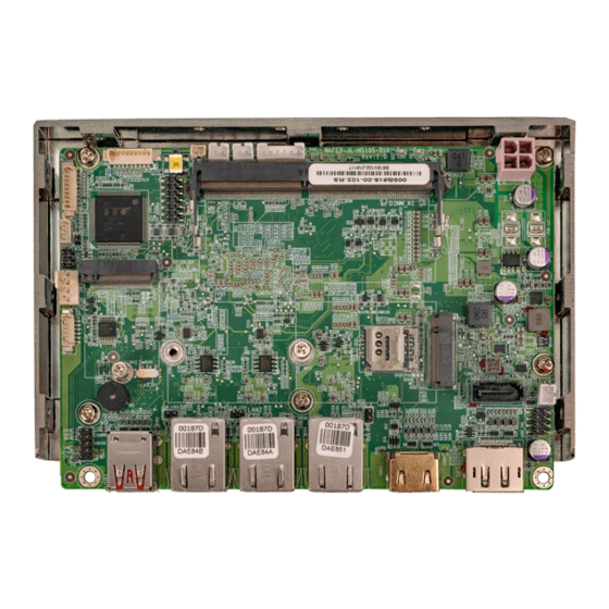
1.1 Introduction Figure 1-1: WAFER-JL-N5105 The WAFER-JL-N5105 is a 3.5" industrial motherboard equipped with an Intel® Celeron® N5105 quad-core Jasper Lake processor supporting 4 cores, 4 threads, turbo up-to 2.60 GHz with L3 cache, and supports one 260-pin 2933 MHz dual-channel DDR4 SDRAM SO- DIMM slot with up to 16 GB of memory. -
Page 15: Features
Two USB 3.2 Gen 2, two USB 2.0, two RS-232 M.2 A key and M.2 B key expansions Support dual independent display via HDMI and DP 1.3 Connectors The connectors on the WAFER-JL-N5105 are shown in the figure below. Figure 1-2: Connectors Page 3... -
Page 16: Dimensions
WAFER-JL-N5105 SBC 1.4 Dimensions The dimensions of the board are listed below: Figure 1-3: Dimensions (mm) Page 4... -
Page 17: Data Flow
WAFER-JL-N5105 SBC 1.5 Data Flow Shows the data flow between the system chipset, the CPU and other components installed on the motherboard. Figure 1-4: Data Flow Diagram Page 5... -
Page 18: Technical Specifications
WAFER-JL-N5105 SBC 1.6 Technical Specifications WAFER-JL-N5105 technical specifications are listed below. Specification WAFER-JL-N5105 Intel® Celeron® N5105 on-board SoC (up to 2.90GHz, Quad- core, 4M Cache, TDP=10W) BIOS AMI UEFI BIOS Memory One 260-pin 2933 MHz dual-channel DDR4 SO-DIMM (system max. 16GB) Graphics ®... -
Page 19: Table 1-1: Technical Specifications
WAFER-JL-N5105 SBC Specification WAFER-JL-N5105 Expansions 1 x M.2 2230 A key (PCIe Gen3 x1, USB 2.0) 1 x M.2 3042/2280 B key w/ SIM holder (PCIe Gen3 x2, USB 2.0) Environmental and Power Specifications Power Supply 12 V DC input only (AT/ATX support) -
Page 20: Unpacking
WAFER-JL-N5105 SBC Chapter Unpacking Page 8... -
Page 21: Anti-Static Precautions
Only handle the edges of the PCB: Don't touch the surface of the motherboard. Hold the motherboard by the edges when handling. 2.2 Unpacking Precautions When the WAFER-JL-N5105 is unpacked, please do the following: Follow the antistatic guidelines above. -
Page 22: Packing List
If any of the components listed in the checklist below are missing, do not proceed with the installation. Contact the IEI reseller or vendor the WAFER-JL-N5105 was purchased from or contact an IEI sales representative directly by sending an email to sales@ieiworld.com. -
Page 23: Optional Items
WAFER-JL-N5105 SBC 2.4 Optional Items The following are optional components which may be separately purchased: Item and Part Number Image Dual-port USB 2.0 cable, 210mm, P=2.0 (P/N : CB-USB02A-RS) RS-232 cable, 250 mm, p=1.25 (P/N : 32005-003500-200-RS) Audio kit, 7.1 Channel... -
Page 24: Connectors
WAFER-JL-N5105 SBC Chapter Connectors Page 12... -
Page 25: Peripheral Interface Connectors
WAFER-JL-N5105 SBC 3.1 Peripheral Interface Connectors This chapter details all the jumpers and connectors. 3.1.1 WAFER-JL-N5105 Layout The figures below show all the connectors and jumpers. Figure 3-1: Connector And Jumper Locations 3.1.2 Peripheral Interface Connectors The table below lists all the connectors on the board. -
Page 26: Table 3-1: Peripheral Interface Connectors
WAFER-JL-N5105 SBC Connector Type Label Clear CMOS button Button J_CMOS1 AT/ATX power mode setting 3-pin header J_ATX_AT1 ME override setting jumper 2-pin header ME_FLASH1 Internal audio connector 10-pin header AUDIO1 ATX 12V power connector 4-pin Molex PWR1 Digital I/O connector... -
Page 27: External Interface Panel Connectors
External DisplayPort connector External HDMI connector HDMI HDMI1 Table 3-2: Rear Panel Connectors 3.2 Internal Peripheral Connectors The section describes all of the connectors on the WAFER-JL-N5105. 3.2.1 Clear CMOS Button CN Label: J_CMOS1 CN Type: Button CN Location:... -
Page 28: Figure 3-2: Clear Cmos Location
WAFER-JL-N5105 SBC Figure 3-2: Clear CMOS Location PIN NO. DESCRIPTION Keep CMOS Setup NC (default) (Normal Operation) Press button Clear CMOS Setup Table 3-3: Clear CMOS Pinouts Page 16... -
Page 29: At/Atx Power Mode Setting
WAFER-JL-N5105 SBC 3.2.1 AT/ATX Power Mode Setting CN Label: J_ATX_AT1 CN Type: 3-pin switch CN Location: Figure 3-3 787H CN Pinouts: See Table 3-4 The AT/ATX power mode selection is made through the AT/ATX power mode switch which is shown in Figure3-3. -
Page 30: Figure 3-4: Me Override Setting Jumper Locations
WAFER-JL-N5105 SBC Figure 3-4: ME Override Setting Jumper Locations PIN NO. DESCRIPTION Open Disable (default) Short Enable Table 3-5: ME Override Setting Jumper Pinouts To update the ME firmware, please follow the steps below. Step 1: Before turning on the system power, short the Flash Descriptor Security Override jumper. -
Page 31: Audio Connector
WAFER-JL-N5105 SBC 3.2.3 Audio Connector CN Label: AUDIO1 CN Type: 10-pin header, p=2.00 mm CN Location: See Figure 3-5 CN Pinouts: See Table 3-6 The audio connector is connected to external audio devices (AC-KIT-888S-R10) including speakers and microphones for the input and output of audio signals to and from the system. -
Page 32: Atx 12V Power Connector
WAFER-JL-N5105 SBC 3.2.4 ATX 12V Power Connector CN Label: PWR1 CN Type: 4-pin Molex, p=4.2 mm CN Location: See Figure 3-6 CN Pinouts: See Table 3-7 The connector supports the +12V power supply. Figure 3-6: ATX 12V Power Connector Location PIN NO. -
Page 33: Figure 3-7: Digital I/O Connector Location
WAFER-JL-N5105 SBC The 12-bit digital I/O connector provides programmable input and output for external devices. Figure 3-7: Digital I/O Connector Location PIN NO. DESCRIPTION PIN NO. DESCRIPTION DOUT5 DOUT4 DOUT3 DOUT2 DOUT1 DOUT0 DIN5 DIN4 DIN3 DIN2 DIN1 DIN0 Table 3-8: Digital I/O Connector Pinouts... -
Page 34: Fan Connector
WAFER-JL-N5105 SBC 3.2.6 Fan Connector CN Label: CPU_FAN1 CN Type: 4-pin wafer, p=2.54 mm CN Location: See Figure 3-8 CN Pinouts: See Table 3-9 The fan connector attaches to a smart cooling fan. Figure 3-8: Fan Connector Location Description Description... -
Page 35: Power Led & Hdd Led Connector
WAFER-JL-N5105 SBC 3.2.7 Power LED & HDD LED Connector CN Label: F_PANEL1 CN Type: 6-pin wafer, p=2.00 mm CN Location: See Figure 3-9 CN Pinouts: See Table 3-10 The front panel connector connects to the power LED indicator and HDD LED indicator on the system front panel. -
Page 36: Lan Led Connectors
WAFER-JL-N5105 SBC 3.2.8 LAN LED Connectors CN Label: JLAN_LED1, JLAN_LED2, JLAN_LED3 CN Type: 2-pin header, p=2.00 mm CN Location: See Figure 3-10 CN Pinouts: See Table 3-11, Table 3-12 and Table 3-13 The LAN LED connectors connect to the LAN link LEDs on the system. -
Page 37: Battery Connector
Dispose of used batteries according to instructions and local regulations. NOTE: It is recommended to attach the RTC battery onto the system chassis in which the WAFER-JL-N5105 is installed. CN Label: BAT2 CN Type: 2-pin wafer, p=1.25 mm... -
Page 38: Figure 3-11: Battery Connector Location
WAFER-JL-N5105 SBC Figure 3-11: Battery Connector Location Description VBAT+ Table 3-14: Battery Connector Pinouts Page 26... -
Page 39: Power Button Connector
WAFER-JL-N5105 SBC 3.2.10 Power Button Connector CN Label: PWR_BTN1 CN Type: 2-pin wafer, p=2.00 mm CN Location: See Figure 3-12 CN Pinouts: See Table 3-15 The power button connector is connected to a power switch on the system chassis to enable users to turn the system on and off. -
Page 40: Reset Button Connector
WAFER-JL-N5105 SBC 3.2.11 Reset Button Connector CN Label: RST_BTN1 CN Type: 2-pin wafer, p=2.00 mm CN Location: See Figure 3-13 CN Pinouts: See Table 3-16 The reset button connector is connected to a reset switch on the system chassis to enable users to reboot the system when the system is turned on. -
Page 41: Rs-232 Serial Port Connector
WAFER-JL-N5105 SBC 3.2.12 RS-232 Serial Port Connector CN Label: COM1,COM2 CN Type: 9-pin wafer, p=1.25 mm CN Location: See Figure 3-14 CN Pinouts: See Table 3-17 The serial connector provides RS-232 connection. Figure 3-14: RS-232 Serial Port Connector Location PIN NO. -
Page 42: Sata 6Gb/S Drive Connector
WAFER-JL-N5105 SBC 3.2.13 SATA 6Gb/s Drive Connector CN Label: SATA1 CN Type: 7-pin SATA connector CN Location: See Figure 3-15 CN Pinouts: See Table 3-18 The SATA 6Gb/s drive connector is connected to a SATA 6Gb/s drive. The SATA 6Gb/s drive transfers data at speeds as high as 6Gb/s. -
Page 43: Sata Power Connector
WAFER-JL-N5105 SBC 3.2.14 SATA Power Connector CN Label: SATA_PWR1 CN Type: 2-pin wafer, p=2.00 mm CN Location: See Figure 3-16 CN Pinouts: See Table 3-19 The SATA power connector provides +5 V power output to the SATA connector. Figure 3-16: SATA Power Connector Location... -
Page 44: Smbus/I C Connector
WAFER-JL-N5105 SBC 3.2.15 SMBus/I C Connector CN Label: I2C1 CN Type: 4-pin wafer, p=1.25 mm CN Location: See Figure 3-17 CN Pinouts: See Table 3-20 The SMBus (System Management Bus) connector provides low-speed system management communications. Figure 3-17: SMBus Connector Location... -
Page 45: Spi Flash Connector
WAFER-JL-N5105 SBC 3.2.16 SPI Flash Connector CN Label: JSPI1 CN Type: 6-pin wafer, p=1.25 mm CN Location: See Figure 3-18 CN Pinouts: See Table 3-21 The 6-pin SPI Flash connector is used to flash the BIOS. Figure 3-18: SPI Flash Connector Location Description +3.3V... -
Page 46: Usb 2.0 Connector
WAFER-JL-N5105 SBC 3.2.17 USB 2.0 Connector CN Label: USB3 CN Type: 8-pin header, p=2.00 mm CN Location: See Figure 3-19 CN Pinouts: See Table 3-22 The USB connector provides two USB 2.0 ports by dual-port USB cable. Figure 3-19: USB Connector Location PIN NO. -
Page 47: Slot, B-Key
WAFER-JL-N5105 SBC 3.2.18 M.2 Slot, B-key CN Label: M2_1 CN Type: M.2 B-key slot CN Location: Figure 3-20 791H CN Pinouts: See Table 3-23 The M.2 B key (3042/2280) slot with PCIe Gen3 x2 and USB 2.0 signal supports NVMe storage or 5G module with SIM holder Figure 3-20: M.2 B key Slot Location... -
Page 48: Table 3-23: M. 2 B Key Slot Pinouts
WAFER-JL-N5105 SBC GNSS_DISABLE PCIE_RXN1 UIM_RST PCIE_RXP1 UIM_CLK UIM_DATA PCIE_TXN1 UIM_VCC PCIE_TXP1 DEVSLP PCIE_RXN0 PCIE_RXP0 PCIE_TXN0 PCIE_TXP0 PERST# CLKREQ# REFCLKN PEWAKE REFCLKP WWAN_RST PEDET +3.3V +3.3V +3.3V CONFIG_2 Table 3-23: M. 2 B key Slot Pinouts Page 36... -
Page 49: Slot, A-Key
WAFER-JL-N5105 SBC 3.2.19 M.2 Slot, A-key CN Label: M2_A1 CN Type: M.2 A-key slot CN Location: See Figure 3-21 CN Pinouts: See Table 3-24 The M.2 slot is keyed in the A position and accepts 2230 size of M.2 modules. The M.2 slot supports PCIe x2 and USB 2.0 signals. -
Page 50: Table 3-24: M.2 A-Key Slot Pinouts
WAFER-JL-N5105 SBC Description Description PCIE_TX0+ PCIE_TX0- PCIE_RX0+ PCIE_RX0- CLK_PCIE0+ CLK_PCIE0- BUF_PLT_RST# PCIE_CLKREQ# Pull Up +V3.3A PCIE_WAKE# Pull Up +V3.3A PCIE_TX1+ PCIE_TX1- PCIE_RX1+ PCIE_RX1- CLK_PCIE1+ +V3.3A CLK_PCIE1- +V3.3A Table 3-24: M.2 A-Key Slot Pinouts Page 38... -
Page 51: Sim Slot
WAFER-JL-N5105 SBC 3.2.20 SIM Slot CN Label: SIM1 CN Type: 7-PIN SIM holder CN Location: See Figure 3-22 CN Pinouts: See Table 3-25 Figure 3-22: SIM Slot Location PIN NO. DESCRIPTION SIM_VCC SIM_RST SIM_Clock SIM_VPP SIM_DATA Table 3-25: SIM Slot Pinouts... -
Page 52: Ddr4 So-Dimm Socket
WAFER-JL-N5105 SBC 3.2.21 DDR4 SO-DIMM Socket CN Label: DIMM_A1 CN Type: 260-pin DDR4 SO-DIMM socket CN Location: Figure 3-23 791H The SO-DIMM slot is for installing the DDR4 SO-DIMM. Figure 3-23: DDR4 SO-DIMM Socket Location Page 40... -
Page 53: External Peripheral Interface Connector Panel
WAFER-JL-N5105 SBC 3.3 External Peripheral Interface Connector Panel Figure 3-24 shows the WAFER-JL-N5105 external peripheral interface connector (EPIC) panel. The EPIC panel consists of the following: 1x HDMI &1 x DP connector 3 x GbE RJ-45 connector ... -
Page 54: External 2.5Gbe Rj-45 Connectors
WAFER-JL-N5105 SBC 3.3.1 External 2.5GbE RJ-45 Connectors CN Label: LAN1, LAN2, LAN3 CN Type: RJ-45 CN Location: Figure 3-25 808H CN Pinouts: Table 3-26 809H The LAN connector connects to a local network. LAN LED location and pinouts see Figure 3-26 and Table 3-27. -
Page 55: External Usb 3.2 Gen 2X1 Type-A
CN Pinouts: Table 3-28 815H The WAFER-JL-N5105 has four external USB 3.2 Gen 2 ports. The USB connector can be connected to a USB 2.0 or USB 3.2 device. The pinouts of USB 3.2 Gen 2 connectors are shown below. -
Page 56: External Displayport Connector
WAFER-JL-N5105 SBC Description Description USB_DATA0- USB_DATA1- USB_DATA0+ USB_ DATA1+ USB3_RX0- USB3_RX1- USB3_RX0+ USB3_ RX1+ USB3_TX0- USB3_TX1- USB3_TX0+ USB3_TX1+ Table 3-28: USB 3.2 Gen 2 Port Pinouts 3.3.1 External DisplayPort Connector CN Label: CN Type: External DP connector CN Location: See Figure 3-28... -
Page 57: External Interface Panel Connectors
WAFER-JL-N5105 SBC Figure 3-28: External DisplayPort Connector Location 3.3.2 External Interface Panel Connectors CN Label: HDMI1 CN Type: HDMI connector CN Location: See Figure 3-29 CN Pinouts: See Table 3-30 The HDMI connectors can connect to HDMI devices. Description Description... -
Page 58: Installation
WAFER-JL-N5105 SBC Chapter Installation Page 46... -
Page 59: Anti-Static Precautions
Electrostatic discharge (ESD) can cause serious damage to electronic components, including the WAFER-JL-N5105. Dry climates are especially susceptible to ESD. It is therefore critical that whenever the WAFER-JL-N5105 or any other electrical component is handled, the following anti-static precautions are strictly adhered to. - Page 60 WAFER-JL-N5105 SBC WARNING: The installation instructions described in this manual should be carefully followed in order to prevent damage to the WAFER-JL-N5105, WAFER-JL- N5105 components and injury to the user. Before and during the installation please DO the following: ...
-
Page 61: So-Dimm Installation
WAFER-JL-N5105 SBC 4.3 SO-DIMM Installation To install an SO-DIMM, please follow the steps below and refer to Figure 4-1. Figure 4-1: SO-DIMM Installation Step 1: Locate the SO-DIMM socket. Place the board on an anti-static mat. Step 2: Align the SO-DIMM with the socket. Align the notch on the memory with the notch on the memory socket. -
Page 62: Module Installation
WAFER-JL-N5105 SBC 4.4 M.2 Module Installation To install an M.2 module, please follow the steps below. Step 1: Locate the M.2 module slot. See Chapter 3. Step 2: Remove the retention screw secured on the motherboard. Step 3: Line up the notch on the module with the notch on the slot. Slide the M.2 module into the socket at an angle of about 20º... -
Page 63: Chassis Installation
WAFER-JL-N5105 without the heat spreader secured to the board. When the WAFER-JL-N5105 is shipped, it is secured to a heat spreader with five retention screws. The heat spreader must have a direct contact with a heat dissipation surface to ensure stable operation. -
Page 64: Motherboard Installation
Figure 4-6: Passive Cooling 4.5.1 Motherboard Installation IEI recommend you to choose the DRPC-W-JL for the WAFER-JL-N5105 installation. The DRPC-W-JL is a compact embedded chassis designed for 3.5" single board computers. With its two-dimensional heat conduction and low wind resistance design on the surfaced, no extra thermal solution is needed to form the heat dissipation part. -
Page 65: Internal Peripheral Device Connections
WAFER-JL-N5105 SBC The WAFER-JL-N5105 is also well designed to fit into other chassis in the market. Each side of the heat spreader has several screw holes allowing the WAFER-JL-N5105 to be mounted into a chassis or a heat sink enclosure (please refer to Figure 1-3 for the detailed dimensions). -
Page 66: Figure 4-10: Power Cable To Motherboard Connection
WAFER-JL-N5105 SBC Step 2: Connect the power cable to the motherboard. Connect the 4-pin (2x2) Molex type power cable connector to the power connector on the motherboard. See Figure 4-10 Figure 4-10: Power Cable to Motherboard Connection Step 3: Connect power cable to power supply. Connect one of the 4-pin (1x4) Molex type power cable connectors to an AT power supply. -
Page 67: Channel Audio Kit Installation
WAFER-JL-N5105 SBC Figure 4-11: Connect Power Cable to Power Supply 4.6.2 7.1 Channel Audio Kit Installation NOTE: This item must be ordered separately, and connects to the audio connector. For further information please contact the nearest distributor, reseller or vendor or contact an IEI sales representative directly. -
Page 68: Rs-232 Cable Connection
WAFER-JL-N5105 SBC Figure 4-12: 7.1 Channel Audio Kit Step 3: Mount the audio kit onto the chassis. Once the audio kit is connected to the board, secure the audio kit bracket to the system chassis. Step 4: Connect the audio devices. Connect speakers and external audio sources to the audio jacks on the audio kit. -
Page 69: Sata Drive Connection
Step 0: system. 4.6.4 SATA Drive Connection The WAFER-JL-N5105 is shipped with a SATA drive cable. To connect the SATA drive to the connector, please follow the steps below. Step 1: Locate the SATA connector and the SATA power connector. The locations of the connectors are shown in Chapter 3. -
Page 70: Figure 4-14: Sata Drive Cable Connection
WAFER-JL-N5105 SBC Figure 4-14: SATA Drive Cable Connection Step 3: Connect the cable to the SATA disk. Connect the connector on the other end of the cable to the connector at the back of the SATA drive. Step 4: To remove the SATA cable from the SATA connector, press the clip on the Step 0: connector at the end of the cable. -
Page 71: Software Drivers
WAFER-JL-N5105 SBC Chapter Software Drivers Page 59... -
Page 72: Available Drivers
WAFER-JL-N5105 SBC 5.1 Available Drivers All the drivers for the WAFER-JL-N5105 are available on IEI Resource Download Center (https://download.ieiworld.com). Type WAFER-JL-N5105 and press Enter to find all the relevant software, utilities, and documentation. Figure 5-1: IEI Resource Download Center 5.2 Driver Download To download drivers from IEI Resource Download Center, follow the steps below. - Page 73 WAFER-JL-N5105 SBC Step 3: Click the driver file name on the page and you will be prompted with the following window. You can download the entire ISO file ( ), or click the small arrow to find an individual driver and click the file name to download (...
-
Page 74: A Regulatory Compliance
WAFER-JL-N5105 SBC Appendix Regulatory Compliance Page 62... - Page 75 WAFER-JL-N5105 SBC DECLARATION OF CONFORMITY This equipment has been tested and found to comply with specifications for CE marking. If the user modifies and/or installs other devices in the equipment, the CE conformity declaration may no longer apply. FCC WARNING This equipment complies with Part 15 of the FCC Rules.
-
Page 76: C Product Disposal
WAFER-JL-N5105 SBC Appendix Product Disposal Page 64... - Page 77 WAFER-JL-N5105 SBC CAUTION: Risk of explosion if battery is replaced by an incorrect type. Only certified engineers should replace the on-board battery. Dispose of used batteries according to instructions and local regulations. Outside the European Union–If you wish to dispose of used electrical and electronic products outside the European Union, please contact your local authority so as to comply with the correct disposal method.
-
Page 78: D Error Beep Code
WAFER-JL-N5105 SBC Appendix Error Beep Code Page 66... -
Page 79: Pei Beep Codes
WAFER-JL-N5105 SBC D.1 PEI Beep Codes Number of Beeps Description Memory not Installed Memory was installed twice (InstallPeiMemory routine in PEI Core called twice) Recovery started DXEIPL was not found DXE Core Firmware Volume was not found Recovery failed S3 Resume failed Reset PPI is not available D.2 DXE Beep Codes...
Need help?
Do you have a question about the WAFER-JL-N5105 and is the answer not in the manual?
Questions and answers