Advertisement
Quick Links
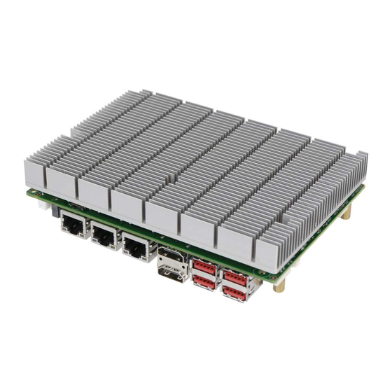
3.5" SBC supports 14nm 8th Gen. Intel
on-board Processor (ULT, 15W) with DDR4 SO-DIMM, Triple Display
by Dual HDMI & LVDS, M.2 A-key, PCIe Mini with mSATA,
USB 3.2 Gen 2 (10Gb/s), SATA 6Gb/s, Dual COM, Audio and RoHS
Quick Installation Guide
Package List
WAFER-ULT5 package includes the following items:
1 x WAFER-ULT5 single board computer with heat spreader
1 x Power cable
1 x RS-232/422/485 cable
1 x SATA and power cable
1 x QIG (Quick Installation Guide)
WAFER-ULT5
Version 1.0
November 6, 2019
©2019 Copyright by IEI Integration Corp.
All rights reserved.
®
Core™ i7/i5/i3 or Celeron
®
Advertisement

Related Manuals for IEI Technology WAFER-ULT5


Summary of Contents for IEI Technology WAFER-ULT5
- Page 1 WAFER-ULT5 Quick Installation Guide Version 1.0 November 6, 2019 Package List WAFER-ULT5 package includes the following items: 1 x WAFER-ULT5 single board computer with heat spreader 1 x Power cable 1 x RS-232/422/485 cable 1 x SATA and power cable ...
-
Page 2: Specifications
Specifications SoC: generation Intel® mobile ULT on-board SoC Intel® Core™ i7-8665UE Processor Intel® Core™ i5-8365UE Processor Intel® Core™ i3-8145UE Processor Intel® Celeron® Processor 4305UE Intel® Celeron® Processor 4205UE BIOS: AMI UEFI BIOS Memory: One 260-pin 2400 MHz DDR4 SO-DIMM slot (system max. - Page 3 1 x SATA 6G/s with 5V SATA power connector SMBus/I C: one via 4-pin wafer (1x4) Audio: 1 x Analog audio (2x5 pin) Front Panel: 1 x Power LED & HDD LED (1x6 pin) 1 x Power button (1x2 pin) 1 x Reset button (1x2 pin) ...
-
Page 4: Ordering Information
WAFER-ULT5 are available on IEI https://download.ieiworld.com Resource Download Center. Type WAFER-ULT5 and press Enter to find all the relevant software, utilities, and documentation. To install software from the downloaded ISO file, mount the file as a virtual drive to view its content. -
Page 5: Jumpers Setting And Connectors
Jumpers setting and connectors LABEL FUNCTION J_ATX_AT1 Power mode switch J_CMOS1 Clear CMOS button LVDS voltage selection jumper ME_FLASH1 ME override jumper HDMI1 External dual HDMI connector LAN1, LAN2, LAN3 GbE RJ-45 connectors USB1, USB2 External USB 3.2 Gen 2 connectors J_AUDIO1 Audio connector BAT1... - Page 6 J_ATX_AT1: Power Mode Switch PIN NO. DESCRIPTION Short A - B ATX Power Mode (Default) Short B - C AT Power Mode J_CMOS1: Clear CMOS Button PIN NO. DESCRIPTION Open Normal Operation (Default) Push Clear CMOS Setup JP1: LVDS Voltage Selection PIN NO.
- Page 7 HDMI1: HDMI Connectors PIN NO. DESCRIPTION PIN NO. DESCRIPTION HDMI_A_DATA2P HDMI_B_DATA2P HDMI_A_DATA2N HDMI_B_DATA2N HDMI_A_DATA1P HDMI_B_DATA1P HDMI_A_DATA1N HDMI_B_DATA1N HDMI_A_DATA0P HDMI_B_DATA0P HDMI_A_DATA0N HDMI_B_DATA0N HDMI_A_CLKP HDMI_B_CLKP HDMI_A_CLKN HDMI_B_CLKN HDMI_A_SCL HDMI_B_SCL HDMI_A_SDA HDMI_B_SDA USB1, USB2: External USB 3.2 Gen 2 (10Gb/s) Connectors PIN NO. DESCRIPTION PIN NO.
- Page 8 J_AUDIO1: Audio Connector PIN NO. DESCRIPTION PIN NO. DESCRIPTION HAD_BCLK HDA_SYNC HDA_SDO HDA_PCBEEP HAD_SDI0 HDA_RST# +12V BAT1: BAT Connector PIN NO. DESCRIPTION PIN NO. DESCRIPTION VBATT DIO1: Digital Input / Output Connector PIN NO. DESCRIPTION PIN NO. DESCRIPTION Output 3 Output 2 Output 1 Output 0...
- Page 9 LVDS1: LVDS Connector PIN NO. DESCRIPTION PIN NO. DESCRIPTION GROUND GROUND LVDS_A_TX0-N LVDS_A_TX1-N LVDS_A_TX0-P LVDS_A_TX1-P GROUND GROUND LVDS_A_TX2-N LVDS_A_TXCLK-N LVDS_A_TX2-P LVDS_A_TXCLK-P GROUND GROUND LVDS_A_TX3-N LVDS_B_TX0-N LVDS_A_TX3-P LVDS_B_TX0-P GROUND GROUND LVDS_B_TX1-N LVDS_B_TX2-N LVDS_B_TX1-P LVDS_B_TX2-P GROUND GROUND LVDS_B_TXCLK-N LVDS_B_TX3-N LVDS_B_TXCLK-P LVDS_B_TX3-P GROUND GROUND GROUND GROUND...
- Page 10 PWR2: +12V Power Connector PIN NO. DESCRIPTION PIN NO. DESCRIPTION +12V +12V RST_BTN1: Reset Button Connector PIN NO. DESCRIPTION PIN NO. DESCRIPTION RESET+ RESET- COM1: Internal RS-232/422/485 Serial Port Connector PIN NO. RS-232 RS-422 RS-485 TXD- DATA- TXD+ DATA+ RXD+ RXD- COM2: Internal RS-232 Serial Port Connector PIN NO.
- Page 11 SATA1: Serial ATA Connector PIN NO. DESCRIPTION PIN NO. DESCRIPTION SATA_PWR1: SATA Power Connector PIN NO. DESCRIPTION PIN NO. DESCRIPTION SMB1: SMBus Connector PIN NO. DESCRIPTION PIN NO. DESCRIPTION SMBUS (I C) DATA SMBUS (I C) CLOCK CPU/FAN1: Smart Fan Connector PIN NO.
- Page 12 MINI_PCIE1: PCIe Mini Card Slot (Full-Size) PIN NO. DESCRIPTION PIN NO. DESCRIPTION PCIE_WAKE# VCC3 1.5V PCIE_CLK# PCIE_CLK PCIRST# PCIE_RXN PCIE_RXP 1.5V SMBCLK PCIE_TXN SMBDATA PCIE_TXP USBD- USBD+ VCC3 VCC3 1.5V VCC3...
- Page 13 M2_A1: M.2 2230 A-key Slot PIN NO. DESCRIPTION PIN NO. DESCRIPTION +V3.3A USB+ +V3.3A USB- Module Key Module Key Module Key Module Key Module Key Module Key Module Key Module Key PCIE_TX0+ PCIE_TX0- PCIE_RX0+ PCIE_RX0- CLK_PCIE0+ CLK_PCIE0- BUF_PLT_RST# PCIE_CLKREQ# Pull Up +V3.3A PCIE_WAKE# Pull Up +V3.3A PCIE_TX1+...
- Page 14 Board Layout: Jumper and Connector Locations (Unit: mm)
Need help?
Do you have a question about the WAFER-ULT5 and is the answer not in the manual?
Questions and answers