Table of Contents
Advertisement
Quick Links
Advertisement
Table of Contents

Related Manuals for IEI Technology WAFER-CV-D25501 Series


Summary of Contents for IEI Technology WAFER-CV-D25501 Series
- Page 1 WAFER-CV-D25501/N26001 3.5" SBC MODEL: WAFER-CV-D25501/N26001 3.5" SBC with Intel® Atom™ D2550/N2600 Processor, DDR3, VGA/Dual LVDS, Dual PCIe GbE, USB 2.0, PCIe Mini, SATA 3Gb/s, Audio and RoHS User Manual Page i Rev. 1.05 – October 26, 2017...
- Page 2 WAFER-CV-D25501/N26001 3.5" SBC Revision Date Version Changes 1.05 Modified Figure 3-22: RJ-45 Ethernet Connector October 26, 2017 1.04 Updated Section 1.4: Dimensions August 27, 2015 Updated Section 4.5: Chassis Installation 1.03 Added CN6 connector information December 11, 2012 1.02 Updated the note for the Intel® GMA driver limitation 23 November, 2012 1.01 Added a note for the Intel®...
- Page 3 WAFER-CV-D25501/N26001 3.5" SBC Copyright COPYRIGHT NOTICE The information in this document is subject to change without prior notice in order to improve reliability, design and function and does not represent a commitment on the part of the manufacturer. In no event will the manufacturer be liable for direct, indirect, special, incidental, or consequential damages arising out of the use or inability to use the product or documentation, even if advised of the possibility of such damages.
- Page 4 WAFER-CV-D25501/N26001 3.5" SBC Manual Conventions WARNING Warnings appear where overlooked details may cause damage to the equipment or result in personal injury. Warnings should be taken seriously. CAUTION Cautionary messages should be heeded to help reduce the chance of losing data or damaging the product. NOTE These messages inform the reader of essential but non-critical information.
-
Page 5: Table Of Contents
WAFER-CV-D25501/N26001 3.5" SBC Table of Contents 1 INTRODUCTION......................1 1.1 I ......................2 NTRODUCTION 1.2 M ....................2 ODEL ARIATIONS 1.3 C ......................3 ONNECTORS 1.4 D ....................... 4 IMENSIONS 1.5 D ........................ 6 1.6 T ..................7 ECHNICAL PECIFICATIONS 2 PACKING LIST ...................... - Page 6 WAFER-CV-D25501/N26001 3.5" SBC 3.2.11 LVDS2 Backlight Control Connector ............. 26 3.2.12 PCIe Mini Card Slots..................26 3.2.13 Power & HDD LED Connector..............28 3.2.14 Power Button Connector................29 3.2.15 Reset Button Connector ................. 30 3.2.16 RS-232 Serial Port Connectors..............30 3.2.17 RS-422/485 Serial Port Connector ..............
- Page 7 WAFER-CV-D25501/N26001 3.5" SBC 4.6.7 Keyboard/Mouse Y-cable Connector ............... 58 5 BIOS ..........................61 5.1 I ......................62 NTRODUCTION 5.1.1 Starting Setup....................62 5.1.2 Using Setup ...................... 62 5.1.3 Getting Help..................... 63 5.1.4 Unable to Reboot after Configuration Changes ..........63 5.1.5 BIOS Menu Bar....................
- Page 8 WAFER-CV-D25501/N26001 3.5" SBC 6.5 LAN D ..................99 RIVER NSTALLATION 6.6 A ................101 UDIO RIVER NSTALLATION A REGULATORY COMPLIANCE ................104 B BIOS OPTIONS ......................106 C TERMINOLOGY ..................... 109 D DIGITAL I/O INTERFACE..................113 D.1 I .......................114 NTRODUCTION D.2 A 1................115 SSEMBLY ANGUAGE...
- Page 9 WAFER-CV-D25501/N26001 3.5" SBC List of Figures Figure 1-1: WAFER-CV-D25501/N26001 ..................2 Figure 1-2: Connectors ........................3 Figure 1-3: WAFER-CV-D25501/N26001 Dimensions (mm) ............5 Figure 1-4: Data Flow Diagram......................6 Figure 3-1: Connectors and Jumpers..................14 Figure 3-2: 5 V SATA Power Connector Locations ..............16 Figure 3-3: 12 V Power Connector Location................17 Figure 3-4: Audio Connector Location ..................18 Figure 3-5: Backlight Inverter Connector Locations..............19 Figure 3-6: Battery Connector Location..................20...
- Page 10 WAFER-CV-D25501/N26001 3.5" SBC Figure 4-3: Clear CMOS Jumper Location .................44 Figure 4-4: LVDS1 Voltage Selection Jumper Location ............45 Figure 4-5: LVDS2 Voltage Selection Jumper Location ............46 Figure 4-6: LVDS2 Panel Type Selection Switch Location............47 Figure 4-7: Heat Sink Retention Screws ..................48 Figure 4-8: Motherboard Installation Example ................49 Figure 4-9: Audio Kit Cable Connection..................50 Figure 4-10: LVDS Connector......................52...
- Page 11 WAFER-CV-D25501/N26001 3.5" SBC Figure 6-18: Audio Driver Installation Complete ..............103 Page xi...
- Page 12 WAFER-CV-D25501/N26001 3.5" SBC List of Tables Table 1-1: WAFER-CV-D25501/N26001 Model Variations ............2 Table 1-2: WAFER-CV-D25501/N26001 Specifications ...............8 Table 2-1: Packing List.........................12 Table 2-2: Optional Items......................12 Table 3-1: Peripheral Interface Connectors ................15 Table 3-2: Rear Panel Connectors ....................16 Table 3-3: 5 V SATA Power Connector Pinouts ................17 Table 3-4: 12 V Power Connector Pinouts .................17 Table 3-5: Audio Connector Pinouts ..................18 Table 3-6: Backlight Inverter Connector Pinouts ..............19...
- Page 13 WAFER-CV-D25501/N26001 3.5" SBC Table 4-1: Jumpers ........................42 Table 4-2: AT/ATX Power Selection Jumper Settings...............43 Table 4-3: Clear CMOS Jumper Settings..................43 Table 4-4: LVDS1 Voltage Selection Jumper Settings..............44 Table 4-5: LVDS2 Voltage Selection Jumper Settings..............45 Table 4-6: LVDS2 Panel Resolution ....................47 Table 5-1: BIOS Navigation Keys ....................63 Page xiii...
- Page 14 WAFER-CV-D25501/N26001 3.5" SBC BIOS Menus BIOS Menu 1: Main ........................64 BIOS Menu 2: Advanced ......................65 BIOS Menu 3: ACPI Settings .......................66 BIOS Menu 4: RTC Wake Settings ....................67 BIOS Menu 5: CPU Configuration ....................68 BIOS Menu 6: IDE Configuration....................69 BIOS Menu 7: USB Configuration ....................70 BIOS Menu 8: Super IO Configuration..................71 BIOS Menu 9: Serial Port n Configuration Menu...............71 BIOS Menu 10: F81866 H/W Monitor...................75...
-
Page 15: Introduction
WAFER-CV-D25501/N26001 3.5" SBC Chapter Introduction Page 1... -
Page 16: Introduction
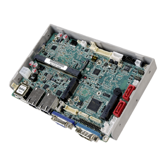
WAFER-CV-D25501/N26001 3.5" SBC 1.1 Introduction Figure 1-1: WAFER-CV-D25501/N26001 The WAFER-CV-D25501/N26001 3.5” motherboard is an Intel® Atom™ D2550/N2600 processor platform that supports one 1066 MHz or 800 MHz DDR3 SO-DIMM memory. The WAFER-CV-D25501/N26001 supports VGA display output and comes with two LVDS connectors supporting 24-bit or 18-bit LVDS screens. -
Page 17: Connectors
WAFER-CV-D25501/N26001 3.5" SBC 1.3 Connectors The connectors on the WAFER-CV-D25501/N26001 are shown in the figure below. Figure 1-2: Connectors Page 3... -
Page 18: Dimensions
WAFER-CV-D25501/N26001 3.5" SBC 1.4 Dimensions The main dimensions of the WAFER-CV-D25501/N26001 are shown in the diagram below. Page 4... -
Page 19: Figure 1-3: Wafer-Cv-D25501/N26001 Dimensions (Mm)
WAFER-CV-D25501/N26001 3.5" SBC Figure 1-3: WAFER-CV-D25501/N26001 Dimensions (mm) Page 5... -
Page 20: Data Flow
WAFER-CV-D25501/N26001 3.5" SBC 1.5 Data Flow F igure 1-4 shows the data flow between the system chipset, the CPU and other components installed on the motherboard. Figure 1-4: Data Flow Diagram Page 6... -
Page 21: Technical Specifications
WAFER-CV-D25501/N26001 3.5" SBC 1.6 Technical Specifications The WAFER-CV-D25501/N26001 technical specifications are listed below. Specification/Model WAFER-CV-D25501 WAFER-CV-N26001 3.5” Form Factor Intel® Atom™ D2550 1.86 GHz Intel® Atom™ N2600 1.6 GHz System CPU Intel® NM10 System Chipset One 1066 MHz DDR3/DDR3L (1.35V) One 800 MHz DDR3/DDR3L (1.35V) Memory SO-DIMM support (up to 4 GB) -
Page 22: Table 1-2: Wafer-Cv-D25501/N26001 Specifications
WAFER-CV-D25501/N26001 3.5" SBC Specification/Model WAFER-CV-D25501 WAFER-CV-N26001 One 3-pin CPU fan connector One 3-pin system fan connector Keyboard/mouse One internal pin-header connector SATA Two SATA 3Gb/s ports with 5V power Six USB 2.0/1.1 devices supported: Two by external connectors Four by on-board pin headers 12 V only Power Supply AT and ATX support... -
Page 23: Packing List
WAFER-CV-D25501/N26001 3.5" SBC Chapter Packing List Page 9... -
Page 24: Anti-Static Precautions
WAFER-CV-D25501/N26001 3.5" SBC 2.1 Anti-static Precautions WARNING! Static electricity can destroy certain electronics. Make sure to follow the ESD precautions to prevent damage to the product, and injury to the user. Make sure to adhere to the following guidelines: Wear an anti-static wristband: Wearing an anti-static wristband can prevent electrostatic discharge. -
Page 25: Packing List
WAFER-CV-D25501/N26001 3.5" SBC 2.3 Packing List NOTE: If any of the components listed in the checklist below are missing, do not proceed with the installation. Contact the IEI reseller or vendor the WAFER-CV-D25501/N26001 was purchased from or contact an IEI sales representative directly... -
Page 26: Optional Items
WAFER-CV-D25501/N26001 3.5" SBC Quantity Item and Part Number Image Mini jumper pack One Key Recovery CD Utility CD Quick Installation Guide Table 2-1: Packing List 2.4 Optional Items The following are optional components which may be separately purchased: Item and Part Number Image Dual USB cable (wo bracket) (P/N: 32001-008600-100-RS) -
Page 27: Connectors
WAFER-CV-D25501/N26001 3.5" SBC Chapter Connectors Page 13... -
Page 28: Peripheral Interface Connectors
WAFER-CV-D25501/N26001 3.5" SBC 3.1 Peripheral Interface Connectors This chapter details all the jumpers and connectors. 3.1.1 WAFER-CV-D25501/N26001 Layout The figure below shows all the connectors and jumpers. Figure 3-1: Connectors and Jumpers Page 14... -
Page 29: Peripheral Interface Connectors
WAFER-CV-D25501/N26001 3.5" SBC 3.1.2 Peripheral Interface Connectors The table below lists all the connectors on the board. Connector Type Label 5 V SATA power connectors 2-pin wafer SATA_PWR1, SATA_PWR2 12 V power connector 4-pin Molex power connector Audio connector 10-pin box header AUDIO1 Backlight inverter connectors 5-pin wafer... -
Page 30: External Interface Panel Connectors
WAFER-CV-D25501/N26001 3.5" SBC 3.1.3 External Interface Panel Connectors The table below lists the connectors on the external I/O panel. Connector Type Label Dual USB port Dual USB port USB1 Ethernet connectors RJ-45 LAN1, LAN2 RS-232 serial port connector Male DB-9 COM1 VGA connector 15-pin female... -
Page 31: Power Connector
WAFER-CV-D25501/N26001 3.5" SBC Pin No. Description Ground Table 3-3: 5 V SATA Power Connector Pinouts 3.2.2 12 V Power Connector CN Label: CN Type: 4-pin Molex power connector CN Location: See Figure 3-3 CN Pinouts: See Table 3-4 The ATX power connector connects to an ATX power supply. Figure 3-3: 12 V Power Connector Location Description +12V... -
Page 32: Backlight Inverter Connectors
WAFER-CV-D25501/N26001 3.5" SBC The 10-pin audio connector is connected to external audio devices including speakers and microphones for the input and output of audio signals to and from the system. Figure 3-4: Audio Connector Location Description Description Line-out_R Line-in_R AUD_GND AUD_GND Line-out _L Line-in _L... -
Page 33: Battery Connector
WAFER-CV-D25501/N26001 3.5" SBC Figure 3-5: Backlight Inverter Connector Locations Description LCD_BKLTCTL GROUND +12V GROUND LCD_BKLEN Table 3-6: Backlight Inverter Connector Pinouts 3.2.5 Battery Connector CAUTION: Risk of explosion if battery is replaced by an incorrect type. Only certified engineers should replace the on-board battery. Dispose of used batteries according to instructions and local regulations. -
Page 34: Digital Input/Output (Dio) Connector
WAFER-CV-D25501/N26001 3.5" SBC CN Location: See Figure 3-6 CN Pinouts: See Table 3-7 This is connected to the system battery. The battery provides power to the system clock to retain the time when power is turned off. Figure 3-6: Battery Connector Location Description Battery+ Table 3-7: Battery Connector Pinouts... -
Page 35: Fan Connectors
WAFER-CV-D25501/N26001 3.5" SBC Figure 3-7: Digital I/O Connector Location Description Description Output 3 Output 2 Output 1 Output 0 Input 3 Input 2 Input 1 Input 0 Table 3-8: Digital I/O Connector Pinouts 3.2.7 Fan Connectors CN Label: CPU_FAN1, SYS_FAN1 3-pin wafer CN Type: CN Location:... -
Page 36: Keyboard/Mouse Connector
WAFER-CV-D25501/N26001 3.5" SBC Figure 3-8: Fan Connector Locations PIN NO. DESCRIPTION +12 V Fan Speed Detect Table 3-9: Fan Connector Pinouts 3.2.8 Keyboard/Mouse Connector CN Label: KB_MS1 6-pin wafer CN Type: CN Location: See Figure 3-9 CN Pinouts: See Table 3-10 The keyboard and mouse connector can be connected to a standard PS/2 cable or PS/2 Y-cable to add keyboard and mouse functionality to the system. -
Page 37: Lvds1 Connector
WAFER-CV-D25501/N26001 3.5" SBC Figure 3-9: Keyboard/Mouse Connector Location Description +5 V KB DATA MS DATA MS CLK KB DATA KB CLK GROUND Table 3-10: Keyboard/Mouse Connector Pinouts 3.2.9 LVDS1 Connector CN Label: LVDS1 CN Type: 20-pin crimp CN Location: See Figure 3-10 See Table 3-11 CN Pinouts: The 20-pin LVDS LCD connector can be connected to an 18-bit/24-bit single-channel... -
Page 38: Lvds2 Connector
WAFER-CV-D25501/N26001 3.5" SBC Figure 3-10: LVDS1 Connector Location Description Description LVDS_DATA0 LVDS_DATA0# LVDS_DATA1 LVDS_DATA1# LVDS_DATA2 LVDS_DATA2# LVDS_CLK LVDS_CLK# LVDS_DATA3 LVDS_DATA3# LDDC_DATA LDDC_CLK VCC_LCD VCC_LCD VCC_LCD VCC_LCD Table 3-11: LVDS1 Connector Pinouts 3.2.10 LVDS2 Connector CN Label: LVDS2 CN Type: 30-pin crimp CN Location: See Figure 3-11 CN Pinouts:... -
Page 39: Figure 3-11: Lvds2 Connector Location
WAFER-CV-D25501/N26001 3.5" SBC Figure 3-11: LVDS2 Connector Location Description Description LVDS_DATA0 LVDS_DATA0# LVDS_DATA1 LVDS_DATA1# LVDS_DATA2 LVDS_DATA2# LVDS_CLK1 LVDS_CLK1# LVDS_DATA3 LVDS_DATA3# LVDS_DATA4 LVDS_DATA4# LVDS_DATA5 LVDS_DATA5# LVDS_DATA6 LVDS_DATA6# LVDS_CLK2 LVDS_CLK2# LVDS_DATA7 LVDS_DATA7# VCC_LCD VCC_LCD VCC_LCD VCC_LCD Table 3-12: LVDS2 Connector Pinouts Page 25... -
Page 40: Lvds2 Backlight Control Connector
WAFER-CV-D25501/N26001 3.5" SBC 3.2.11 LVDS2 Backlight Control Connector CN Label: 6-pin wafer CN Type: CN Location: See Figure 3-12 CN Pinouts: See Table 3-13 This connector allows control of the LVDS2 panel backlight. Figure 3-12: LVDS2 Backlight Control Connector Location Function Description PWRDN... -
Page 41: Figure 3-13: Pcie Mini Card Slot Locations
WAFER-CV-D25501/N26001 3.5" SBC NOTE: The M_PCIE2 slot supports mSATA devices. Figure 3-13: PCIe Mini Card Slot Locations Description Description PCIE_WAKE# VCC3 1.5V PCIE_CLK# PCIE_CLK PCIRST# PCIE_RXN VCC3 PCIE_RXP 1.5V SMBCLK PCIE_TXN SMBDATA PCIE_TXP USBD- Page 27... -
Page 42: Power & Hdd Led Connector
WAFER-CV-D25501/N26001 3.5" SBC Description Description USBD+ VCC3 VCC3 1.5V VCC3 Table 3-14: PCIe Mini Card Slot Pinouts 3.2.13 Power & HDD LED Connector CN Label: CN Type: 6-pin wafer CN Location: See Figure 3-14 CN Pinouts: See Table 3-15 The LED connector connects to an HDD indicator LED and a power LED on the system chassis to inform the user about HDD activity and the power on/off status of the system. -
Page 43: Power Button Connector
WAFER-CV-D25501/N26001 3.5" SBC Description Power LED+ Power LED- HDD LED+ HDD LED- Table 3-15: Power & HDD LED Connector Pinouts 3.2.14 Power Button Connector CN Label: PWR_BTN1 CN Type: 2-pin wafer CN Location: See Figure 3-15 CN Pinouts: See Table 3-16 The power button connector is connected to a power switch on the system chassis to enable users to turn the system on and off. -
Page 44: Reset Button Connector
WAFER-CV-D25501/N26001 3.5" SBC 3.2.15 Reset Button Connector CN Label: RST_BTN1 2-pin wafer CN Type: CN Location: See Figure 3-16 CN Pinouts: See Table 3-17 The reset button connector is connected to a reset switch on the system chassis to enable users to reboot the system when the system is turned on. -
Page 45: Rs-422/485 Serial Port Connector
WAFER-CV-D25501/N26001 3.5" SBC Figure 3-17: RS-232 Serial Port Connector Locations Description Description Table 3-18: RS-232 Serial Port Connector Pinouts 3.2.17 RS-422/485 Serial Port Connector CN Label: COM4 4-pin wafer CN Type: CN Location: See Figure 3-18 CN Pinouts: See Table 3-19 NOTE: These pins are shared with those on the main serial port. -
Page 46: Sata Drive Connectors
WAFER-CV-D25501/N26001 3.5" SBC Figure 3-18: RS-422/485 Connector Location Description Description RXD422- TXD422+/TXD485+ RXD422+ TXD422-/TXD485- Table 3-19: RS-422/485Connector Pinouts 3.2.18 SATA Drive Connectors CN Label: SATA1, SATA2 CN Type: 7-pin SATA drive connector See Figure 3-19 CN Location: CN Pinouts: See Table 3-20 The SATA drive connectors can be connected to SATA drives and support up to 3Gb/s data transfer rate. -
Page 47: Usb Connectors
WAFER-CV-D25501/N26001 3.5" SBC Description Table 3-20: SATA Drive Connector Pinouts 3.2.19 USB Connectors CN Label: USB2, USB3 CN Type: 8-pin header CN Location: See Figure 3-20 CN Pinouts: See Table 3-21 Each USB connector provides connectivity to two USB 1.1/2.0 ports. Figure 3-20: USB Connector Locations Description Description... -
Page 48: External Peripheral Interface Connector Panel
WAFER-CV-D25501/N26001 3.5" SBC Description Description USB_VCC Table 3-21: USB Connector Pinouts 3.3 External Peripheral Interface Connector Panel The figure below shows the external peripheral interface connector (EPIC) panel. The EPIC panel consists of the following: Figure 3-21: External Peripheral Interface Connector 3.3.1 Ethernet Connectors CN Label: LAN1, LAN2... -
Page 49: Serial Port Connector (Com1)
WAFER-CV-D25501/N26001 3.5" SBC Figure 3-22: RJ-45 Ethernet Connector Description Description on: linked off: 10 Mb/s blinking: data is being sent/received green: 100 Mb/s orange: 1000 Mb/s Table 3-23: RJ-45 Ethernet Connector LEDs 3.3.2 Serial Port Connector (COM1) CN Label: COM1 Male DB-9 connector CN Type: CN Location:... -
Page 50: Usb Connectors
WAFER-CV-D25501/N26001 3.5" SBC 3.3.3 USB Connectors CN Label: USB1 Dual USB port CN Type: CN Location: See Figure 3-21 CN Pinouts: See Table 3-25 The ports connect to both USB 2.0 and USB 1.1 devices. Description Description USB_VCC USB_VCC DATA- DATA- DATA+ DATA+... -
Page 51: Figure 3-24: Vga Connector
WAFER-CV-D25501/N26001 3.5" SBC Figure 3-24: VGA Connector NOTE: Due to Intel® GMA driver limitation, the monitor connected to the VGA connector may become extended desktop or not have signal to it after restarting from the graphics driver installation. To work out this limitation, press the Ctrl+Alt+F1 hotkey to switch the primary display to CRT mode. -
Page 52: Installation
WAFER-CV-D25501/N26001 3.5" SBC Chapter Installation Page 38... -
Page 53: Anti-Static Precautions
WAFER-CV-D25501/N26001 3.5" SBC 4.1 Anti-static Precautions WARNING: Failure to take ESD precautions during the installation of the WAFER-CV-D25501/N26001 may result in permanent damage to the WAFER-CV-D25501/N26001 and severe injury to the user. Electrostatic discharge (ESD) can cause serious damage to electronic components, including the WAFER-CV-D25501/N26001. - Page 54 WAFER-CV-D25501/N26001 3.5" SBC WARNING: The installation instructions described in this manual should be carefully followed in order to prevent damage to the components and injury to the user. Before and during the installation please DO the following: Read the user manual: The user manual provides a complete description of the WAFER-CV-D25501/N26001 installation instructions and configuration options.
-
Page 55: So-Dimm Installation
WAFER-CV-D25501/N26001 3.5" SBC 4.3 SO-DIMM Installation WARNING: Using incorrectly specified SO-DIMM may cause permanent damage to the WAFER-CV-D25501/N26001. Please make sure the purchased SO-DIMM complies with memory specifications WAFER-CV-D25501/N26001. SO-DIMM specifications compliant with the WAFER-CV-D25501/N26001 are listed in Chapter 1. To install a SO-DIMM into a SO-DIMM socket, please follow the steps below and refer to Figure 4-1. -
Page 56: Jumper Settings
WAFER-CV-D25501/N26001 3.5" SBC Step 5: Secure the SO-DIMM. Release the arms on the SO-DIMM socket. They clip into place and secure the SO-DIMM in the socket.Step 0: 4.4 Jumper Settings NOTE: A jumper is a metal bridge used to close an electrical circuit. -
Page 57: Clear Cmos Jumper
WAFER-CV-D25501/N26001 3.5" SBC The AT/ATX power selection jumper specifies the system power mode as AT or ATX. Setting Description Short 1-2 Use ATX power (Default) Use AT power Table 4-2: AT/ATX Power Selection Jumper Settings Figure 4-2: AT/ATX Power Selection Jumper Location 4.4.2 Clear CMOS Jumper Jumper Label: Jumper Type:... -
Page 58: Lvds1 Voltage Selection
WAFER-CV-D25501/N26001 3.5" SBC Figure 4-3: Clear CMOS Jumper Location 4.4.3 LVDS1 Voltage Selection WARNING: Permanent damage to the screen and WAFER-CV-D25501/N26001 may occur if the wrong voltage is selected with this jumper. Please refer to the user guide that came with the monitor to select the correct voltage. -
Page 59: Lvds2 Voltage Selection
WAFER-CV-D25501/N26001 3.5" SBC Figure 4-4: LVDS1 Voltage Selection Jumper Location 4.4.4 LVDS2 Voltage Selection WARNING: Permanent damage to the screen and WAFER-CV-D25501/N26001 may occur if the wrong voltage is selected with this jumper. Please refer to the user guide that came with the monitor to select the correct voltage. -
Page 60: Lvds2 Panel Type Selection Jumper
WAFER-CV-D25501/N26001 3.5" SBC Figure 4-5: LVDS2 Voltage Selection Jumper Location 4.4.5 LVDS2 Panel Type Selection Jumper Jumper Label: Jumper Type: 4-pin switch Jumper Settings: See Table 4-6 See Figure 4-6 Jumper Location: Sets the panel type of the LVDS2 video channel. Pin No. -
Page 61: Chassis Installation
WAFER-CV-D25501/N26001 3.5" SBC Pin No. EDID Resolution Color Depth Channel 4321 1100 1680 x 1050 @ 60Hz 24-bit Dual 1101 1600 x 1200 @ 60Hz 24-bit Dual 1110 1920 x 1080 @ 60Hz 24-bit Dual 1111 1920 x 1200 @ 60Hz 24-bit Dual Table 4-6: LVDS2 Panel Resolution... -
Page 62: Figure 4-7: Heat Sink Retention Screws
WAFER-CV-D25501/N26001 3.5" SBC WARNING: When running the WAFER-CV-D25501/N26001, do not put the WAFER-CV-D25501/N26001 directly on a surface that can not dissipate system heat, especially the wooden or plastic desk. It is highly recommended to run the WAFER-CV-D25501/N26001 on a heat dissipation surface or using copper pillars to hold the board up from the desk below When the WAFER-CV-D25501/N26001 is shipped it is secured to a heat sink with five retention screws. -
Page 63: Motherboard Installation
WAFER-CV-D25501/N26001 3.5" SBC 4.5.2 Motherboard Installation Each side of the heat sink enclosure has several screw holes allowing the WAFER-CV-D25501/N26001 to be mounted into a chassis (please refer to Figure 1-3 for the detailed dimensions). The user can design or select a chassis that has screw holes matching up with the holes on the heat sink enclosure for installing the WAFER-CV-D25501/N26001. -
Page 64: Internal Peripheral Device Connections
WAFER-CV-D25501/N26001 3.5" SBC 4.6 Internal Peripheral Device Connections This section outlines the installation of peripheral devices to the on-board connectors. 4.6.1 Audio Kit Installation The Audio Kit that came with the WAFER-CV-D25501/N26001 connects to the 10-pin audio connector on the WAFER-CV-D25501/N26001. The audio kit consists of three audio jacks. -
Page 65: Lvds Lcd Installation
WAFER-CV-D25501/N26001 3.5" SBC Step 3: Connect the audio devices. Connect one speaker to the line-in audio jack, one speaker to the line-out audio jack and a microphone to the mic-in audio jack. 4.6.2 LVDS LCD Installation The WAFER-CV-D25501/N26001 can be connected to a TFT LCD screen through the LVDS crimp connectors... -
Page 66: Figure 4-10: Lvds Connector
WAFER-CV-D25501/N26001 3.5" SBC Figure 4-10: LVDS Connector Step 3: Locate the backlight inverter connector. The locations of the backlight inverter connectors are shown in Chapter 3. Step 4: Connect backlight connector. Connect the backlight connector to the driver TFT LCD PCB as shown in Figure 4-11. When inserting the cable connector, make sure the pins are properly aligned. -
Page 67: Full-Size Pcie Mini Card Installation
WAFER-CV-D25501/N26001 3.5" SBC Figure 4-11: Backlight Inverter Connection 4.6.3 Full-size PCIe Mini Card Installation To install a full-size PCIe Mini card, please follow the steps below. Step 1: Locate the full-size PCIe Mini card slot. The location of the full-size PCIe Mini card slot is shown in Chapter 3. -
Page 68: Figure 4-12: Remove The Retention Screw For The Full-Size Pcie Mini Card
WAFER-CV-D25501/N26001 3.5" SBC Figure 4-12: Remove the Retention Screw for the Full-size PCIe Mini Card Step 3: Insert into the socket at an angle. Line up the notch on the card with the notch on the connector. Slide the PCIe Mini card into the socket at an angle of about 20º... -
Page 69: Half-Size Pcie Mini Card Installation
WAFER-CV-D25501/N26001 3.5" SBC Figure 4-14: Secure the Full-size PCIe Mini Card 4.6.4 Half-size PCIe Mini Card Installation To install a half-size PCIe Mini card, please follow the steps below. Step 1: Locate the half-size PCIe Mini card slot. The location of the half-size PCIe Mini card slot is shown in Chapter 3. -
Page 70: Sata Drive Connection
WAFER-CV-D25501/N26001 3.5" SBC Step 3: Insert into the socket at an angle. Line up the notch on the card with the notch on the connector. Slide the PCIe Mini card into the socket at an angle of about 20º (Figure 4-16). Figure 4-16: Insert the Half-size PCIe Mini Card into the Socket at an Angle Step 4: Secure the half-size PCIe Mini card. -
Page 71: Single Rs-232 Cable
WAFER-CV-D25501/N26001 3.5" SBC Step 1: Locate the SATA connector and the SATA power connector. The locations of the connectors are shown in Chapter 3. Step 2: Insert the cable connector. Insert the cable connector into the on-board SATA drive connector and the SATA power connector. See Figure 4-18. Figure 4-18: SATA Drive Cable Connection Step 3: Connect the cable to the SATA disk. -
Page 72: Keyboard/Mouse Y-Cable Connector
WAFER-CV-D25501/N26001 3.5" SBC Step 1: Locate the connector. The locations of the RS-232 connectors are shown in Chapter 3. Step 2: Insert the cable connector. Insert the connector into the serial port header. See Figure 4-19. A key on the front of the cable connector ensures the connector can only be installed in one direction. -
Page 73: Figure 4-20: Keyboard/Mouse Y-Cable Connection
WAFER-CV-D25501/N26001 3.5" SBC Step 1: Locate the connector. The location of the keyboard/mouse Y-cable connector is shown in Chapter 3. Step 2: Align the connectors. Correctly align pin 1 on the cable connector with pin 1 on the WAFER-CV-D25501/N26001 keyboard/mouse connector. See Figure 4-20. Step 3: Insert the cable connectors. - Page 74 WAFER-CV-D25501/N26001 3.5" SBC both marked. Please make sure the keyboard and mouse are connected to the correct PS/2 connector. Page 60...
-
Page 75: Bios
WAFER-CV-D25501/N26001 3.5" SBC Chapter BIOS Page 61... -
Page 76: Introduction
WAFER-CV-D25501/N26001 3.5" SBC 5.1 Introduction The BIOS is programmed onto the BIOS chip. The BIOS setup program allows changes to certain system settings. This chapter outlines the options that can be changed. NOTE: Some of the BIOS options may vary throughout the life cycle of the product and are subject to change without prior notice. -
Page 77: Getting Help
WAFER-CV-D25501/N26001 3.5" SBC Function Page Up key Move to the next page Page Dn key Move to the previous page Esc key Main Menu – Quit and not save changes into CMOS Status Page Setup Menu and Option Page Setup Menu -- Exit current page and return to Main Menu General help, only for Status Page Setup Menu and Option Page Setup Menu... -
Page 78: Main
WAFER-CV-D25501/N26001 3.5" SBC 5.2 Main The Main BIOS menu (BIOS Menu 1) appears when the BIOS Setup program is entered. The Main menu gives an overview of the basic system information. Aptio Setup Utility – Copyright (C) 2011 American Megatrends, Inc. Main Advanced Chipset... -
Page 79: Advanced
WAFER-CV-D25501/N26001 3.5" SBC System Time [xx:xx:xx] Use the System Time option to set the system time. Manually enter the hours, minutes and seconds. 5.3 Advanced Use the Advanced menu (BIOS Menu 2) to configure the CPU and peripheral devices through the following sub-menus: WARNING: Setting the wrong values in the sections below may cause the system to malfunction. -
Page 80: Rtc Wake Settings
WAFER-CV-D25501/N26001 3.5" SBC Aptio Setup Utility – Copyright (C) 2011 American Megatrends, Inc. Advanced ACPI Settings Select the highest ACPI sleep state the system will enter when the ACPI Sleep State [S1 (CPU Stop Clock)] SUSPEND button is pressed. ---------------------- : Select Screen ↑... -
Page 81: Bios Menu 4: Rtc Wake Settings
WAFER-CV-D25501/N26001 3.5" SBC Aptio Setup Utility – Copyright (C) 2011 American Megatrends, Inc. Advanced Wake system with Fixed Time [Disabled] Enable or disable System wake on alarm event. When enabled, System will wake on the date::hr::min::sec specified ---------------------- : Select Screen ↑... -
Page 82: Cpu Configuration
WAFER-CV-D25501/N26001 3.5" SBC 5.3.3 CPU Configuration Use the CPU Configuration menu (BIOS Menu 5) to view detailed CPU specifications and configure the CPU. Aptio Setup Utility – Copyright (C) 2011 American Megatrends, Inc. Advanced CPU Configuration Enabled for Windows XP and Linux (OS optimized Processor Type Intel(R) Atom(TM) -
Page 83: Ide Configuration
WAFER-CV-D25501/N26001 3.5" SBC Hyper-Threading [Enabled] Use the Hyper-Threading BIOS option to enable or disable the Intel Hyper-Threading Technology. Disabled Disables the Intel Hyper-Threading Technology. Enables the Intel Hyper-Threading Technology. Enabled EFAULT 5.3.4 IDE Configuration Use the IDE Configuration menu (BIOS Menu 6) to change and/or set the configuration of the SATA devices installed in the system. -
Page 84: Usb Configuration
WAFER-CV-D25501/N26001 3.5" SBC 5.3.5 USB Configuration Use the USB Configuration menu (BIOS Menu 7) to read USB configuration information and configure the USB settings. Aptio Setup Utility – Copyright (C) 2011 American Megatrends, Inc. Advanced USB Configuration Enables Legacy USB support. -
Page 85: F81866 Super Io Configuration
WAFER-CV-D25501/N26001 3.5" SBC 5.3.6 F81866 Super IO Configuration Use the F81866 Super IO Configuration menu (BIOS Menu 8) to set or change the configurations for the serial ports. Aptio Setup Utility – Copyright (C) 2011 American Megatrends, Inc. Advanced F81866 Super IO Configuration Set Parameters of Serial Port 1 (COMA) F81866 Super IO Chip... - Page 86 WAFER-CV-D25501/N26001 3.5" SBC 5.3.6.1.1 Serial Port 1 Configuration Serial Port [Enabled] Use the Serial Port option to enable or disable the serial port. Disabled Disable the serial port Enable the serial port Enabled EFAULT Change Settings [Auto] Use the Change Settings option to change the serial port IO port address and interrupt address.
- Page 87 WAFER-CV-D25501/N26001 3.5" SBC Change Settings [Auto] Use the Change Settings option to change the serial port IO port address and interrupt address. Auto The serial port IO port address and interrupt address EFAULT are automatically detected. Serial Port I/O port address is 2F8h and the interrupt IO=2F8h;...
- Page 88 WAFER-CV-D25501/N26001 3.5" SBC IO=3E8h; Serial Port I/O port address is 3E8h and the interrupt IRQ=10 address is IRQ10 Serial Port I/O port address is 3F8h and the interrupt IO=3F8h; address is IRQ10, 11 IRQ=10, 11 IO=2F8h; Serial Port I/O port address is 2F8h and the interrupt IRQ=10, 11 address is IRQ10, 11 IO=3E8h;...
-
Page 89: F81866 H/W Monitor
WAFER-CV-D25501/N26001 3.5" SBC IO=3F8h; Serial Port I/O port address is 3F8h and the interrupt IRQ=10, 11 address is IRQ10, 11 Serial Port I/O port address is 2F8h and the interrupt IO=2F8h; address is IRQ10, 11 IRQ=10, 11 IO=3E8h; Serial Port I/O port address is 3E8h and the interrupt IRQ=10, 11 address is IRQ10, 11 IO=2E8h;... -
Page 90: Smart Fan Mode Configuration
WAFER-CV-D25501/N26001 3.5" SBC PC Health Status The following system parameters and values are shown. The system parameters that are monitored are: System Temperatures: CPU Temperature System Temperature Fan Speeds: CPU Fan Speed System Fan Speed Voltages: +VCC_CPU +VCC_GFX +V1.05S +1.5_DDR3 VSB5V +V3.3S VSB3V... -
Page 91: Serial Port Console Redirection
WAFER-CV-D25501/N26001 3.5" SBC Aptio Setup Utility – Copyright (C) 2011 American Megatrends, Inc. Advanced Smart Fan Mode Configuration Smart Fan Mode Select CPU_FAN1 Smart Fan Control [Auto Duty-Cycle Mode] CPU Temperature 1 --------------------- CPU Temperature 2 : Select Screen ↑ ↓: Select Item CPU Temperature 3 CPU Temperature 4 Enter: Select... -
Page 92: Bios Menu 12: Serial Port Console Redirection
WAFER-CV-D25501/N26001 3.5" SBC Aptio Setup Utility – Copyright (C) 2011 American Megatrends, Inc. Advanced COM1 Console Redirection Console Redirection [Disabled] Enable or Disable > Console Redirection Settings COM2 Console Redirection [Disabled] --------------------- > Console Redirection Settings : Select Screen ↑ ↓: Select Item COM3 Enter: Select Console Redirection... - Page 93 WAFER-CV-D25501/N26001 3.5" SBC 9600 Sets the serial port transmission speed at 9600. Sets the serial port transmission speed at 19200. 19200 38400 Sets the serial port transmission speed at 38400. 57600 Sets the serial port transmission speed at 57600. 115200 Sets the serial port transmission speed at 115200.
-
Page 94: Iei Feature
WAFER-CV-D25501/N26001 3.5" SBC Sets the number of stop bits at 1. EFAULT Sets the number of stop bits at 2. 5.3.9 iEi Feature Use the iEi Feature menu (BIOS Menu 13) to configure One Key Recovery function. Aptio Setup Utility – Copyright (C) 2011 American Megatrends, Inc. Advanced iEi Feature Auto Recovery Function... -
Page 95: Chipset
WAFER-CV-D25501/N26001 3.5" SBC 5.4 Chipset Use the Chipset menu (BIOS Menu 14) to access the Host Bridge and Southbridge configuration menus. WARNING! Setting the wrong values for the Chipset BIOS selections in the Chipset BIOS menu may cause the system to malfunction. Aptio Setup Utility –... -
Page 96: Intel Igd Configuration
WAFER-CV-D25501/N26001 3.5" SBC Aptio Setup Utility – Copyright (C) 2011 American Megatrends, Inc. Chipset > Intel IGD Configuration Config Intel IGD Settings ******* Memory Information ******* Memory Frequency 1067 MHz(DDR3) Total Memory 1024 MB --------------------- DIMM#1 1024 MB : Select Screen ↑... - Page 97 WAFER-CV-D25501/N26001 3.5" SBC IGFX - Boot Type [VBIOS Default] Use the IGFX - Boot Type option to select the display device used by the system when it boots. Configuration options are listed below. VBIOS Default EFAULT LVDS1 LVDS2 LVDS1 Panel Type [800x600 LVDS] Use the LVDS1 Panel Type option to select the type of flat panel connected to the system.
-
Page 98: South Bridge Configuration
WAFER-CV-D25501/N26001 3.5" SBC 5.4.2 South Bridge Configuration Use the South Bridge Configuration menu (BIOS Menu 17) to configure the Southbridge chipset. Aptio Setup Utility – Copyright (C) 2011 American Megatrends, Inc. Chipset Auto Power Button Status [Disabled] Enable to reduce power consumption in system Power Saving Function(ERP) [Disabled]... -
Page 99: Boot
WAFER-CV-D25501/N26001 3.5" SBC 5.5 Boot Use the Boot menu (BIOS Menu 18) to configure system boot options. Aptio Setup Utility – Copyright (C) 2011 American Megatrends, Inc. Main Advanced Chipset Boot Security Save & Exit Boot Configuration Select the keyboard Bootup NumLock State [On] NumLock state... - Page 100 WAFER-CV-D25501/N26001 3.5" SBC Quiet Boot [Enabled] Use the Quiet Boot BIOS option to select the screen display when the system boots. Normal POST messages displayed Disabled Enabled OEM Logo displayed instead of POST messages EFAULT Launch PXE OpROM [Disabled] Use the Launch PXE OpROM option to enable or disable boot option for legacy network devices.
-
Page 101: Security
WAFER-CV-D25501/N26001 3.5" SBC 5.6 Security Use the Security menu (BIOS Menu 19) to set system and user passwords. Aptio Setup Utility – Copyright (C) 2011 American Megatrends, Inc. Main Advanced Chipset Boot Security Save & Exit Password Description Set Setup Administrator Password If ONLY the Administrator’s password is set, then this only limits access to Setup and is... -
Page 102: Bios Menu 20:Exit
WAFER-CV-D25501/N26001 3.5" SBC Aptio Setup Utility – Copyright (C) 2011 American Megatrends, Inc. Main Advanced Chipset Boot Security Save & Exit Save Changes and Reset Reset the system after Discard Changes and Reset saving the changes. Restore Defaults Save as User Defaults Restore User Defaults --------------------- : Select Screen... -
Page 103: Software Drivers
WAFER-CV-D25501/N26001 3.5" SBC Chapter Software Drivers Page 89... -
Page 104: Available Software Drivers
WAFER-CV-D25501/N26001 3.5" SBC 6.1 Available Software Drivers NOTE: The content of the CD may vary throughout the life cycle of the product and is subject to change without prior notice. Visit the IEI website or contact technical support for the latest updates. The following drivers can be installed on the system: Chipset Graphics... -
Page 105: Chipset Driver Installation
WAFER-CV-D25501/N26001 3.5" SBC 6.3 Chipset Driver Installation To install the chipset driver, please do the following. Step 1: Access the driver list. (See Section 6.2) Step 2: Click “1-Chipset”. Step 3: Go to the 32-bit or 64-bit folder that corresponds to your OS version. Step 4: Open the Intel Chipset Software Installation Utility folder. -
Page 106: Figure 6-2: Chipset Driver Welcome Screen
WAFER-CV-D25501/N26001 3.5" SBC Figure 6-2: Chipset Driver Welcome Screen Step 8: Click Next to continue. Step 9: The license agreement in Figure 6-3 appears. Step 10: Read the License Agreement. Step 11: Click Yes to continue. Page 92... -
Page 107: Figure 6-3: Chipset Driver License Agreement
WAFER-CV-D25501/N26001 3.5" SBC Figure 6-3: Chipset Driver License Agreement Step 12: The Read Me file in Figure 6-4 appears. Step 13: Click Next to continue. Figure 6-4: Chipset Driver Read Me File Page 93... -
Page 108: Figure 6-5: Chipset Driver Setup Operations
WAFER-CV-D25501/N26001 3.5" SBC Step 14: Setup Operations are performed as shown in Figure 6-5. Figure 6-5: Chipset Driver Setup Operations Step 15: Once the Setup Operations are complete, click Next to continue. Step 16: The Finish screen appears. Step 17: Select “Yes, I want to restart the computer now”... -
Page 109: Graphics Driver Installation
WAFER-CV-D25501/N26001 3.5" SBC Figure 6-6: Chipset Driver Installation Finish Screen 6.4 Graphics Driver Installation NOTE: Due to Intel® GMA driver limitation, the monitor connected to the VGA connector may become extended desktop or not have signal to it after restarting from the graphics driver installation. To work out this limitation, press the Ctrl+Alt+F1 hotkey to switch the primary display to CRT mode. -
Page 110: Figure 6-7: Graphics Driver Welcome Screen
WAFER-CV-D25501/N26001 3.5" SBC Step 5: The Welcome Screen in Figure 6-7 appears. Figure 6-7: Graphics Driver Welcome Screen Step 6: Click Next to continue. Step 7: The license agreement in Figure 6-8 appears. Step 8: Read the License Agreement. Step 9: Click Yes to continue. -
Page 111: Figure 6-8: Graphics Driver License Agreement
WAFER-CV-D25501/N26001 3.5" SBC Figure 6-8: Graphics Driver License Agreement Step 10: The Read Me file in Figure 6-9 appears. Step 11: Click Next to continue. Figure 6-9: Graphics Driver Read Me File Step 12: Setup Operations are performed as shown in Figure 6-10. Page 97... -
Page 112: Figure 6-10: Graphics Driver Setup Operations
WAFER-CV-D25501/N26001 3.5" SBC Figure 6-10: Graphics Driver Setup Operations Step 13: Once the Setup Operations are complete, click the Next icon to continue. Step 14: The Finish screen appears. Step 15: Select “Yes, I want to restart the computer now” and click the Finish icon. See Figure 6-11. -
Page 113: Lan Driver Installation
WAFER-CV-D25501/N26001 3.5" SBC 6.5 LAN Driver Installation To install the LAN driver, please do the following. Step 1: Access the driver list. (See Section 6.2) Step 2: Click “3-LAN”. Step 3: Go to the Win7 > Install_Win7_7048_09162011 folder. Step 4: Double click the setup icon. -
Page 114: Figure 6-13: Lan Driver Installation
WAFER-CV-D25501/N26001 3.5" SBC Figure 6-13: LAN Driver Installation Step 9: The program begins to install. Step 10: When the driver installation is complete, the screen in Figure 6-14 appears. Step 11: Click Finish to exit. Figure 6-14: LAN Driver Installation Complete Page 100... -
Page 115: Audio Driver Installation
WAFER-CV-D25501/N26001 3.5" SBC 6.6 Audio Driver Installation To install the Audio driver, please do the following. Step 1: Access the driver list. (See Section 6.2) Step 2: Click “4-Audio”. Step 3: Open the Win7 folder. Step 4: Double click the Vista_Win7_R263 icon. Step 5: The installation files are extracted as shown in Figure 6-15. -
Page 116: Figure 6-16: Audio Driver Welcome Screen
WAFER-CV-D25501/N26001 3.5" SBC Figure 6-16: Audio Driver Welcome Screen Step 7: Click Next to continue. Step 8: The program begins to install. Step 9: The installation progress can be monitored in the progress bar shown in Figure 6-17. Figure 6-17: Audio Driver Installation Step 10: When the driver installation is complete, the screen in Figure 6-18 appears. - Page 117 WAFER-CV-D25501/N26001 3.5" SBC Figure 6-18: Audio Driver Installation Complete Step 11: Select “Yes, I want to restart my computer now” and click Finish. Step 12: The system reboots. Page 103...
-
Page 118: A Regulatory Compliance
WAFER-CV-D25501/N26001 3.5" SBC Appendix Regulatory Compliance Page 104... - Page 119 WAFER-CV-D25501/N26001 3.5" SBC DECLARATION OF CONFORMITY This equipment has been tested and found to comply with specifications for CE marking. If the user modifies and/or installs other devices in the equipment, the CE conformity declaration may no longer apply. FCC WARNING This equipment complies with Part 15 of the FCC Rules.
-
Page 120: Bbios Options
WAFER-CV-D25501/N26001 3.5" SBC Appendix BIOS Options Page 106... - Page 121 WAFER-CV-D25501/N26001 3.5" SBC Below is a list of BIOS configuration options in the BIOS chapter. System Overview .........................64 System Date [xx/xx/xx] ......................64 System Time [xx:xx:xx] .......................65 ACPI Sleep State [S1 (CPU Stop Clock)] ................66 Wake system with Fixed Time [Disabled]................67 ...
- Page 122 WAFER-CV-D25501/N26001 3.5" SBC Quiet Boot [Enabled] ......................86 Launch PXE OpROM [Disabled] ..................86 Option ROM Messages [Force BIOS].................86 UEFI Boot [Disabled] ......................86 Administrator Password .....................87 User Password ........................87 Save Changes and Reset ....................88 Discard Changes and Reset ....................88 ...
-
Page 123: C Terminology
WAFER-CV-D25501/N26001 3.5" SBC Appendix Terminology Page 109... - Page 124 WAFER-CV-D25501/N26001 3.5" SBC AC ’97 Audio Codec 97 (AC’97) refers to a codec standard developed by Intel® in 1997. ACPI Advanced Configuration and Power Interface (ACPI) is an OS-directed configuration, power management, and thermal management interface. AHCI Advanced Host Controller Interface (AHCI) is a SATA Host controller register-level interface.
- Page 125 WAFER-CV-D25501/N26001 3.5" SBC DIMM Dual Inline Memory Modules are a type of RAM that offer a 64-bit data bus and have separate electrical contacts on each side of the module. The digital inputs and digital outputs are general control signals that control the on/off circuit of external devices or TTL devices.
- Page 126 WAFER-CV-D25501/N26001 3.5" SBC LVDS Low-voltage differential signaling (LVDS) is a dual-wire, high-speed differential electrical signaling system commonly used to connect LCD displays to a computer. POST The Power-on Self Test (POST) is the pre-boot actions the system performs when the system is turned-on. Random Access Memory (RAM) is volatile memory that loses data when power is lost.
-
Page 127: D Digital I/O Interface
WAFER-CV-D25501/N26001 3.5" SBC Appendix Digital I/O Interface Page 113... -
Page 128: Introduction
WAFER-CV-D25501/N26001 3.5" SBC D.1 Introduction The DIO connector on the WAFER-CV-D25501/N26001 is interfaced to GPIO ports on the Super I/O chipset. The digital inputs and digital outputs are generally control signals that control the on/off circuit of external devices or TTL devices. Data can be read or written to the selected address to enable the DIO functions. -
Page 129: Assembly Language Sample 1
WAFER-CV-D25501/N26001 3.5" SBC D.2 Assembly Language Sample 1 AX, 6F08H ;setting the digital port as input AL low byte = value AH – 6FH Sub-function: AL – 9 :Set the digital port as OUTPUT :Digital I/O input value D.3 Assembly Language Sample 2 AX, 6F09H ;setting the digital port as output BL, 09H... -
Page 130: E Watchdog Timer
WAFER-CV-D25501/N26001 3.5" SBC Appendix Watchdog Timer Page 116... - Page 131 WAFER-CV-D25501/N26001 3.5" SBC NOTE: The following discussion applies to DOS environment. Contact IEI support or visit the IEI website for specific drivers for other operating systems. The Watchdog Timer is provided to ensure that standalone systems can always recover from catastrophic conditions that cause the CPU to crash. This condition may have occurred by external EMIs or a software bug.
- Page 132 WAFER-CV-D25501/N26001 3.5" SBC NOTE: When exiting a program it is necessary to disable the Watchdog Timer, otherwise the system resets. EXAMPLE PROGRAM: ; INITIAL TIMER PERIOD COUNTER W_LOOP: AX, 6F02H ;setting the time-out value BL, 30 ;time-out value is 48 seconds ;...
-
Page 133: F Hazardous Materials Disclosure
WAFER-CV-D25501/N26001 3.5" SBC Appendix Hazardous Materials Disclosure Page 119... - Page 134 WAFER-CV-D25501/N26001 3.5" SBC The details provided in this appendix are to ensure that the product is compliant with the Peoples Republic of China (China) RoHS standards. The table below acknowledges the presences of small quantities of certain materials in the product, and is applicable to China RoHS only.
- Page 135 WAFER-CV-D25501/N26001 3.5" SBC 此附件旨在确保本产品符合中国 RoHS 标准。以下表格标示此产品中某有毒物质的含量符 合中国 RoHS 标准规定的限量要求。 本产品上会附有”环境友好使用期限”的标签,此期限是估算这些物质”不会有泄漏或突变”的 年限。本产品可能包含有较短的环境友好使用期限的可替换元件,像是电池或灯管,这些元 件将会单独标示出来。 部件名称 有毒有害物质或元素 铅 汞 镉 六价铬 多溴联苯 多溴二苯 醚 (Pb) (Hg) (Cd) (CR(VI)) (PBB) (PBDE) 壳体 显示 印刷电路板 金属螺帽 电缆组装 风扇组装 电力供应组装 电池 O: 表示该有毒有害物质在该部件所有物质材料中的含量均在 SJ/T11363-2006 (现由 GB/T 26572-2011 取代) 标准规定的限量要求以下。...
Need help?
Do you have a question about the WAFER-CV-D25501 Series and is the answer not in the manual?
Questions and answers